

Results 10,011 to 10,020 of 12091
Thread: Anandtech News
-
10-31-19, 01:51 PM #10011
Anandtech: Samsung Develops Intel Lakefield-Based Galaxy Book S: Always-Connected x86
Among several items at its developers conference this week, Samsung revealed that it was working on a version of its always-connected Galaxy Book S laptop powered by Intel’s Lakefield processor. When it becomes available in 2020, the notebook is expected to be the first mobile PC powered by Intel’s hybrid SoC, which containing a mix of high-performance and energy-efficient cores.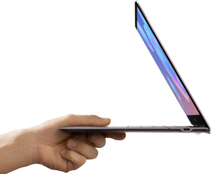
There are many laptop users nowadays who want their PCs to be very sleek, offer decent performance, be always connected to the Internet, and to last for a long time on a charge. Modern premium x86-based notebooks are very compact and can be equipped with a 4G/LTE modem, but even configured properly, the extra radio brings a hit to battery life over a non-modem model. The immediate solution is of course to use Intel’s low-power/energy-efficient Atom SoCs or Qualcomm's Snapdragon processors tailored for notebooks, but this will have an impact on performance.
To offer both performance and energy efficiency for always-connected notebooks, Intel has developed its Lakefield SoC that features one high-performance Ice Lake core, four energy-efficient Tremont cores, as well as Gen 11 graphics & media cores. Internally, Intel’s Lakefield consists of two dies — a 10 nm Compute die and a 14 nm Base die — integrated into one chip using the company’s Foveros 3D packaging technology to minimize its footprint. Courtesy of Foveros, the chip measures 12×12 mm and can be integrated into a variety of emerging always-connected devices.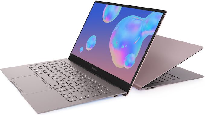
As it turns out, Samsung’s upcoming version of the 13.3-inch Galaxy Book S will be the first to use Intel’s Lakefield, where it will be paired with Intel’s 4G/LTE modem to offer Internet connectivity everywhere.
Samsung is not disclosing pricing or availability details for its Lakefield-powered Galaxy Book S; but since Intel plans to start production of the SoC this quarter, expect the machine to launch in 2020.
Related Reading:
- Samsung Announces Always-Connected Galaxy Book S Laptop with Snapdragon 8cx
- Samsung Unveils Galaxy Book2: 12-Inch, Snapdragon 850 with X20 LTE, 20 Hrs
- Hands-On with Industry’s First 5G Laptop: A Lenovo with Qualcomm’s 8cx SoC and X55 Modem
- Qualcomm Tech Summit, Day 3: Snapdragon 8cx, the New ACPC SoC
- Spotted: Qualcomm Snapdragon 8cx Wafer on 7nm
- Lenovo Announces Yoga C630: The First Windows on Snapdragon 850
- Huawei Readies Windows 10 Laptop Based on Qualcomm Snapdragon 850
Source: Intel/Samsung
More...
-
10-31-19, 04:20 PM #10012
Anandtech: Western Digital Launches WD Red SA500 Caching SSDs for NAS
Western Digital has introduced its new WD Red SA500 family of specialized SSDs, which are designed for caching data in NAS devices. The drives are available in four different capacities from 500 GB to 4 TB to satisfy demands of different customers. To maximize their compatibility, the SSDs feature a SATA 6 Gbps interface and come in M.2-2280 or 2.5-inch/7-mm form-factors.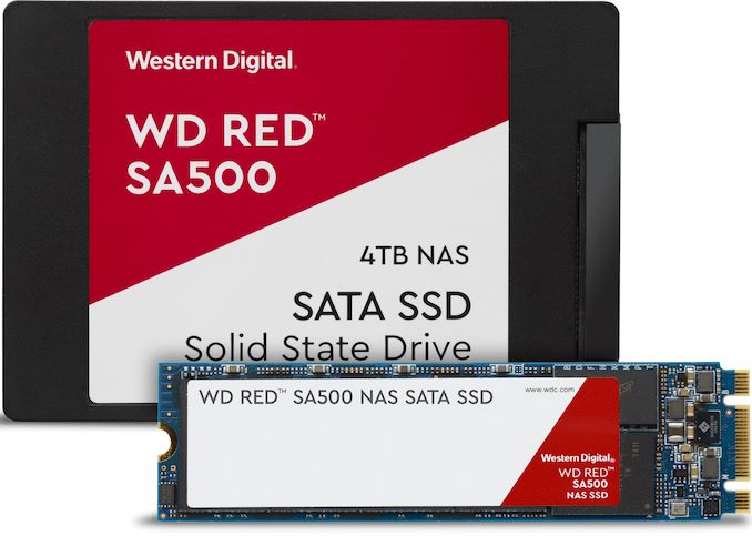
Now that many desktop PCs have either been replaced by laptops or are so small that they cannot house a decent number of capacious hard drives, NAS use is gaining traction among those individuals and small businesses who need to store fairly large amounts of data. To provide such customers high performance (which is comparable to that of internal storage), many NAS these days feature a 10GbE network adapter as well as a special bay (or bays) for a caching SSD. However, the vast majority of client SSDs on the market were not designed for pure caching workloads, which are more write-heavy than typical consumer workloads. Seagate with its IronWolf 110 was the first company to launch an SSD architected for NAS caching early this year and now Western Digital follows the suit with its WD Red SA500 family, which is broader than that offered by its rival.
While it's not being disclosed by the company, Western Digital’s WD Red SA500 SSDs are based on Marvell's proven 88SS1074 controller, and paired with the company’s 3D TLC NAND memory. When it comes to capacities, the new WD Red SA500 drives are available in two form-factors: M.2-2280 models offer 500 GB, 1 TB, and 2 TB capacities, whereas 2.5-inch/7-mm SKUs can store 500 GB, 1 TB, 2 TB and 4 TB of data.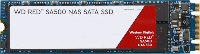
Performance-wise, the WD Red SA500 offers up to 560 MB/s sequential read speeds, up to 530 MB/s sequential write speeds, and up to 95K/85K random read/write IOPS, which is in line with advanced client SATA SSDs. But the key difference between typical client drives equipped with the same controller and the WD Red SA500 is a special firmware optimized for more evenly mixed workloads and engineered to ensure longevity. By contrast, client SSDs are tailored mostly for fast reads.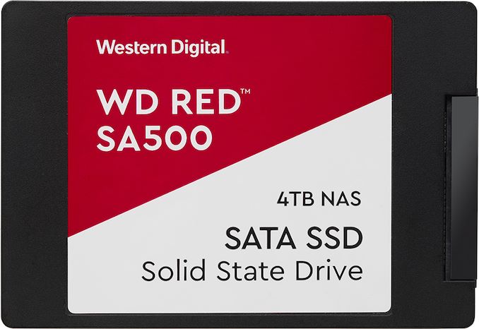
As far as endurance is concerned, the WD Red SA500 SSDs are rated for 0.32 – 0.38 DWPD over a five-year warranty period, which is in line with that of modern desktop drives. This is admittedly not especially high for a drive that can fill itself in under an hour, but presumably Western Digital confident that the caching algorithms in modern NASes are not so aggressive that the drives will be extensively rewritten. Moreover, at the end of the day we are talking about consumer as well as SMB-class NASes, where the expected workloads are lower than with enterprise systems.
Western Digital’s WD Red SA500 SSDs are currently available directly from the company, with broader availability expected in November. The cheapest 500 GB model costs $72 – $75 depending on the form-factor, the top-of-the-range M.2 2 TB SKU is priced at $297, whereas the highest-capacity 4 TB 2.5-inch model carries a $600 price tag.The WD Red SA500 Caching SSDs for NAS Capacity 500 GB 1 TB 2 TB 4 TB Model Number ? ? ? ? Controller Marvell 88SS1074 NAND Flash 3D TLC NAND Form-Factor, Interface M.2 M.2-2280, SATA 6 Gbps - DFF 2.5-inch/7-mm, SATA 6 Gbps Sequential Read 560 MB/s Sequential Write 530 MB/s Random Read IOPS 95K Random Write IOPS 85K 82K Pseudo-SLC Caching ? DRAM Buffer Yes, capacity unknown TCG Opal Encryption ? Power Consumption Avg Active 52 mW 60 mW 60 mW Max. Read 2050 mW 2550 mW 3000 mW Max. Write 3350 mW 3750 mW 3800 mW Slumber 56 mW 56 mW DEVSLP 5-7 mW 5-12 mW Warranty 5 years MTBF 2 million hours TBW 350 600 1300 2500 DWPD 0.38 0.32 0.35 0.34 UBER 1E10^17 Additional Information Link MSRP M.2 $72 ? $297 - DFF $75 ? ? $600
Related Reading: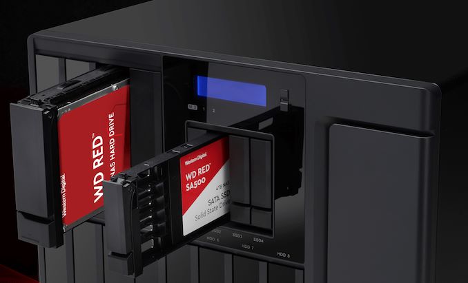
- Seagate Introduces IronWolf SSD for NAS
- QNAP Launches Mustang-200 Compute Accelerator for Network Attached Storage
- WD Adds Helium-Filled 10 TB NAS HDDs to WD Red, WD Red Pro Lineups
- Western Digital Introduces Its First Helium-Filled HDDs for Consumer Applications
Source: Western Digital
More...
-
11-01-19, 09:59 AM #10013
Anandtech: Sony to Build New Fab to Boost CMOS Sensor Output
Sony this week has revealed that the company will be building a new semiconductor fab to boost output of its CMOS sensors, as part of a broader effort to respond to growing demand for these products. The company will build the new fab at its Nagasaki Technology Center and expects it to tangibly increase their production of CMOS wafers.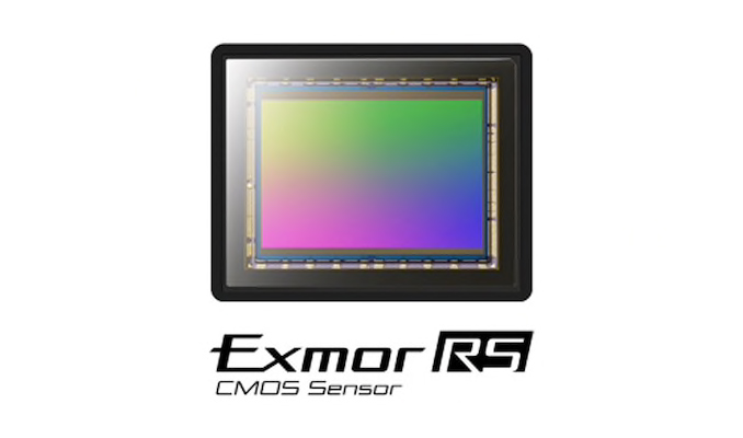
Being one of the leading suppliers of CMOS camera sensors for smartphones, Sony earns billions of dollars selling them. In the third quarter (Q2 FY2019) Sony’s Imaging and Sensing Solutions (I&SS) division earned $2.871 billion in revenue (up 56.3% year-over-year) and $706 million in profits*. As of late March 2018, Sony’s CMOS production capacity was 100 thousand 300-mm wafer starts per month, and the company is gradually increasing its output by improving efficiency of its fab space utilization and outsourcing part of the production. But that may not be enough.
In the coming years demand for CMOS sensors is going to grow because of several factors: smartphones now use not two (for main and selfie cameras), but three or even more camera modules; smartphone sensors are getting larger; and more devices are going to get computer vision support, requiring more sensors there as well.
In order to satisfy demand for such products, the company constantly improves its fabs and expects to boost their total output capacity to around 138 thousand of wafer starts per month by late March 2021. Furthermore, Sony plans to invest billions of dollars (PDF, page 152) in fab upgrades as well as building an additional fab (or even fabs) at its Nagasaki Technology Center. The new manufacturing facility (or facilities) is expected to start production sometime during the company's 2021 fiscal year, which starts on April 1, 2021. That being said, it is reasonable to expect that Sony is aiming to start construction of the facility in the coming months.
It is noteworthy that Sony’s semiconductor division (which is now called I&SS) reportedly has not invested anything in brand-new production facilities for 12 years. The company did acquire a semiconductor fab from Toshiba and then re-purposed it to make sensors in 2016, but this was not a new fab. Apparently, Sony now forecasts such high demand for sensors in the coming years that it has decided to invest in all-new production lines.
Sony’s statement reads as follows:
“We expect demand for our image sensors to continue to increase from next fiscal year as well due to the adoption of multi-sensor cameras and larger- sized sensors by smartphone makers.*For the sake of clarity, it is necessary to note that Sony’s I&SS division still produces some chips for Sony’s needs, so not 100% of its revenue comes from image sensors
In order to respond to this strong demand, we have further improved the efficiency of space utilization in our existing factories and have raised our production capacity target for the end of March 2021 from 130,000 wafers per month to 138,000 wafers per month.
Moreover, we have decided to move forward in stages with the investment we had been considering to build new fabs at our Nagasaki facility to accommodate demand from the fiscal year beginning April 1, 2021.
Through this action, we are working to continue growing the I&SS business so as to achieve the mid-range targets we established at the IR Day this year: 60% revenue share of the image sensor market and 20-25% ROIC in the fiscal year ending March 31, 2026.”
Related Reading:
- The Sony Xperia 1 Review: A 21:9 Take of the World
- Sony Xperia 1, the Long 21:9 Smartphone, Available for Pre-Order
- Samsung Unveils ISOCELL Bright HMX 108 MP Sensor for Smartphones
- Samsung Unveils 64 MP & 48 MP ISOCELL Bright Image Sensors for Smartphones
Sources: Sony, Sony, Nikkei, ElectronicsWeekly, Reuters
More...
-
11-01-19, 01:07 PM #10014
Anandtech: Western Digital Begins Shipments of 96-Layer 3D QLC-Based SSDs, Retail Pro
Western Digital announced this week that it has started shipments of its first products based on 3D QLC NAND memory. The initial devices to use the highly-dense flash memory are retail products (e.g., memory cards, USB flash drives, etc.) as well as external SSDs. Eventually, high-density 3D QLC NAND devices will be used to build high-capacity SSDs that will compete against nearline hard drives.
During Western Digital's quarterly earnings conference call earlier this week, Mike Cardano, president and COO of the company, said that in the third quarter of calendar 2019 (Q1 FY2020) the manufacturer “began shipping 96-layer 3D QLC-based retail products and external SSDs.” The executive did not elaborate which product lines now use 3D QLC NAND, though typically we see higher capacity NAND first introduced in products such as high-capacity memory cards and external drives.
Western Digital and its partner Toshiba Memory (now called Kioxia) were among the first companies to develop 64-layer 768 Gb 3D QLC NAND back in mid-2017 and even started sampling of these devices back then, but WD/Toshiba opted not to mass produce the NAND. Meanwhile, in mid-2018, Western Digital introduced its 96-layer 1.33 Tb 3D QLC NAND devices that could either enable to build storage products with considerably higher capacities, or cut costs of drives when compared to 3D TLC-based solutions.
At present, Western Digital’s 1.33 Tb 3D QLC NAND devices are the industry’s highest-capacity commercial NAND chips, so from this standpoint the company is ahead of its rivals. But while it makes a great sense to use 1.33 Tb 3D QLC NAND for advanced consumer storage devices, these memory chips were developed primarily for ultra-high-capacity SSDs that could rival nearline HDDs for certain applications.
It is hard to say when Western Digital commercializes such drives as the company is only starting to qualify 96-layer 3D QLC NAND for SSDs, but it will definitely be interesting to see which capacity points will be hit with the said memory.
On a related note, Western Digital also said that in Q3 2019 (Q1 FY2020), bit production of 96-layer 3D NAND exceeded bit production of 64-layer 3D NAND.
Related Reading:
- Western Digital Begins to Sample QLC BiCS4: 1.33 Tbit 96-Layer 3D NAND
- Western Digital Starts Shipments of Client SSDs Based on 96-Layer BICS4 3D NAND
- Western Digital Announces Four Bit Per Cell 64-Layer 3D NAND Flash
- Toshiba's 768Gb 3D QLC NAND Flash Memory: Matching TLC at 1000 P/E Cycles?
- Intel Announces SSD 665p: Denser, Faster QLC NAND
- Micron: Shipments of 3D QLC for SSDs Nearly Double QoQ as Wafer Starts Cut Again
Source: Western Digital
More...
-
11-01-19, 01:07 PM #10015
Anandtech: Rambus Demonstrates GDDR6 Running At 18 Gbps
While GDDR6 is currently available at speeds up to 14Gbps, and 16Gbps speeds are right around the corner, if the standard is going to have as long a lifespan as GDDR5, then it can't stop there. To that end, Rambus this week demonstrated operation of its GDDR6 memory subsystem at a data transfer rate of 18 GigaTransfers/second, a new record for the company. Rambus’s controller and PHY can deliver a peak bandwidth of 72 GB/s from a single 32-bit GDDR6 DRAM chip, or a whopping 576 GB/s from a 256-bit memory subsystem, which is what we're commonly seeing on graphics cards today.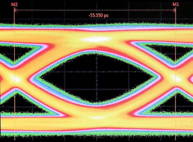
The Rambus demonstration involved the company’s silicon-proven GDDR6 PHY implemented using one of TSMC’s 7 nm process nodes, accompanied by Northwest Logic’s GDDR6 memory controller and GDDR6 chips from an unknown maker. According to a transmit eye screenshot published by Rambus, the subsystem worked fine and the signals were clean.
Both GDDR6 controller and PHY can be licensed from Rambus by developers of SoCs, so the demonstration is both a testament to how well the company’s highly-integrated 7 nm GDDR6 solution works, and a means to promote their IP offerings.
It is noteworthy that Rambus, along with Micron and a number of other companies, has been encouraging the use of GDDR6 memory in products besides GPUs for quite some time. Various accelerators for AI, ML, and HPC workloads as well as networking gear and autonomous driving systems greatly benefit from the technology's high memory bandwidth and are therefore a natural fit for GDDR6. The demonstration is meant to show companies developing SoCs that Rambus has a fine GDDR6 memory solution implemented using a leading-edge process technology that can be easily integrated (with the help of engineers from Rambus) into their designs.
For the graphics crowd, Rambus’ demonstration gives a hint of what to expect from upcoming implementations of GDDR6 memory subsystems and indicates that GDDR6 still has some additional room for growth in terms of data transfer rates.
Related Reading:
- Micron, Rambus, & Others Team Up To Spur GDDR6 Adoption in Non-GPU Products
- Cadence Tapes Out GDDR6 IP on Samsung 7LPP Using EUV
- Samsung Updates on GDDR6 Portfolio: 8 Gb and 16 Gb at Multiple Speeds
- Samsung Pre-Announces 16 Gbps GDDR6 Chips for Next-Gen Graphics Cards
Source: Rambus
More...
-
11-01-19, 05:57 PM #10016
Anandtech: LGs E9, C9 & B9 OLED TVs to Get NVIDIA G-Sync via Firmware Update
Back in September, LG and NVIDIA teamed up to enable G-Sync variable refresh rate support on select OLED televisions. Starting this week and before the end of the year LG will issue firmware updates that add support for the capability on the company’s latest premium OLED TVs.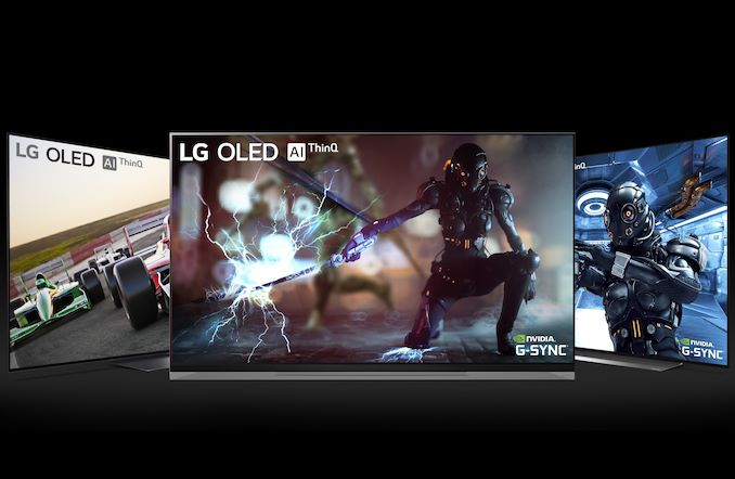
LG's 2019 OLED TVs have been making waves throughout the gaming community since their launch earlier this year. The TVs are among the first to support HDMI 2.1's standardized variable refresh rate technology, adding a highly demanded gaming feature to LG's already popular lineup of TVs. This has put LG's latest generation of TVs on the cutting edge, and, along with Microsoft's Xbox One X (the only HDMI-VRR source device up until now), the duo of devices has been serving as a pathfinder for HDMI-VRR in general.
Now, NVIDIA is getting into the game by enabling support for HDMI-VRR on recent video cards, as well as working with LG to get the TVs rolled into the company's G-Sync Compatible program. The two companies have begun rolling out the final pieces needed for variable refresh support this week, with LG releasing a firmware update for their televisions, while NVIDIA has started shipping a new driver with support for the LG TVs.
On the television side of matters, LG and NVIDIA have added support for the 2019 E9 (65 and 55 inches), C9 (77, 65 and 55 inches), and B9 (65 and 55 inches) families of TVs, all of which have been shipping with variable refresh support for some time now.
The more interesting piece of the puzzle is arguably on the video card side of matters, where NVIDIA is enabling support for the TVs on their Turing generation of video cards, which covers the GeForce RTX 20 series as well as the GeForce GTX 16 series of cards. At a high level, NVIDIA and LG are branding this project as adding G-Sync Compatible support for the new TVs. But, as NVIDIA has confirmed, under the hood this is all built on top of HDMI-VRR functionality. Meaning that as of this week, NVIDIA has just added support for HDMI's variable refresh standard to their Turing video cards.
While HDMI-VRR was introduced as part of HDMI 2.1, the feature is an optional extension to HDMI and is not contingent on the latest standard's bandwidth upgrades. This has allowed manufacturers to add support for the tech to HDMI 2.0 devices, which is exactly what has happened with the Xbox One X and now NVIDIA's Turing video cards. Which in the case of NVIDIA's cards came as a bit of a surprise, since prior to the LG announcement NVIDIA never revealed that they could do HDMI-VRR on Turing.
At any rate, the release of this new functionality gives TV gamers another option for smooth gaming on big-screen TVs. Officially, the TVs are part of the G-Sync Compatible program, meaning that on top of the dev work NVIDIA has done to enable HDMI-VRR, they are certifying that the TVs meet the program's standards for image stability (e.g. no artifacting or flickering). Furthermore, as these are HDR-capable OLED TVs, NVIDIA is also supporting HDR gaming as well, covering the full gamut of features available in LG's high-end TVs.
Ultimately, LG is the first TV manufacturer work with NVIDIA to get the G-Sync Compatible certification, which going into the holiday shopping season will almost certainly be a boon for both companies. So it will be interesting to see whether other TV makers will end up following suit.
Related Reading: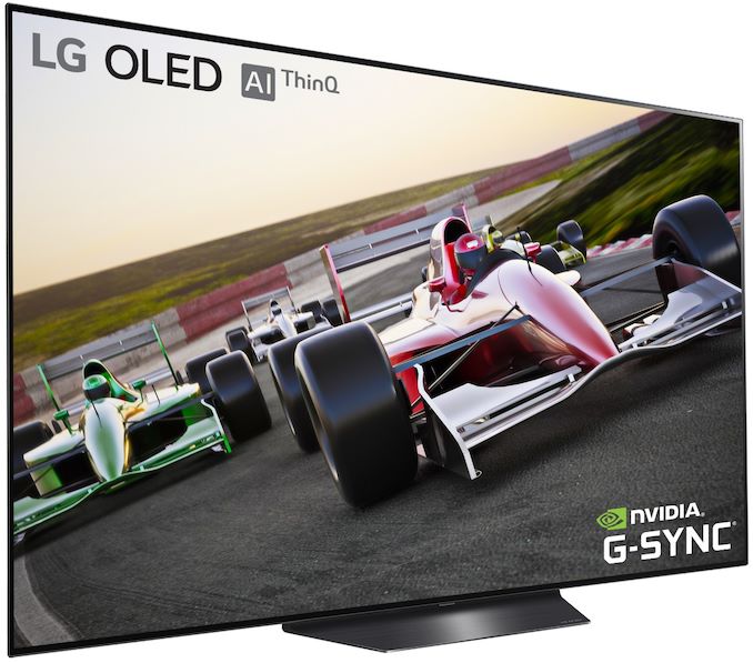
- NVIDIA To Officially Support VESA Adaptive Sync (FreeSync) Under “G-Sync Compatible” Branding
- GIGABYTE’s Aorus CV27Q Curved ‘Tactical’ Monitor: 165 Hz QHD With FreeSync 2
- HDMI Forum Demonstrates HDMI 2.1 VRR Capabilities on Samsung TV
Source: LG, NVIDIA
More...
-
11-01-19, 05:57 PM #10017
Anandtech: Google To Acquire Fitbit for $2.1 Billion
Google on Friday announced that that it had reached an agreement to buy Fitbit, a leading maker of advanced fitness trackers. Google stressed that data obtained and processed by Fitbit’s devices will remain in appropriate datacenters and will not go elsewhere.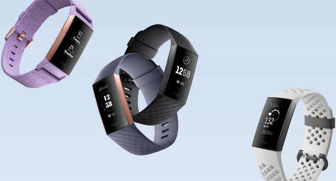
Under the terms of the agreement, Google will pay $2.1 billion in cash, valuing the company at $7.35 per share. In accordance with the deal, Google will become the sole owner of Fitbit, owning its IP and handling all hardware and software development and distribution.
The takeover of Fitbit is the latest step in Google’s ongoing strategy to make its Android platform more attractive to consumers. Fitbit has more than 28 million of active users, and while the company is far from the lion's share of the wearables market, it has a significantly bigger presence than the small number of Wear OS devices that Google's partners have been able to sell.
Overall, this is is the second major wearables-related acquisition for Google this year. Earlier this year the company also bought technology and R&D personnel from watch maker Fossil.
James Park, co-founder and CEO of Fitbit, said the following:
“Google is an ideal partner to advance our mission. With Google’s resources and global platform, Fitbit will be able to accelerate innovation in the wearables category, scale faster, and make health even more accessible to everyone. I could not be more excited for what lies ahead.”
The transaction will be closed in 2020 and from there expect Google to integrate Fibit’s IP into the Android platform.
Related Reading:
- Fitbit Shifts Production Away from China
- Google Announces The Pixel 4 and Pixel 4 XL: The 2019 Pixels
- Google Acquires Smartwatch Tech and R&D Personnel from Fossil
Source: Google/Fitbit press release
More...
-
11-04-19, 10:02 AM #10018
Anandtech: Intel Launches Xeon-E 2200 Series for Servers: 8 Cores, up to 5.0 GHz
The Xeon-E family from Intel replaced the Xeon E3-1200 parts that were found common place in a lot of office machines and small servers. The Xeon E parts are almost direct analogues of the current leading consumer processor hardware, except with ECC memory support and support for vPro out of the box. Today’s launch is a secondary launch, with Intel having released the Xeon-E 2200 series some time ago for the cloud market, but this launch marks general availability for consumers and the small-scale server market.
More...
-
11-04-19, 10:02 AM #10019
Anandtech: Samsung Confirms Custom CPU Development Cancellation
The fate of Samsung's custom CPU development efforts has been making the rounds of the rumour mill for almost a month, and now we finally have confirmation from Samsung that the company has stopped further development work on its custom Arm architecture CPU cores. This public confirmation comes via Samsung’s HR department, which last week filled an obligatory notice letter with the Texas Workforce Commission, warning about upcoming layoffs of Samsung’s Austin R&D Center CPU team and the impending termination of their custom CPU work.
The CPU project, said currently to be around 290 team members large, started off sometime in 2012 and has produced the custom ARMv8 CPU microarchitectures from the Exynos M1 in the Exynos 8890 up to the latest Exynos M5 in the upcoming Exynos 990.
Over the years, Samsung’s custom CPU microarchitectures had a tough time in differentiating themselves from Arm’s own Cortex designs, never being fully competitive in any one metric. The Exynos-M3 Meerkat cores employed in the Exynos 9810 (Galaxy S9), for example, ended up being more of a handicap to the SoC due to its poor energy efficiency. Even the CPU project itself had a rocky start, as originally the custom microarchitecture was meant to power Samsung’s custom Arm server SoCs before the design efforts were redirected towards mobile use.
In a response to Android Authority, Samsung confirmed the choice was based on business and competitive merits. A few years ago, Samsung had told us that custom CPU development was significantly more expensive than licensing Arm’s CPU IP. Indeed, it’s a very large investment to make in the face of having the up-hill battle of not only to designing a core matching Arm’s IP, but actually beating them.
Beyond the custom CPU’s competitiveness, the cancellation likely is tied to both Samsung’s and Arm’s future CPU roadmaps and timing. Following Deimos (Cortex-A77) and Hercules (Cortex-A78?), Arm is developing a new high-performance CPU on the new ARMv9 architecture, and we expect a major new v9 little core to also accompany the Matterhorn design. It’s likely that Samsung would have had to significantly ramp up R&D to be able to intercept Arm's ambitious design, if even possible at all given the area, performance, and efficiency gaps.
In practice, the end result is bittersweet. On one hand, the switch back to Cortex-A CPUs in future Exynos flagship SoCs should definitely benefit SLSI’s offerings, hopefully helping the division finally achieve SoC design wins beyond Samsung’s own Mobile division – or dare I hope, even fully winning a Samsung Galaxy design instead of only being a second-source alongside Qualcomm.
On the other hand, it means there’s one less custom CPU development team in the industry which is unfortunate. The Exynos 990 with the M5 cores will be the last we’ll see of Samsung’s custom CPU cores in the near future, as we won't be seeing the in-development M6. M6 was an SMT microarchitecture, which frankly quite perplexed me as a mobile targeted CPU – I definitely would have wanted to see how that would have played out, just from an academic standpoint.
The SARC and ACL activities in Austin and San Jose will continue as Samsung’s SoC, AI, and custom GPU teams are still active, the latter project which seems to be continuing alongside the new AMD GPU collaboration and IP licensing for future Exynos SoCs.
Related Content:- Samsung Announces Exynos 990: 7nm EUV, M5, G77, LPDDR5 Flagship SoC alongside Exynos 5123 5G Modem
- AMD and Samsung's GPU Licensing Deal: A New Era of Collaboration?
- The Samsung Galaxy S10+ Snapdragon & Exynos Review: Almost Perfect, Yet So Flawed
- Hot Chips 2018: Samsung’s Exynos-M3 CPU Architecture Deep Dive
- The Samsung Galaxy S9 and S9+ Review: Exynos and Snapdragon at 960fps
- Hot Chips 2016: Exynos M1 Architecture Disclosed
More...
-
11-04-19, 11:42 AM #10020
Anandtech: Dells Latitude 7220 Rugged Extreme Tablet Gets Quad-Core CPUs & 1000-Nits
Dell has introduced a new version of its high end 12-inch Latitude Rugged Extreme tablet, the Latitude 7220 Rugged Extreme. Like other ruggedized PCs, the new 7220 is designed to reliably work in harsh environments, offering against scapes, drops, and material ingresses of all kinds. At a high level, Dell's latest ruggedized tablet largely carries over their earlier designs – making it compatible with 'most' of the accessories developed for them – but now it has been upgraded to a quad-core Intel Core 8th Generation CPU, a 1000 nits display, as well as the latest in connectivity technologies.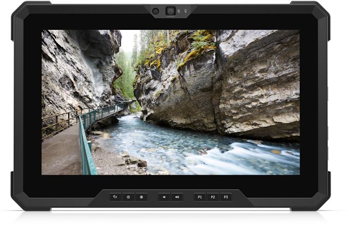
Dell has a history of offering fully-rugged tablets that goes back to 2015, and with the Latitude 7220 RE they are now on their third generation tablet. Just like its predecessors, the Latitude 7220 Rugged Extreme tablet comes in the MIL-STD-810G-certified 24-mm thick chassis designed to withstand operating drops, thermal extremes (-29°C to 63°C (20°F to 145°F), dust, sand, humidity, blowing rain, vibration, functional shock and all other kinds of physical impact. The tablet is also MIL-STD-461F certified, meaning that the Latitude 7220 RE is both designed to avoid leaking electromagnetic interference, as well as being able to resist it.
Because of the significant chassis bulk required meet the durability requirements for a ruggedized device, the Latitude 7220 Rugged Extreme is neither small nor light; the device weighs in 1.33 kilograms, which is comparable to a full-blown 13.3-inch notebook. In fact, the new model is 60 grams heavier than the previous-generation Latitude 7212 Rugged Extreme.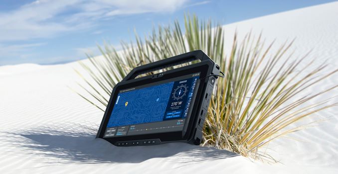
From a technology perspective, one of the key improvements with the Latitude 7220 RE is its new display panel, which offers a peak luminance of 1000 nits and should be bright enough to provide decent image quality even under direct sunlight. The brightness of the screen can now be regulated on the front panel of the tablet, which should be rather convenient. Meanwhile, the tablet no longer has a dedicated Windows button, but the latter is still present on Dell’s optional IP65-rated keyboard cover with kickstand.
Under the hood of the new tablet is Intel’s 8th Generation Core i3/i5/i5 (Whiskey Lake) processor, which offers two or four cores along with Intel’s UHD Graphics 630. Depending on exact tablet SKU, that CPU can be accompanied by 8 GB or 16 GB of LPDDR3 memory and a PCIe 3.0 x4-based Class 35 or Class 40 M.2 SSD, with capacities ranging from 128 GB to 2 TB. The system can be powered by two hot-swappable batteries, each with a 34 Wh capacity (by default, the system includes only one), though Dell isn't promoting specific battery life figures since they expect the tablet's customers to have a pretty varied range of use cases.
Meanwhile, Dell's latest ruggedized tablet has also received a communications upgrade. The tablet not only offers Wi-Fi 5/6 and Bluetooth (which can be hardware disabled for military-bound devices), but also can include an optional Qualcomm Snapdragon X20 4G/LTE modem, as well as a FirstNet module to access networks for first responders.
As for wired I/O, the Latitude 7220 Rugged Extreme includes a USB 3.1 Type-C connector that can be used for charging and external display connectivity, a USB 3.0 Type-A port, an optional micro RS-232 port, a POGO connector for the keyboard, and a 3.5-mm audio jack for headsets. The tough tablet also features rear and front cameras, an SD card reader, an optional contactless smart card reader, as well as a touch fingerprint sensor. Meanwhile, notably unlike its predecessor, the 7220 no longer includes a GbE port, VGA, HDMI, nor some other legacy I/O options.
As far as security is concerned, Dell’s Latitude 7220 Rugged Extreme can be configured to cover all the bases. The tablet has a fingerprint reader, Dell’s ControlVault advanced authentication, Intel vPro remote management, a TPM 2.0 module, optional encryption for SSDs, and NIST SP800-147 secure platform.
The Dell Latitude 7220 Rugged Extreme tablet is now available from Dell starting at $1,899.Specifications of the Dell Latitude 12 Rugged Extreme Tablets Latitude 12 7212
2017Latitude 7220
2019LCD Diagonal 11.6" 11.6" Resolution 1920×1080 Features Outdoor-readable display with gloved multi-touch AG/AR/AS/Polarizer and Gorilla Glass Brightness: 1000 cd/m²
Outdoor-readable, anti-glare, anti-smudge, polarizer, glove-capable touchscreenCPU Dual-Core 7th Gen Intel Core i5 CPUs (Skylake-U)
Dual-Core 7th Gen Intel Core i3/i5/i7 CPUs (Kaby Lake-U)Intel Core i7-8665U: 4C/8T vPro Intel Core i5-8365U: 4C/8T vPro
Intel Core i3-8145U: 2C/4TGraphics Intel HD Graphics 520/620
(24 EUs)Intel UHD Graphics 630
(24 EUs)RAM 8 GB or 16 GB LPDDR3 8 GB or 16 GB LPDDR3-2133 Storage 128 GB SATA Class 20 SSD
256 GB SATA Class 20 SSD Opal 2.0 SED
256 GB SATA Class 20 SSD
256 GB PCIe NVMe Class 40 SSD Opal 2.0 SED
512 GB SATA Class 20 SSD Opal 2.0 SED
512 GB SATA Class 20 SSD
512 GB PCIe NVMe Class 40 SSD
1 TB SATA Class 20 SSD
1 TB PCIe NVMe Class 40 SSDM.2 PCIe 3.0 x4 SSDs:
Class 35: 128 GB;
Class 40: 256 GB, 512 GB, 1 TB, 2 TB;
Class 40 SED: 256 GB, 512 GB, 1 TB.Wireless Wi-Fi,
Bluetooth optionsWireless LAN Options:
Intel Dual Band Wireless-AC 8265 with Bluetooth 4.2 + vPro Mobile broadband
Intel Dual Band Wireless-AC 8265 + No Bluetooth 4.2 Wireless Card
Qualcomm QCA61x4A 802.11ac Dual Band (2x2) Wireless Adapter+ Bluetooth 4.1Wireless LAN Options:
Intel Wireless-AC 9560, 2x2, 802.11ac with Bluetooth 5.0
Intel Wi-Fi 6 AX200, 2x2, 802.11ax with MU-MIMO, Bluetooth 5.0
Intel Wi-Fi 6 AX200, 2x2, 802.11ax with MU-MIMO, without BluetoothMobile Broadband
(optional)Qualcomm Snapdragon X7 LTE-A for Win 10 (DW5811e Gobi5000) for Worldwide (Windows 7 and 10 options)
Qualcomm Snapdragon X7 LTE-A for Win 10 (DW5811e Gobi5000) for AT&T (Windows 7 and 10 options)
Qualcomm Snapdragon X7 LTE-A for Win 10 (DW5811e Gobi5000) for Verizon (Windows 7 and 10 options)
Qualcomm Snapdragon X7 LTE-A for Win 10 (DW5811e Gobi5000) for Sprint (Windows 7 and 10 options)
Dell Wireless 5816e multi-mode Gobi 5000 4G LTE WAN Card (Japan/ANZ only)DW5821E Qualcomm Snapdragon X20 4G/LTE Wireless WAN card for AT&T, Verizon, Sprint GPS Dedicated u-blox NEO-M8 GPS card Additional Dual RF-passthough (Wi-Fi and mobile broadband), Near field communication (NFC) ? USB 3.1 1 × USB 3.0 Type-C w/ DP, PD 3.0 1 × USB 3.0 Type-ACameras Front Front-facing camera 5 MP RGB + IR FHD webcam with privacy shutter Back Rear-facing camera with flash LED 8 MP rear camera with flash and dual microphone Security Optional Security includes:
TPM 2.0;
ControlVault advanced authentication;
Dell Security Tools;
Dell data protection encryption;
Contactless SmartCard reader; Fingerprint reader.Steel reinforced cable lock slot
Optional Security includes:
TPM 2.0;
ControlVault advanced authentication;
Dell Security Tools;
Dell data protection encryption
Contactless/Contacted SmartCard reader;
Fingerprint reader;
NIST SP800-147 secure platform;
Dell Backup and Recovery.Other I/O TRRS audio jack, micro RS-232 (optional), POGO, SD Card reader, etc. Battery 34 Wh Primary battery 34 Wh Primary
(ExpressCharge)
34 Wh Secondary (optional?)Dimensions Width 312 mm | 12.3 inch 312.2 mm | 12.29 inch Height 203 mm | 8 inch 203 mm | 8 inch Thickness 24 mm | 0.96 inch 24.4 mm | 0.96 inch Weight 1270 grams (tablet) 1330 grams (tablet) Operating System Microsoft Windows 10 Pro 64 Bit
Microsoft Windows 10 Pro with Windows 7 Professional Downgrade (64 bit) - Skylake CPU requiredMicrosoft Windows 10 Pro 64 Bit Regulatory and Environmental Compliance MIL-STD-810G Transit drop (48”/1.22m; single unit; 26 drops), operating drop (36”/0.91m), blowing
rain, blowing dust, blowing sand, vibration, functional shock, humidity, salt fog, altitude, explosive atmosphere,
thermal extremes, thermal shock, freeze/thaw, tactical standby to operational.Operating thermal range -20°F to 145°F (-29°C to 63°C) Non-operating thermal range -60°F to 160°F (-51°C to 71°C) IEC 60529 ingress protection IP-65 (dust-tight, protected against pressurized water) Hazardous locations ANSI/ISA.12.12.01 certification capable (Class I, Division 2, Groups A, B, C,D),
CAN/CSA C22.2ANSI/ISA.12.12.01 certification capable (Class I, Division 2, Groups A, B, C,D) Electromagnetic interference MIL-STD-461F certified MIL-STD-461F and MIL-STD-461G Optional Accessories Dell Desktop Dock for the Rugged Tablet,
Dell Dock WD15,
Dell Power Companions,
Kickstand and Rugged RGB Backlit Keyboard cover,
Shoulder Strap,
Soft and Rigid Handle options,
Chest Harness,
Cross Strap, Active Pen,
Backpack Modules,
Dell monitors,
Dell Wireless Keyboard and MouseRugged Tablet Dock
Keyboard with Kickstand
Havis Vehicle Dock
PMT Vehicle Dock
Gamber-Johnson Vehicle Dock
Carrying accessories
Scanner module
Extended I/O module
Dell monitors (with USB-C or over a USB-C-to-DP adapter)
Dell wireless keyboard and micePrice Starting at $1,899
Related Reading:
- Dell Launches Three Rugged Latitude Laptops with up to 1000-nit Displays
- Dell Latitude 12 Updated: Rugged Tablet Gets Faster CPU, FHD LCD, Lower Weight, USB-C
- Dell Announces Latitude Rugged Extreme 12 and 14 Laptops
Source: Dell
Some images are made by Getty Images and distributed by Dell
More...


 Quote
QuoteThread Information
Users Browsing this Thread
There are currently 22 users browsing this thread. (0 members and 22 guests)


Bookmarks