

Results 10,091 to 10,100 of 12096
Thread: Anandtech News
-
11-29-19, 11:32 AM #10091
Anandtech: Spotted at Supercomputing 2019: A 256 GB Gen-Z Memory Module
As a millennial, everything in the media that ‘Gen Z’ does often gets lumped into the millennial category. Thankfully there’s another type of Gen-Z in the world: the cache coherent memory-semantic standard. Where standards like CXL are designed to work inside a node, CXL is meant to work between nodes, providing a switched fabric or a point-to-point connectivity for memory, storage, accelerators, and even other servers.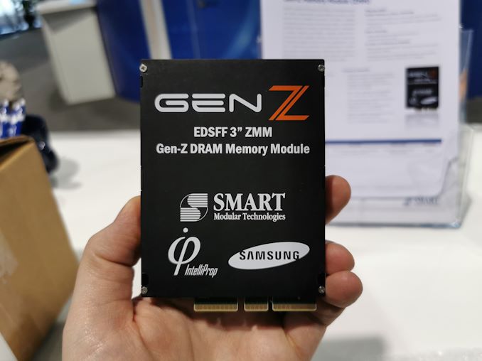
Earlier this year we saw the announcement of a Gen-Z switch which provides a fabric backbone to which hardware can be connected. The switch allows for fabric management, switching, routing, and security, and allows hardware configuration mixes of storage, compute, and accelerators. We found one such add-on at this year’s Supercomputing: the ZMM, or Gen-Z Memory Module.
What we had in front of us was actually a dummy unit for show purposes, but it is a 3-inch wide memory device that adds additional distributed memory to the network such that different nodes can take advantage of it when needed. Inside is 256 GB of DRAM, providing 30 GB/s bandwidth through the Gen-Z interface: that’s the equivalent of dual channel DDR4-1866. The total latency is listed as 400 ns which is an order of magnitude slower than main memory. Ultimately this is slower than traditional memory-controller supported DRAM, but aims to be faster than network attached storage.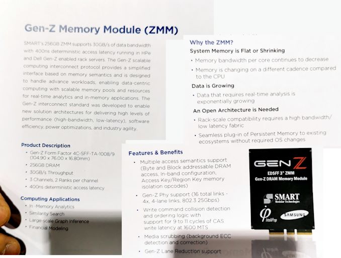
With these modules, ultimately the goal of Gen-Z is to have a 4U unit in a rack that customers can install any number of memory modules, storage drives, accelerators, or other compute resources, without worrying about exactly where they are in the system or how the system can access them. The Gen-Z consortium is aiming for ‘rack-scale compatibility’, and wants to be able to make these rack-level adjustments seemless to existing ecosystems without OS changes.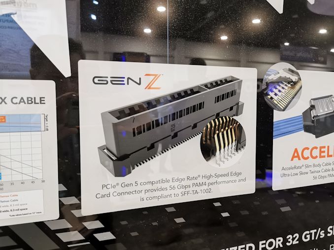
We also saw marketing for a PCIe Gen 5.0 compatible Gen-Z Connector
Related Reading- Gen-Z PHY Specification 1.1 Published: Adds PCIe 5.0, Gen-Z 50G Fabric
- Hot Chips 31 Live Blogs: Gen-Z Chipset for Exascale Fabric
More...
-
11-29-19, 11:32 AM #10092
Anandtech: Panasonic to Sell Semiconductor Business to Nuvoton
Panasonic has announced plans to almost completely withdraw from semiconductor business and sell all of its related assets to Taiwan-based Nuvoton Technology, a wholly owned subsidiary of Winbond Electronics. Under the terms of the deal, Nuvoton will get Panasonic’s semiconductor manufacturing assets, chip & product development units, contracts, and sales assets for about $250 million. Following the transaction, the only semiconductor-related property that Panasonic will have will be its 20% stake in Socionext.
Panasonic started its semiconductor business back in 1957 and was once a leading designer and maker of chips. As competition in the industry intensified early this decade, the company adopted an asset light strategy and started to gradually withdraw from both the development and manufacturing of semiconductors. In 2014, it sold a 51% stake in its chip manufacturing assets (consisting of one 300-mm and two 200-mm fabs) to TowerJazz, then Panasonic sold off its assembly/test facilities to UTAC. Finally, the company outsourced production of advanced SoCs to Intel Custom Foundry, which symbolized their withdrawal from development of leading-edge process technologies.
It did not take long for the company to realize that the design of complex SoCs was getting too expensive, which is why in March of 2015 it transferred its SoC development assets to Socionext, a joint venture between the Development Bank of Japan, Fujitsu, and Panasonic. Recently, Panasonic sold its diode and transistor business to Rohm Semiconductor. All told, Panasonic's chip business has been on a downward spiral for quite a while now.
By contrast, Nuvoton, which was established in 2008 by Winbond to produce microcontrollers, power management ICs, and other similar devices, has been quite a success. It has numerous clients and it looks like its 200-mm fab is not enough for the company. Under the terms of the agreement with Panasonic and TowerJazz, through acquisition of Panasonic Semiconductor Solutions Co. (PSCS) it will get all three Japanese fabs which originally belonged to Panasonic. Meanwhile, the sum that Nuvoton will pay to TowerJass is unknown.
Furthermore, Nuvoton will get Panasonic’s business and R&D operations related to power-management ICs, sensors (for smartphones, vehicles, and various types of cameras) and other types of products by taking over Panasonic Industrial Devices Systems & Technology (PIDST), Panasonic Industrial Devices Engineering (PIDE), and Panasonic Semiconductor Suzhou (PSCSZ) companies.
As a result of the business transaction, Nuvoton will own four semiconductor manufacturing facilities: one 300-mm fab and three 200-mm fabs. Moreover, it will get a rich portfolio of products, customers, and contracts. However it will also be inheriting the debts of the aforementioned companies. Ultimately this will allow Panasonic to exit the semiconductor business, improving its own financial position.
Related Reading:
- Panasonic to Cease LCD Production by 2021
- MWC 2017: Panasonic Demonstrates Store Window as a Transparent Screen
- Panasonic Develops IPS Panel with 1,000,000:1 Contrast Ratio, 1000 Nits Brightness
- SMIC Begins Volume Production of 14 nm FinFET Chips: China’s First FinFET Line
- Sony to Build New Fab to Boost CMOS Sensor Output
Sources: Panasonic, Nuvoton. Taipei Times, Reuters
More...
-
11-29-19, 02:58 PM #10093
Anandtech: Two Phase Immersion Liquid Cooling at Supercomputing 2019
It would now appear we are saturated with two phase immersion liquid cooling (2PILC) – pun intended. One common element from the annual Supercomputing trade show, as well as the odd system at Computex and Mobile World Congress, is the push from some parts of the industry towards fully immersed systems in order to drive cooling. Last year at SC19 we saw a large number of systems featuring this technology – this year the presence was limited to a few key deployments.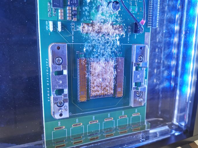
More...
-
12-01-19, 09:10 AM #10094
Anandtech: Junk or Treasure? We Tested Amazons Cheapest Black Friday Desktop PC, onl
Some Black Friday deals are wild. A store might offer only a couple of units of a particular TV, discounted by 66%. There might be a few pieces of a flagship smartphone at your local electronics store at half price. These are designed to entice customers through the door, and if you’re brave enough, ensure the cold for up to 12 hours to get that bargain of the year. But one of the key observations about looking at Amazon’s Computing and Components section every Black Friday, particularly this year, is that most of the discounts are for complete trash. After the headline external storage discounts, it’s just page after page of USB cables and smartphone holders. But one thing did catch my eye: an entire PC, for only £57 / $61! How can an entire x86 desktop PC be sold for so little? We did the only thing worth doing: we purchased it.
More...
-
12-02-19, 11:48 AM #10095
Anandtech: BOE to Triple Production of Smartphone AMOLED Panels
BOE has outlined a new set of aggressive plans to expand production of AMOLED display panels for mobile devices next year. The company has reasons to be optimistic as it is adding two AMOLED production lines to its fleet, yet their ramp to full capacity is something that remains to be seen.Meanwhile the company has also noted that LCD panel supply is outpacing demand, which makes AMOLED a much more lucrative market at this time..
At BOE’s annual Innovation Partner Conference last week, Chen Yanshun, chairman of the company, said that the company would more than triple production of AMOLED display panels for smartphones (and similarly-sized devices) as early as next year, allowing it to ship upwards of 70 million units. The aggressive goals come as the company is in the process of greatly expanding its manufacturing capacities.
BOE started production of AMOLED panels for mobile devices in October 2017 at its 6th Generation plant in Chengdu, Sichuan province. This factory supplies displays to more than 10 smartphone makers, including Huawei, Oppo, and Vivo. At present, this is the BOE’s only fully-ramped AMOLED line.
The company’s second 6th Generation AMOLED plant in Mianyang, Sichuan province, started mass production of panels in July 2019. The facility yet has to ramp up to its full capacity and it is unclear how many panels it is set to make this year. Meanwhile, BOE says that it will produce around 20 million AMOLED panels this year.
BOE started construction of its third 6th Generation AMOLED manufacturing line in Chongqing last year, so expect it to start production sometimes in 2020, taking time to ramp up to peak production.
Once all three of BOE’s AMOLED production facilities are fully ramped, should be able to get close to their goals. Though whether they can hit (and sell) 70 million panels a year is definitely an ambitious target. But even if they don't hit 70 million, such an aggressive expansion of AMOLED production capacities will still be very welcome in the market, as the additional capacity will help to further push down display prices.
Related Reading:
- JOLED Starts Trial Production of Printed OLED Sheets at 5.5G Plant
- LG's New 55+ inch OLED Plant in China Opens: Over 1m+ per Year
- LG to Start Production of OLEDs in China Next Month, Set to Double OLED Output
- AU Optronics OLED Displays: A New Foldable + A New 17.3-Inch 4K120
- Samsung Mulls Suspending South Korea LCD Plant Due to Oversupply
Sources: China Daily, CDRInfo, OLED-Info
More...
-
12-02-19, 02:39 PM #10096
Anandtech: Toshiba to Expand HDD Production: 20 TB & 10-Platter Drives ?oming
While hard drive sales on a unit basis have continued to decline, the drop hasn't been consistent across all segments of the market. In particular, high capacity drives for hyperscalers and other hosts continue to be a hot commodity, as their data storage needs continue to grow and there are few other alternatives. As such, Toshiba has announced that the company will actually be increasing its HDD production capacity, expanding one of its plants in Philippines to increase output of high-end helium-filled enterprise and nearline HDDs. The company is confident of its roadmap (and growing demand for its products) which includes numerous promising products and technologies.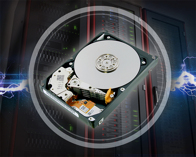
The overall broad shift in HDD demand from lower capacity client to high capacity nearline drives comes as Toshiba finds itself on the outside looking in. The company’s sales mix is dominated by client HDDs, with enterprise drives accounting for about a third of it. So while Toshiba controls about 36% of the global mobile HDD shipments, it only has around 17% of the enterprise/nearline market. As a result, Toshiba is looking to make changes to capture more of the nearline market.
At its Investors Day last month, Toshiba outlined plans to radically increase the share of enterprise/nearline HDDs in its product mix in FY2021 (starts on April 1, 2021), shifting away from client drives and towards nearline drives. Overall, the company set itself a goal to capture an ‘over 20%’ share of the global enterprise/nearline HDD market while maintaining its share of the client HDD market at around 25%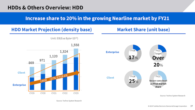
To reach its new goals, Toshiba not only needs to ramp up production, but it will need to ensure it has competitive pricing and technology as well. This means the company needs to continue to invest in developing leading-edge high-capacity nearline drives for hyperscale datacenters, while at the same time keeping prices in check so that they are priced competitively for the small and mid-sized datacenter market. As well, Toshiba will have to focus on client issues, such as improving its customer support as well as collaborating more with Chinese datacenter clients.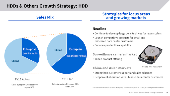
On the product side of things, Toshiba has a rather solid roadmap. Earlier this year the company confirmed that it would use shingled magnetic recording (SMR) and energy assisted magnetic recording (EAMR) technologies (e.g., MAMR, HAMR) to boost areal density. In addition to that, the company’s roadmap now officially includes drives with 10 platters (up from nine today). Which to offer some context, a 10-platter design using the highest-capacity platters available today would enable a 22 TB HDD. Though it bears mentioning that adding a 10th platter to existing drives is not a trivial task (i.e. how do you fit it in?), so Toshiba isn't disclosing when they expect to have their 10-platter design ready.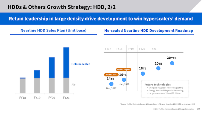
In the meantime, the company’s roadmap includes a 20 TB HDD as soon as FY2021. And, going forward, all of Toshiba's leading-edge hard drives will be helium-filled.
The big challenge – as is often the case – is on the manufacturing side of matters. Toshiba’s current capacity to build helium-filled devices in its Carmelray Industrial Park plant is somewhat limited, so the company needs to expand these production lines to meet demands it is going to face in the coming years. It's fitting then that even Toshiba is being a bit cautious here, holding off on disclosing specific production goals for helium drives.
Related Reading:
- Toshiba's HDD Tech Roadmap: A Mix of SMR, MAMR, TDMR, and HAMR
- 18 TB HDDs: Toshiba Collaborates with Showa Denko for MAMR HDDs
- Toshiba at CES 2019: World’s First 16 TB TDMR HDD Debuts
- Toshiba Launches 12 TB and 14 TB HDDs for Desktops and NAS
- Demand for HDD Storage Booming: 240 EB Shipped in Q3 2019
- Shipments of PC Hard Drives Predicted to Drop By Nearly 50% in 2019
- Seagate to Shut Down One of Its Largest HDD Assembly Plants
- Western Digital to Shut Down HDD Manufacturing Facility, Increase Production of SSDs
Source: Toshiba
More...
-
12-02-19, 02:39 PM #10097
Anandtech: AWS Designing a 32-Core Arm Neoverse N1 CPU for Cloud Servers
Amazon Web Services’s CPU design unit is working on a new multi-core processor for AWS servers. The new CPU is said to use Arm’s new Neoverse N1 architecture and would feature a considerably higher core-count when compared to AWS’s first-generation Graviton processor, which should result in a significant performance increase.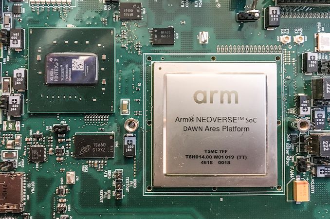
The yet-to-be-named AWS CPU will be based on Arm’s Neoverse N1 microarchitecture and will integrate as many as 32 cores, according to Reuters, which cites two sources with knowledge of the matter. The chip will also be able to connect to various special-purpose accelerators using a ‘fabric’ interface to greatly speed up certain workloads.
On a high level, the Neoverse N1 (aka Ares) to a large degree resembles Arm’s consumer-oriented Cortex-A76 microarchitecture: a 4-wide fetch/decode machine with a pipeline depth of only 11 stages that can reduce itself to 9 when needed. Meanwhile, the Neoverse N1 is designed to run at relatively high frequencies to provide maximum single-thread performance, it has a different cache architecture (coherent, with 1 MB L2 option, yet caches are technically not a part of the microarchitecture per se), and some other enhancements. Overall, with the Neoverse N1 Arm is looking at clocks of up to 3.1 GHz and a ~100 W TDP per SoC.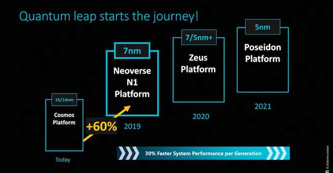
Readers who are interested to find out more about Arm’s Neoverse N1 platform can read our coverage from earlier this year, but the key thing in the context of the newly released information is that AWS continues to believe in custom Arm-based processors for servers and would be among the first adopters of the Neoverse N1. As noted above, the microarchitecture and the platform were optimized for cloud server workloads from the ground up, so with with further customization from Amazon, the 32-core processor promises to offer rather serious performance in applications that it was designed for. Will these CPUs challenge AMD’s Rome or Intel’s Cascade Lake? Probably not, but the importance of custom chips is their ability to offer the right total cost of ownership and sufficient performance, not win all the benchmarks.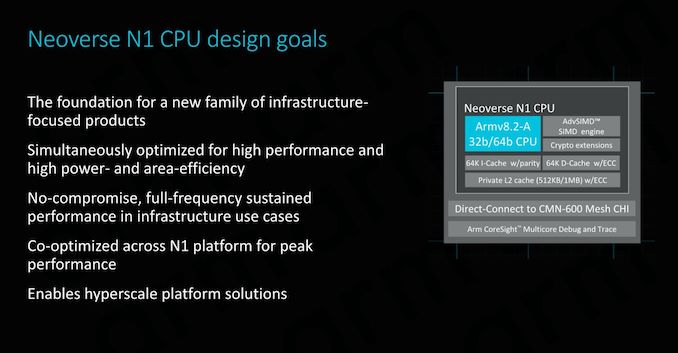
Related Reading:
- Arm Announces Neoverse N1 & E1 Platforms & CPUs: Enabling A Huge Jump In Infrastructure Performance
- GIGABYTE's Cavium ThunderX2 Systems: 1U R181-T90 and 2U R281-T91
- Assessing Cavium's ThunderX2: The Arm Server Dream Realized At Last
- GIGABYTE's ThunderXStation with Dual Cavium ThunderX2 Arm SoCs
- Investigating Cavium's ThunderX: The First Arm Server SoC With Ambition
- Marvell Completes Acquisition of Cavium, Gets CPU, Networking & Security Assets
- Amazon AWS Offers Another AMD EPYC-Powered Instance: T3a
- Amazon Offers More EPYC: M5ad & R5ad Instances
Source: Reuters
More...
-
12-02-19, 07:03 PM #10098
Anandtech: Japan Display Develops 1.6-Inch Micro LED Display Module: 265 PPI & 3,000
Japan Display Inc. (JDI) announced this week that it has completed development of its first Micro LED module. The prototype of the Micro LED module, which is a potential building block for next generation displays and TVs, offers a 265 PPI pixel density. JDI will be demonstrating the module at Fintech Japan 2019 later this week.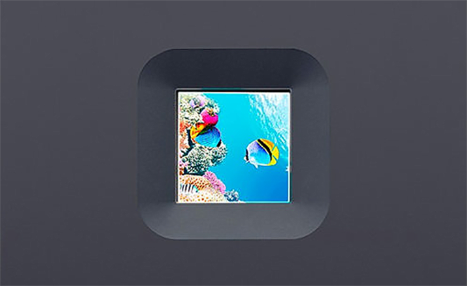
JDI’s Micro LED display prototype is a square module with a 1.6-inch diagonal, and offers a resolution of 300×300 pixels along with a maximum brightness of 3,000 nits. The prototype uses gallium nitride LED chips developed by glo (a Micro LED pioneer) and JDI’s LTPS backplane.
As part of the development process for Micro-LED displays, the hope is that display makers can assemble full-sized displays by building them out of individual modules such as JDIs. A modular approach not only offers more control over yields (as opposed to having to fail a full-sized panel over a flaw), but it would also allow manufacturers to easily support multiple resolutions and aspect ratios just by changing the number of modules. That said, being able to produce commercial panels in volume is still years off, and for now Japan Display has made significant progress just in completing their prototype module.JDI's Micro LED Display Module Prototype Feature Characteristic Screen size 1.6 inches Resolution 300×300×RGB Pixel density 265 PPI Luminance 3,000 cd/m² Viewing angle >178°
Micro LED technology is a promising candidate for higher-end displays and television that will be available three to four years down the road. The technology has virtually all the quality advantages that OLED has to offer (over LCD), including individually-controlled LEDs, high contrast, fast response times, and wide viewing angles. But equally important, it does not come with the major disadvantages that OLEDs are known for, such as off-axis color shifting and aging-related burn-in. There are many small companies working on Micro LED technology, but so far only a handful of actual displays/TVs manufacturers have showcased their Micro LED prototypes, and only two of them have started to commercialize this technology on a very small scale.
Related Reading:
- TCL Shows Off 132-Inch Micro LED 4K UHDTV: 24,000,000 Micro LEDs
- Samsung’s Micro LED Wall TVs Now Available: Up to 8K, Up to 292-Inches
- Sony’s Micro LED-Based Ultra-HD TVs Available to Consumers: 2K to 16K Resolutions, up to 790-Inches
- Chinese and Taiwanese Companies To Gain Controlling Stake of JDI
- Japan Display Develops VRM-100 VR Headset with 3DOF for Business Users
Source: Japan Display
More...
-
12-02-19, 09:24 PM #10099
Anandtech: Imagination Announces A-Series GPU Architecture: "Most Important Launch in
There are very few companies in the world able to claim a history in the graphics market dating back to the “golden age” of the 90’s. Among the handful of survivors of that era are of course NVIDIA and AMD (formerly ATI), but there is also Imagination Technologies. The company has been around since the early days of graphics accelerators and has seen a shifting industry. In the early to mid-2000’s the company moved away from the desktop space, instead focusing on offering GPU IP optimized for mobile devices.
Today, Imagination is announcing the brand-new “A-Series” GPU architecture, with the company describing the new release the biggest and most important IP launch in 15 years. All of which is quite a grandiose claim that we don’t often see in this industry. We’ll be going dive into the details of what the new “GPU of everything” brings to the table, and how Imagination to raise the bar in the highly competitive mobile GPU market.
More...
-
12-03-19, 11:25 AM #10100
Anandtech: Cherrys Secure Board 1.0 Encrypts Every Keystroke & Has Smart Card Reader
Security is one of the primary concerns for many organizations these days, so makers of hardware and software have been responding in-kind with new security features baked into their products. To that end, Cherry has introduced a new keyboard that has a smart card reader and can encrypt every keystroke to prevent keylogging.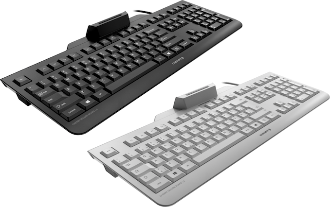
The Cherry Secure Board 1.0 is a classic looking black or white keyboard with inexpensive rubber dome switches (which Cherry calls LPK) that has an integrated Class 2 reader for ISO 7816 and ISO 14443 A/B-compliant smart cards as well as cards/tags with an RF/NFC interface. Such cards and tags are used by various government and corporate organizations to identify their employees using hardware means and control their access levels and actions. The board is FIPS-201 compliant.
The key feature of the Secure Board 1.0 is support for Secure Mode that verifies authenticity of the keyboard to its host PC with a special certificate and encrypts every key stroke when used in Secure Mode. According to Cherry, Secure Mode protects against BadUSB attacks, yet it does not explain how exactly other than saying that it blocks 'the standard keyboard channel'. At any rate, since Secure Mode encrypts every keystroke, it should make it impossible for keyloggers to intercept sensitive data and/or passwords.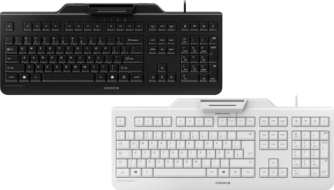
At this point, we can only speculate how Secure Mode works: it might prevent the OS from getting 03h (human interface device) descriptor from devices without a special certificate and thus infect the PC with a virus by executing preprogrammed keystrokes and/or running certain applications. Alternatively, it might prevent the OS from recognizing any unencrypted input from a keyboard.
The biggest limitation with Secure Mode at the moment is that it currently works only with clients running Linux, while Windows support is still under development. This pretty much limits usefulness of Secure Mode to a handful of corporate desktops, but considering the fact that Cherry is a German company and Linux is widely used in Germany, it's not as problematic as it may first appear for Cherry's home market.
Cherry has already started to sell its Secure Board 1.0 keyboards in Europe and the UK for €69.99 and £64.99 respectively. Versions with layout for Belgium, Germany, France, Italy, Spain, Switzerland, Nordic, and the UK are available. There are also black and white versions with the US layout (albeit with € symbol).
Related Reading:
- HP’s Endpoint Security Controller: More Details About A New Chip in HP Notebooks
- HP’s Security Push: Sure Sense & Endpoint Security Controller
- Synaptics' Next-Gen Fingerprint Sensor Security: The FS7600 Match-In-Sensor
- Synaptics Discusses Fingerprint Security and the Need For End-to-End Encryption
- Cherry Launches MC 4900 Mouse with Fingerprint Reader, 1375 DPI Sensor
- Cherry Announces the MW 4500 Mouse with 45° Palm Rest, 1200 DPI Sensor
Source: Cherry
More...


 Quote
QuoteThread Information
Users Browsing this Thread
There are currently 47 users browsing this thread. (0 members and 47 guests)


Bookmarks