

Results 10,451 to 10,460 of 12096
Thread: Anandtech News
-
03-24-20, 04:40 PM #10451
Anandtech: GOODRAM Announces Entry-Level PX500 SSDs: Bringing NVMe to Budget Drives
As more SSD manufacturers introduce their inexpensive NVMe PCIe drives, the market of entry-level SSDs is slowly but surely moving away from SATA altogether. Case in point this week is GOODRAM, yet another SSD manufacturer who is launching a family of entry-level NVMe SSDs that are priced to compete with their SATA counterparts.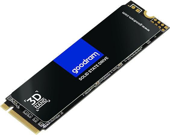
GOODRAM’s PX500-series SSDs are based on Silicon Motion’s SM2263XT controller and come with 256 GB, 512 GB, or 1 TB of usable 3D TLC NAND memory. The entry-level drives fully support modern SSD features like the NVMe 1.3a protocol, end-to-end data protection, L1.2 low power mode, and AES-256 encryption. What's also notable is that the manufacturer is specifically designing the M.2 2280 form-factor drives with laptop compatibility in mind; so rather than using a large metal heatsink, the drives are covered by a thin heat spreader made of plastic-like material so that they fit into the tight spaces afforded by laptops.
When it comes to performance, GOODRAM rates the new PX500-series SSDs for up to 2050 MB/s sequential read speeds, up to 1650 MB/s sequential write speeds, and up to 240,000/280,000 random read/write IOPS, which is in line with the capabilities of the controller and performance levels offered by competing drives.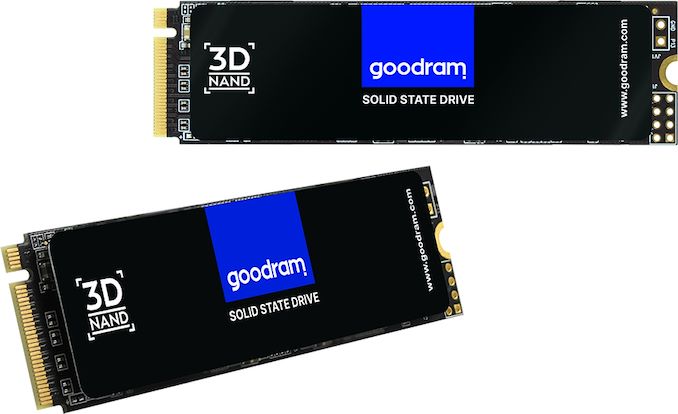
Wilk Electronik SA, the owner of the GOODRAM brand, has not announced official MSRPs for its PX500 SSDs, but the general principle here is that they are supposed to launch at prices that are close to those for M.2 SATA SSDs.General Specifications of GOODRAM's PX500 SSDs Capacity 256 GB 512 GB 1 TB Model Number SSDPR-PX500-256-80 SSDPR-PX500-512-80 SSDPR-PX500-01T-80 Controller Silicon Motion SM2263XT NAND Flash 3D TLC NAND Form-Factor, Interface M.2-2280, PCIe 3.0 x4, NVMe 1.3a Sequential Read 1850 MB/s 2000 MB/s 2050 MB/s Sequential Write 950 MB/s 1600 MB/s 1650 MB/s Random Read IOPS ~102K IOPS ~173K IOPS ~240K IOPS Random Write IOPS ~230K IOPS ~140K IOPS ~280K IOPS Pseudo-SLC Caching Supported DRAM Buffer No TCG Opal Encryption No Power Management L1.2 power mode support for ultra-low power consumption
Idle: ? W
Active: ? WWarranty 3 years MTBF 1,500,000 hours (?) TBW ? ? ? Additional Information Link Launch Price ? ? ?
Related Reading: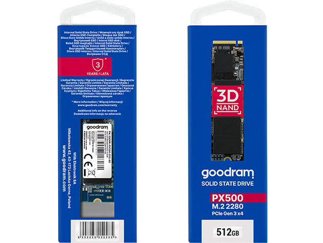
- Patriot Releases Cheap P300 M.2 PCIe SSDs: Two Products, Same Name
- Biostar Launches M700 SSDs: Entry-Level PCIe SSDs
- Team Group Unveils MP33 SSDs: Entry-Level PCIe Drives
- Mushkin’s Helix-L SSDs Available: Pushing the Price of 3D TLC
Source: GOODRAM
More...
-
03-25-20, 10:11 AM #10452
Anandtech: Samsung to Produce DDR5 in 2021 (with EUV)
Samsung is on track to start volume production of DDR5 and LPDDR5 memory next year using a manufacturing technology that will take advantage of extreme ultraviolet lithography (EUVL). In fact, Samsung has been playing with EUV-enabled DRAM fabrication process for a while and has already validated DDR4 memory with select partners.
To date, Samsung has produced and shipped a million of DDR4 DRAM modules based on chips made using the company’s D1x process technology that uses EUV lithography. These modules have completed customer evaluations, which proves that Samsung’s 1st Generation EUV DRAM technology enables to build fine circuits. Samsung’s D1x is an experimental EUVL fabrication process that was used to make experimental DDR4 DRAMs, though it will not be used any further, the company said.
Instead, to produce DDR5 and LPDDR5 next year, the company will use its D1a, a highly-advanced 14 nm-class process with EUV layers. This technology is expected to double per-wafer productivity (DRAM bit output) when compared to D1x technology, which indicates that it uses thinner geomtries. Samsung did not reveal whether its D1a also uses other innovations (in addition to EUVL), such as pillar cell capacitors and dual work function layers for buried wordline gates, as anticipated by analysts from TechInsights who believe that scaling DRAM cell transistors and capacitor structures offer limited capability to scale further from current levels.
Usage of EUVL will enable Samsung (and eventually other memory makers) to reduce (or eliminate) usage of multi patterning, which enhances patterning accuracy and therefore improves performance and yields. The latter will be beneficiary for production of high-performance high-capacity DDR5 chips as they are meant to increase both performance (up to DDR4-6400) and capacity (up to 32 Gbps). Samsung has not officially revealed how many EUV layers do its D1x and D1a process technologies use.Timeline of Samsung DRAM Milestones Date Milestone 2021 4th-gen 10nm-class (1a) EUV-based
16Gb DDR5/LPDDR5 mass productionMarch 2020 4th-gen 10nm-class (1a) EUV-based DRAM development September 2019 3rd-gen 10nm-class (1z) 8Gb DDR4 mass production June 2019 2nd-gen 10nm-class (1y) 12Gb LPDDR5 mass production March 2019 3rd-gen 10nm-class (1z) 8Gb DDR4 development November 2017 2nd-gen 10nm-class (1y) 8Gb DDR4 mass production September 2016 1st-gen 10nm-class (1x) 16Gb LPDDR4/4X mass production February 2016 1st-gen 10nm-class (1x) 8Gb DDR4 mass production October 2015 20nm (2z) 12Gb LPDDR4 mass production December 2014 20nm (2z) 8Gb GDDR5 mass production December 2014 20nm (2z) 8Gb LPDDR4 mass production October 2014 20nm (2z) 8Gb DDR4 mass production February 2014 20nm (2z) 4Gb DDR3 mass production February 2014 20nm-class (2y) 8Gb LPDDR4 mass production November 2013 20nm-class (2y) 6Gb LPDDR3 mass production November 2012 20nm-class (2y) 4Gb DDR3 mass production September 2011 20nm-class (2x) 2Gb DDR3 mass production July 2010 30nm-class 2Gb DDR3 mass production February 2010 40nm-class 4Gb DDR3 mass production July 2009 40nm-class 2Gb DDR3 mass production
In addition to revealing its EUV-related achievements, Samsung also said that in the second half this year its P2 fab near Pyeongtaek, South Korea, will begin operations later this year. Initially, the facility will ‘make next-generation premium DRAMs’.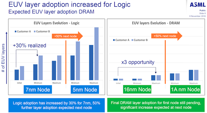
Jung-bae Lee, executive vice president of DRAM Product & Technology at Samsung Electronics, said the following: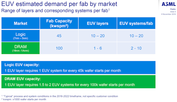
"With the production of our new EUV-based DRAM, we are demonstrating our full commitment toward providing revolutionary DRAM solutions in support of our global IT customers. This major advancement underscores how we will continue contributing to global IT innovation through timely development of leading-edge process technologies and next-generation memory products for the premium memory market."
Related Reading:
- Samsung Starts Mass Production at V1: A Dedicated EUV Fab for 7nm, 6nm, 5nm, 4nm, 3nm Nodes
- CES 2020: Micron Begins to Sample DDR5 RDIMMs with Server Partners
- Micron’s DRAM Update: More Capacity, Four More 10nm-Class Nodes, EUV, 64 GB DIMMs
- Keysight Reveals DDR5 Testing & Validation System
- SK Hynix Develops First 16 Gb DDR5-5200 Memory Chip, Demos DDR5 RDIMM
- Cadence & Micron DDR5 Update: 16 Gb Chips on Track for 2019
- Cadence and Micron Demo DDR5-4400 IMC and Memory, Due in 2019
Source: Samsung
More...
-
03-25-20, 12:23 PM #10453
Anandtech: The GIGABYTE MZ31-AR0 Motherboard Review: EPYC with Dual 10G
The workstation and server markets are big business for not only chip manufacturers such as Intel and AMD, but for motherboard vendors too. Since AMD's introduction of its Zen-based EPYC processors, its prosumer market share has been slowly, but surely creeping back. One example of a single socket solution available on the market is the GIGABYTE MZ31-AR0. With support for AMD's EPYC family of processors, the MZ31-AR0 has some interesting components including its 2 x SFP+ 10 G Ethernet ports powered by a Broadcom BCM57810S controller, and four SlimSAS slots offering up to sixteen SATA ports.
More...
-
03-25-20, 12:23 PM #10454
Anandtech: Intels new Single Customer Ice Lake Mobile CPUs: Are These in the Macbo
It was recently brought to our attention that three new Ice Lake CPUs were listed on Intel’s online ARK database of products: the Core i7-1060NG7, the Core i5-1030NG7, and the Core i3-1000NG4. These differ from the ‘consumer’ released products by having an ‘N’ in them, and specification-wise these CPUs have a slightly higher TDP along with a slightly higher base clock, as well as being in a smaller package. We reached out to Intel, but in the meantime we also noticed that the CPUs line up perfectly with what Apple is providing in its latest Macbook Air.
Intel’s Ice Lake family is the first generation of 10nm processors that the company has made widely available. We’ve covered Intel’s ups and downs with the 10nm process, and last year it launched Ice Lake as part of its 10th Generation Core family, focusing more on premium products that need graphics horsepower or AI acceleration. In the initial announcement, Intel stated that there would be nine different Ice Lake processors coming to market, however we learned that the lower-power parts would take longer to arrive.
These three new CPUs actually fall under that ‘lower power’ bracket, meaning they were meant to be coming out about this time, but are labelled differently to the processors initially announced. This is because these new CPUs are officially listed as ‘off-roadmap’, which is code for ‘not available to everyone’. Some OEMs, particularly the big ones like Apple, or sometimes HP and others, will make a request to Intel to develop a special version of their products just for them. This product is usually the same silicon as before, but binned differently, often to tighter constraints: it might differ in frequency, TDP, core count, or the way it is packaged. This more often happens in the server space, but can happen for notebooks as well, assuming you can order a larger amount.
These new CPUs are different because they have an ‘N’ in the name. This translates, in the case of the Core i7, to +1W on the TDP, +200 MHz on the base frequency, and a much smaller package size. They are all classified as Iris Plus graphics, and the G7 indicates 64 EUs while the G4 indicates 48 EUs. Interestingly the new CPUs have Intel’s TXT and Optane Memory Support disabled. Increasing the TDP by 11% and the base frequency by 20% is probably very reasonable – ultimately the TDP affects more for the sustained performance, for which customers that want custom versions are probably optimizing for quite well.Intel Ice Lake-Y Variants AnandTech 1060N
G71060
G71030N
G71030
G71000N
G41000
G4Cores / Threads 4 / 8 4 / 8 4 / 8 4 / 8 2 / 4 2 / 4 L3 Cache 8 MB 8 MB 6 MB 6 MB 4 MB 4 MB Base Freq (GHz) 1.20 1.00 1.10 0.80 1.10 1.10 Turbo Freq (GHz) 3.80 3.80 3.50 3.50 3.20 3.20 TDP 10 W 9 W 10 W 9 W 9 W 9 W LPDDR4X 3733 3733 3733 3733 3733 3733 GPU EUs 64 64 64 64 48 48 GPU Freq (MHz) 1100 1100 1050 1050 900 900 Package T5 T4 T5 T4 T5 T4
Another aspect is the smaller package size. Intel for the Ice CPUs traditionally has two packages - a Type 3 at 50x25mm, and a Type 4 at 26.5 x 18.5 mm. With Type 4, the CPU and IO chips are close together and have a shim to stiffen the package. This new package seems to be off-roadmap as well, without the shim - a 'Type 5' package if you will. The smaller package also helps in designing the system, leaving more room for other components. Arguably this is the biggest change with these CPUs, reducing the package from 26.5 mm by 18.5 mm to 22.0 mm by 16.5 mm, a 26% size reduction.
We suspect these are the CPUs in the most recent updates to Apple’s Macbook Air line. Apple historically does not list exactly which processors it uses in its devices, but the website shows the following:
These specifications line up. Two of the three CPUs already have Geekbench benchmark results submitted to the online database.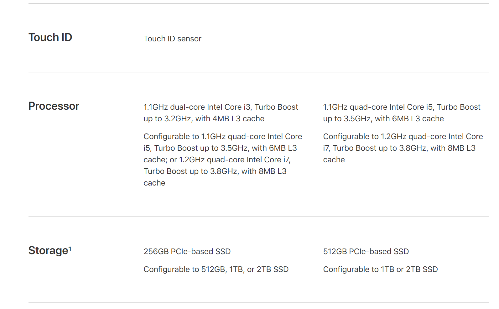
When we approached Intel asking what these CPUs were, and the official line is:
“The ‘N’ notes a slightly differentiated, customer-specific version of those SKUs. Those slight differences require a signifier for our internal SKU management and ordering systems. The N is not a new subfamily or directly connected to a specific set of features, for example.”
This goes in line with what we stated above about customer-specific binning. Apple will no doubt be ordering a few million of these CPUs, so Intel is prepared to add an extra binning step just for the business.
Related Reading- The Ice Lake Benchmark Preview: Inside Intel's 10nm
- Examining Intel's Ice Lake Processors: Taking a Bite of the Sunny Cove Microarchitecture
- Intel Begins Commercial Shipments of 10nm Ice Lake CPUs to OEMs
- Intel Unveils 10th Gen Core Ice Lake-U & Ice Lake-Y Mobile CPUs
- Intel: 28 W Ice Lake Core i7-1068G7 Coming Q1
More...
-
03-25-20, 01:43 PM #10455
Anandtech: OWC Refreshes Mercury Elite Pro DAS: Up to 16 TB over USB 3.2
OWC has announced a new version of its Mercury Elite Pro DAS, the company's entry-level external storage box. The refreshed DAS can house one 3.5-inch hard drive, allowing it to provide capacities of up to 16 TB using today's HDDs.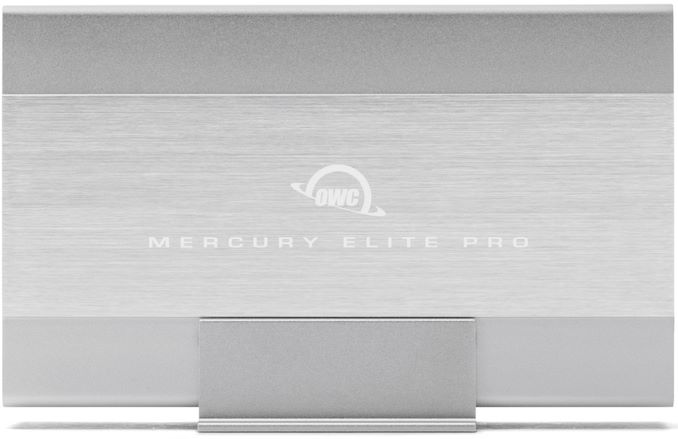
The OWC Mercury Elite Pro DAS is available in 1 TB, 2 TB, 4 TB, 6 TB, 8 TB, 12 TB, 14 TB, and 16 TB versions. The devices can be stacked, so those who need greater capacities can easily get it. All the SKUs are powered by 7200 RPM hard drives, so they offer a rather decent level of performance, up to 283 MB/s, which is good enough for music, videos, photos, and business files. Externally, the DAS has a USB 3.2 Gen 1 interface with up to 5 Gbps throughput.
The Mercury Elite Pro DAS comes in a brushed aluminum chassis with venting, so it does not rely on active cooling, making the hard drive inside the only major noise source.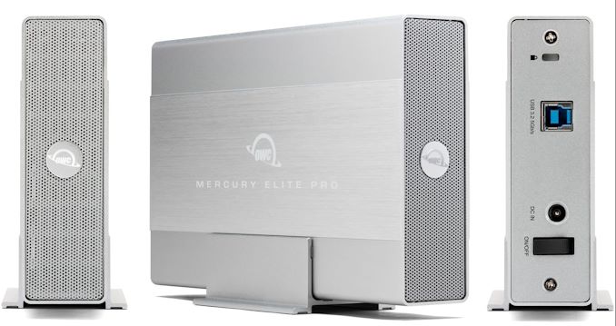
OWC’s new entry-level DAS is compatible with Apple macOS X, Microsoft Windows, Linux, Sony PlayStation 4, Xbox consoles, and Smart TVs. In addition, they are support Apple Time Machine and Windows File History backups.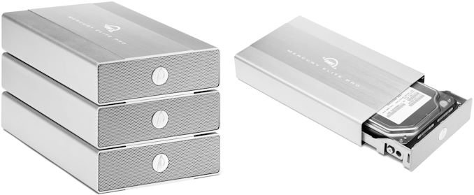
OWC has already started sales of the Mercury Elite Pro. Just the enclosure itself is priced at $49, a 2 TB SKU costs $129, whereas the top-of-the-range 16 GB module carries a $579 price tag.
Related Reading:
- OWC Launches ThunderBay 4 Mini DAS: 4 SATA Bays With SoftRAID, Up to 1.5 GB/s
- OWC Mercury Elite Pro Dock / DAS Combo: TB3, up to 28 TB, USB 3.0, DP, GbE, SD
- OWC’s Intros Thunderbolt 3 Pro Dock with 10 GbE, USB 3.0, eSATA, Card Readers & More
- OWC Unveils Second-Gen ThunderBlade External SSDs: 2800 MB/s Starting at $799
Source: OWC
More...
-
03-25-20, 08:14 PM #10456
Anandtech: GSMA Details Refund Packages for MWC20 Attendees & Exhibitors
Following the cancellation earlier this year of the 2020 Mobile World Congress trade show, GSMA, the organizer behind the even, has finally disclosed details regarding the compensation packages that it will provide to attendees and exhibitors who had already paid to attend the show. The organization will refund price of tickets to individual visitors, while exhibitors will have two options, depending on how much they've spent.
More...
-
03-26-20, 08:47 AM #10457
Anandtech: Huawei Announces P40, P40 Pro and P40 Pro+: A New Generation of Cameras
Today, Huawei is doubling down on its efforts to regain western market share, revealing brand-new hardware as well as expanding the company’s AppGallery app store, introducing the new P40, P40 Pro as well as the P40 Pro+.
The trio of phones are successors to the company’s photography-focused P series, yet again pushing the envelope in terms of innovative camera hardware, adding to the mix some new exclusive sensors, including a new large 1/1.28” 52MP RYYB unit, as well as coming with an array of various other modules – including an expansive telephoto module selection.
More...
-
03-26-20, 08:47 AM #10458
Anandtech: Folding@Home Reaches Exascale: 1,500,000,000,000,000,000 Operations Per Se
Folding@home has announced that cumulative compute performance of systems participating in the project has exceeded 1.5 ExaFLOPS, or 1,500,000,000,000,000,000 floating point operations per second. The level of performance currently available from Folding@home participants is by an order of magnitude higher than that of the world’s most powerful supercomputer.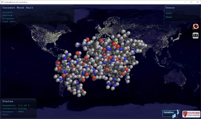
Right now, cumulative performance of active CPUs and GPUs (which have returned Work Units within the last 50 days) participating in the Folding@home project exceeds 1,5 ExaFLOPS, which is 10 times faster than performance of IBM’s Summit supercomputer benchmarked for 148.6 PetaFLOPS. To get there, Folding@Home had to employ 4.63 million CPU cores as well as nearly 430 thousand GPUs. Considering the nature of distributed computing, not all CPU cores and GPUs are online at all times, so performance available for Folding@home projects varies depending on availability of hardware.
The outbreak of COVID-19 has been taxing for a number of computational biology and chemistry projects. IBM recently formed its COVID-19 High Performance Computing Consortium that pools together major supercomputers run by various research institutions and technology companies in the USA to run research simulations in epidemiology, bioinformatics, and molecular modeling. Cumulative performance of supercomputers participating in IBM’s COVID-19 HPC Consortium is 330 PetaFLOPS.Folding@home Active CPUs & GPUs
Reported on Wed, 25 Mar 2020 23:04:31 GMTAMD GPUs NVIDIA GPUs CPUs CPU Cores TFLOPS x86 TFLOPS Windows 75,823 314,952 474,277 3,588,315 680,371 1,384,998 Linux 3,675 41,113 78,124 811,997 85,028 167,152 macOS - - 41,582 230,198 2,578 2,578 Total 79,498 356,065 593,983 4,630,510 767,977 1,554,728 Note: CPUs and GPUs which have returned Work Units within the last 50 days are considered Active.
Folding@home distributed computing project uses compute capabilities to run simulations of protein dynamics in a bid to better understand them and find cures for various diseases. Recently F@H started to run projects simulating theoretically druggable protein targets from SARS-CoV-2, which attracted a lot of attention as SARS-CoV-2 and COVID-19 are clearly the hottest topics these days.
We at AnandTech also have our Folding@Home team, which are currently in a race against our sister site Tom's Hardware. If you have a GPU spare that's not too old, think about joining us in our battle. We are Team 198.
Related Reading:
- IBM & Partners to Fight COVID-19 with Supercomputers, Forms COVID-19 HPC Consortium
- Help Fight COVID-19 and Tom's Hardware: Join The Great Folding@Home Coronavirus Race
Source: Folding@Home Twitter
More...
-
03-26-20, 02:55 PM #10459
Anandtech: Qualcomm to Update Smartphone GPU Driver Every Quarter, Develops GPU Inspe
As part of its Snapdragon Elite Gaming initiative, Qualcomm previously announced its intentions to release quarterly driver updates for its Adreno GPUs. And now at long last, the first update is set to arrive. In addition, the company has developed an Android GPU Inspector tool to help game designers to optimize their applications for better performance.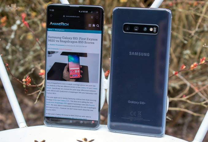
While standalone driver updates are still a new concept to smartphones, they are a tried and true aspect of PCs. As a result of being able to deliver periodic driver updates separate from the OS, PC GPU vendors have been able to boost gaming performance and fix bugs in games at a fairly rapid pace, to the benefit of PC gamers everywhere. Now, as part of their Snapdragon Elite Gaming program, Qualcomm wants to bring those same benefits to smartphones, shipping their own driver regular updates to phones so that these performance and feature updates are more readily available to smartphone gamers.
Overall, Qualcomm has stated that it wants to release new drivers for its Snapdragon SoCs every quarter for two to three years after launch. However, it should be noted that the company will not be going around handset vendors in delivering driver updates; the drivers will be sent to smartphone manufacturers, who in turn have to push them to the Google Play Store (or app stores in China). Which means that while Qualcomm hopes that their OEM partners will stick to the quarterly release schedule, it does not have control over what the OEMs ultimately do.
The first SoCs to get quarterly GPU driver are the current-generation Snapdragon 865 and Snapdragon 765/765G, as well as previous-generation Snapdragon 855. The first smartphones to be updated, in turn, will be the Samsung Galaxy S10, Samsung Galaxy Note 10, and Google’s Pixel 4 series. Meanwhile other handsets will be updated later.
In addition to drivers set to be updated quarterly, Qualcomm has also teamed up with Google to create the Android GPU Inspector tool, which promises to help discover performance optimization opportunities. According to Qualcomm, the tool helped Google and an unnamed game developer find an optimization that ‘saved the game 40% in GPU utilization’ on the Pixel 4 XL, which enabled smoother gameplay and longer battery life.
And this kind of close collaboration with game designers will not end with the Android GPU Inspector tool. Select game studios will get beta versions of Adreno GPU software driver in a bid to provide feedback to Qualcomm and, possibly, optimize their titles better.
Related Reading:
- The Snapdragon 865 Performance Preview: Setting the Stage for Flagship Android 2020
- The ASUS ROG Phone II Review: Mobile Gaming First, Phone Second
- Qualcomm Announces Snapdragon 865 and 765(G): 5G For All in 2020, All The Details
- Qualcomm to Start XR2 Reference Design Programme for AR/VR/XR
- Samsung Galaxy Book S Laptop with Snapdragon 8cx: Pre-Order at $999 from Today
Sources: Qualcomm, AndroidAuthority
More...
-
03-26-20, 02:55 PM #10460
Anandtech: Richard Yu Press Interview: Huawei's CEO on COVID-19 and Huawei Apps
Today Huawei launched its latest generation of photography focused smartphone: the P40 series. This series consists of the P40, the P40 Pro, and the P40 Pro+, starting at €799 for the cheapest going up to €1399 for the high-end model, which features a 40W wireless charge mode, a 6.58-inch OLED 90 Hz display, 10x optical zoom, up to 100x zoom, Wi-Fi 6, and a range of new photography features to get the best shot.
After the launch, Huawei’s Consumer Business Group (CBG) CEO Richard Yu invited the press to a group question and answer session. There were two main topics that dominated the session - how the prevalence of COVID-19 is affecting Huawei’s strategy, but also how the continuation of the US ban on Huawei interacting with US companies is affecting users and in particular the available apps on Huawei’s own App Gallery that can’t use Google’s services.
More...


 Quote
QuoteThread Information
Users Browsing this Thread
There are currently 7 users browsing this thread. (0 members and 7 guests)


Bookmarks