

Results 10,711 to 10,720 of 12096
Thread: Anandtech News
-
08-12-20, 03:15 AM #10711
Anandtech: US Appeals Court Reverses Antitrust Ruling in FTC vs Qualcomm
It’s been over three years since the United States FTC had charged Qualcomm with antitrust violations over cellular modem patents and business practices. That suit ultimately received a ruling in May of 2019 against Qualcomm, resulting in an injunction for Qualcomm to renegotiate its licensing agreements with its customers. Qualcomm had subsequently appealed the ruling, putting the order on hold, and today, a bit over a year later, the Ninth Circuit Court of Appeals has finally issued an opinion, reversing and vacating the injunction, resulting in a win for Qualcomm at this moment in time.
The appeals court’s opinion centres around the FTC’s use of anti-trust law to hold Qualcomm accountable for some of its controversial business practices in how it handles licensing of its patent portfolio and its “no license, no chip” mode of operation. The opinion attacks the original judgment in that the arguments presented do not fall under the umbrella of anti-trust law violations, and instead it being a matter of contract and patent law.
The original charge revolved around Qualcomm’s supposed refusal to license cellular patents to competitor chip vendors, with the company countering this accusation that its patents only apply to OEM products, not the chips of components themselves:
“Qualcomm argues that it has no antitrust duty to deal with its rivals, and in any case OEM-level licensing is consistent with Qualcomm’s SSO commitments because only OEM products (i.e., cellphones, tablets, etc.) “practice” or “implement” the standards embodied in Qualcomm’s SEPs. Furthermore, Qualcomm argues that it substantially complies with the TIA and ATIS requirements by not asserting its patents against rival chipmakers.”The appeals panel has upheld Qualcomm’s notion and point-of-view of the practice, stating that there is no antitrust law which prohibits the company from applying licensing arrangements in this way.
More precisely, the matter of Qualcomm collecting royalties from OEMs is said to be due a change in patent law, that forced the company to stop giving non-exhaustive licenses to other chip vendors:
“… Qualcomm claims that it never granted exhaustive licenses to rival chip suppliers. Instead, as the 1999 email suggests, it entered into “non-exhaustive, royalty-bearing agreements with chipmakers that explicitly did not grant rights to the chipmaker’s customers.” Appellant’s Opening Br. at 45. According to Qualcomm, it ceased this practice in response to developments in patent law’s exhaustion doctrine, see, e.g., Quanta Comput., 553 U.S. at 625 (noting that “the initial authorized sale of a patented item terminates all patent rights to that item”), which made it harder for Qualcomm to argue that it could provide “non-exhaustive” licenses in the form of royalty agreements.”Because Qualcomm applies this practice equally between all OEMs, and there is no history of the company ever granting exhaustive licenses to a chip vendor, the appeals panel also failed to determine any anticompetitive behaviour on the part of the company, calling Qualcomm’s business model “chip-supplier neutral”, and does not undermine competition in the antitrust market.
“… Qualcomm’s practice of licensing its SEPs exclusively at the OEM level does not amount to anticompetitive conduct in violation of § 2, as Qualcomm is under no antitrust duty to license rival chip suppliers.”As Qualcomm is seen as not having performed any anticompetitive behaviour in terms of its willingness to license patents to OEMs, and the fact that it gives a “CDMA ASIC” waiver license to chip vendors for free in order for them to internally exercise the technology before they sell it onto their customers, its refusal to give chip vendors non-exhaustive patent licenses is not seen as a matter of antitrust law, and the original ruling to be void in this regard.
The appeal opinion also addresses the third matter of the alleged exclusivity deal that Qualcomm had entered with Apple in 2011 and 2013, that given the effect of this deals had not stifled the competition (And arguing with the fact that Intel had subsequently won Apple contracts in following years), that it also did not go against antitrust law.
Overall, the opinion of the appeals panel today represents a major blow to the FTC and its original legal tactic and usage of antitrust law. Whilst this is a major win for the company, it’s not completely out of the woods as the company’s practises could still be in violation of contract and patent law:
“To the extent Qualcomm has breached any of its FRAND commitments, a conclusion we need not and do not reach, the remedy for such a breach lies in contract and patent law.”While currently Qualcomm can continue its business practises licensing model, it’s likely to continue to receive future scrutiny in regards to the amount of the fees it charges.
Related Reading:- United States Rules Qualcomm In Violation of Antitrust Laws - Qualcomm To Appeal
- United States FTC Charges Qualcomm with Antitrust Violations over Cellular Modem Patents & Technology
- European Union Fines Qualcomm $1.23 Billion for Anti-Competitive Apple Deal
- European Commission Fines Qualcomm €242m For Anti-trust Violations
- Taiwan Fines Qualcomm $773 Million for Antitrust Violations
- South Korea Fines Qualcomm $865 Million for Anti-Trust Violations
- China Fines Qualcomm $975 Million for Anti-trust Violations
- European Union Opens Up Antitrust Investigation Into Qualcomm
More...
-
08-12-20, 11:15 AM #10712
Anandtech: Microsoft Opens Pre-Orders for Surface Duo - US Only
Late last year in October, Microsoft had announced the Surface Duo, the company’s first ever Android device and first-party smartphone (if you can call it that) release in years. What makes the Surface Duo special is its symmetric dual-screen nature and 360° hinge mechanism that allows the device to fold itself shut like a book – to fully opening itself up with two opposing displays. Today Microsoft is finally making the Surface Duo available for pre-order – although availability will be limited to the US.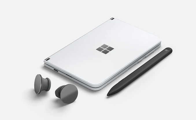
Starting off with the uninteresting stuff – the internal hardware of the Surface Duo isn’t all that exciting as it features a last generation Snapdragon 855 SoC. Given the device’s early announcement last year it seems Microsoft took a long time to bring the device to market. We’re seeing a standard amount of DRAM and storage space with 6GB and either 128GB or 256GB options. All in all there’s nothing too special about the internals here and are in line with 2019 flagships.Microsoft Surface Duo Surface Duo SoC Qualcomm Snapdragon 855
1x Kryo 485 (Cortex-A76) @ 2.84GHz
3x Kryo 485 (Cortex-A76) @ 2.42GHz
4x Kryo 485 (Cortex-A55) @ 1.80GHz
Adreno 640 @ 585MHzDRAM 6GB LPDDR4X Display Dual 5.6" solid OLED with 360° hinge
1800 x 1350 (4:3)
Unfolded 8.1" effective diagonal at 2700x1800 (3:2)Size Height 145.2 mm Width 93.3 mm (closed) - 186.9 mm (open) Depth 9.9mm (closed) - 4.8 mm (open) Weight 250 grams Battery Capacity 3577mAh total (dual cells) Wireless Charging - Rear Cameras Main 11MP 1.0 µm
f/2.0Telephoto - Wide - Extra - Front Camera - Storage 128 / 256 GB UFS 3.0 I/O USB-C Wireless (local) 802.11ac Wave 2 Wi-Fi
Bluetooth 5.0 LE + NFCCellular (Category 12/5)
DL = 1200Mbps
5x20MHz CA, 256-QAM
UL = 150Mbps
2x20MHz CA, 64-QAMOther Features It folds Dual-SIM 1x nanoSIM + eSIM Launch Price $1399
The device’s key characteristic is naturally its symmetrical folding design with two 5.6” 1800 x 1350 resolution OLED screens. Although we call this a folding device, this doesn’t actually apply to the displays as they’re two distinct units covered with solid glass.
Further unique to the design is the hinge mechanism which is symmetrical as well – it allows for a full 360° tilt of the two sides, meaning you can have the device either fully shut, or you can have it fully opened with both screen facing outwards.
Microsoft opted for relatively unusual form-factors here as the screens are each 4:3 – and when opened up it gives you a sort of effective 8.1” diagonal 3:2 surface to work with.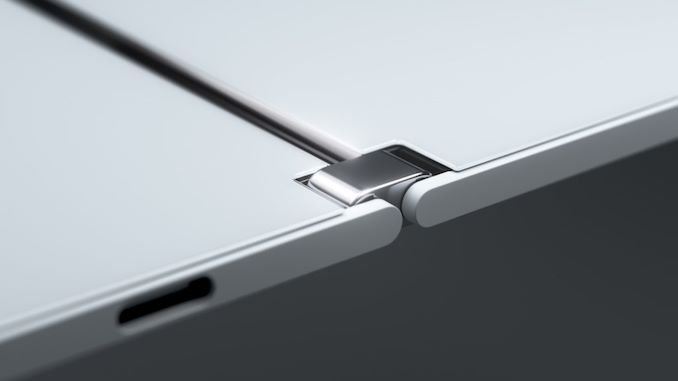
The dimensions of the device come at 145.2mm height in portrait mode, and one side is 93.3mm wide, which opens up till 186.9mm. Each half is extremely thin at only 4.8mm meaning that even when folded it remains a relatively reasonable 9.9mm in thickness.
The device’s 360° folding nature means that the internal screen surface can face completely outwards, and Microsoft took advantage of this for their camera design, of which the Surface Duo only has a single unit. The 11MP 1µm pixel f/2.0 standard wide-angle unit is relatively conservative in specifications, but that’s the compromise that had to be made to fit into a 4.8mm thick chassis and not having the possibility to employ a camera bump.
Microsoft positions the Surface Duo as a productivity device, and its first-party applications such as the Microsoft 365 suite will be optimised for the experience. This seemingly will be the deciding factor as to how the Surface Duo will be received, as it represents quite a niche device market.
The Surface Duo is available for pre-order now at a very high price of $1399, with availability only in the US and compatibility with AT&T, T-Mobile and Verizon, with availability starting September 10th.
The device’s high price and relatively lacklustre specifications will likely result in limited adoption amongst users- and the device in general feels more like an experiment than a product that’s aimed at commercial success.
Related Reading:- Microsoft Announces Surface Duo - An Android Dual-Screen Device
- Samsung Announces Galaxy Z Fold 2: Second-Generation Foldable
More...
-
08-13-20, 10:59 AM #10713
Anandtech: Intels Xe-HPG GPU Unveiled: Built for Enthusiast Gamers, Built at a Third
Among the many announcements in today’s Intel Architecture Day, Intel is also offering a major update to their GPU roadmap over the next 24 months. The Xe family, already jam-packed with Xe-LP, Xe-HP, and Xe-HPC parts, is now getting a fourth planned variant: Xe-HPG. Aimed directly at the enthusiast gamer market, this latest Xe variant will be Intel’s most gaming-focused part yet, and the biggest step yet in Intel’s plans to be more diversified in its foundry sources.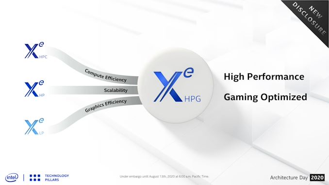
So what is Xe-HPG? At a high level, it’s meant to be the missing piece of the puzzle in Intel’s product stack, offering a high-performance gaming and graphics-focused chip. This is as opposed to Xe-HP, which is specializing in datacenter features like FP64 and multi-tile scalability, and Xe-HPC which is even more esoteric. In that respect, Xe-HPG can be thought of as everything in the Xe family, distilled down into a single design to push FLOPs, rays, pixels, and everything else a powerful video card might need.
Like with the rest of Intel’s forward-looking Xe announcements, the company isn’t offering performance projections, features, or the like. But we do have some small details on what to expect.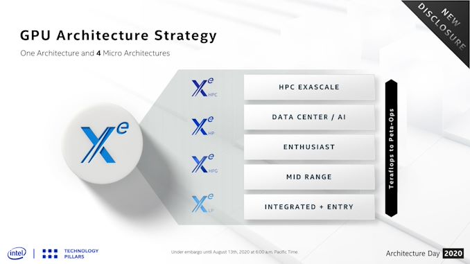
First and foremost, beyond going after the enthusiast performance space, Intel has confirmed that this part will support ray tracing. A marquee feature of high-end video cards, ray tracing will take on even greater important over the coming years as the soon-to-launch next-generation consoles head out the door with the feature as well, eventually transforming it into a baseline feature across all gaming platforms. Similarly, ray tracing is a critical component of Microsoft’s DirectX 12 Ultimate standard, which given the timing of this GPU and Intel’s intentions, I would be shocked if Intel didn’t support in full.
The chip will be built on the foundation that is Xe-LP. However it will also pull in technologies that Intel is pioneering for Xe-HP, and Xe-HPC. Not the least of which is raw scalability, which is being able to take the Xe-LP foundation and scale it up to hundreds (if not thousands) of GPU execution units. But Intel is also pulling what they are calling “compute frequency enhancements” from Xe-HPC, which presumably will allow them to maximize the chip’s overall clockspeeds. All told, I won’t be too surprised if it looks a lot like Xe-HP in general, except with server-driven features like fast FP64 support and multi-tiling stripped out.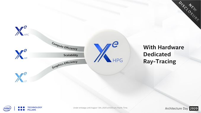
But Xe-HPG will also bring something new to the table for the entire Xe family: GDDR6 support. Intel is confirming that the chip – or rather, the microarchitecture the chip will be based on – will be designed to work with GDRR6. This is as opposed to Xe-HP(C), which as high-end server parts use HBM, and Xe-LP, which is designed for use with more conventional memory types. GDDR6 compatibility is a unique need that reflects this is a gaming focused part: GDDR6 provides the memory bandwidth needed for high-performance graphics, but without the stratospheric costs of HBM memory (a problem that has impacted some other high-end GPUs over the years). In a further twist, Intel apparently licensed the GDDR controller IP from outside the company, rather than developing it in-house; so Xe-HPG will have a very notable bit of external IP in it.
But perhaps most interesting of all for graphics insiders and Intel investors alike is where Xe-HPG will be built: not at Intel. As part of their Architecture Day roadmap, Intel has confirmed that the part will be made at an external fab. In fact it’s the only Xe part where the GPU (or at least the compute element) is being made entirely at a third-party fab. Intel of course will not reveal which fab this is – if it’s TSMC or Samsung – but it means we’re going to see a complete Intel GPU built at another fab. If nothing else, this is going to make comparing Xe-HPG to its AMD and NVIDIA rivals a lot easier, since Intel will be using the same fab resources.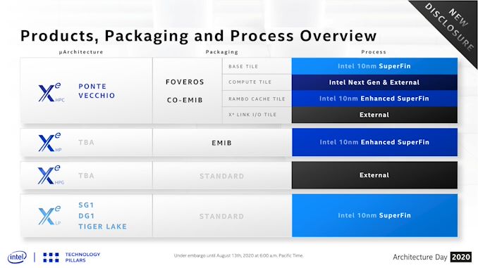
Looking at the same roadmap, it’s worth pointing out that Intel won’t be using any of their advanced packaging technologies for the part. Since they’re not using HBM and they’re not doing multi-tiling, there’s no need for things like EMIB, never mind Foveros. There’s still a lot of unknowns with the cost aspects of Intel’s advanced packaging technologies, so keeping it out of Xe-HPG will presumably help keep costs in check in a very competitive marketplace.
And that is the scoop on Xe-HPG. The latest and most gaming-focused member of Intel’s Xe GPU product stack is set to launch in 2021 – and as Intel looks to break into the wider GPU market, I don’t doubt for a second that this won’t be the last we’ll hear of it between then and now.
More...
-
08-13-20, 10:59 AM #10714
Anandtech: Intel Previews 4-Layer 3D XPoint Memory For Second-Generation Optane SSDs
As part of Intel's Architecture Day 2020 presentations, Raja Koduri spent a bit of time talking about the status of their Optane products. Most of it was a recapitulation of details Intel has previously shared. The two important Optane product updates planned for this year are the Barlow Pass second-generation Optane DC Persistent Memory Modules (DCPMM) and the Alder Stream second-generation Optane NVMe SSDs.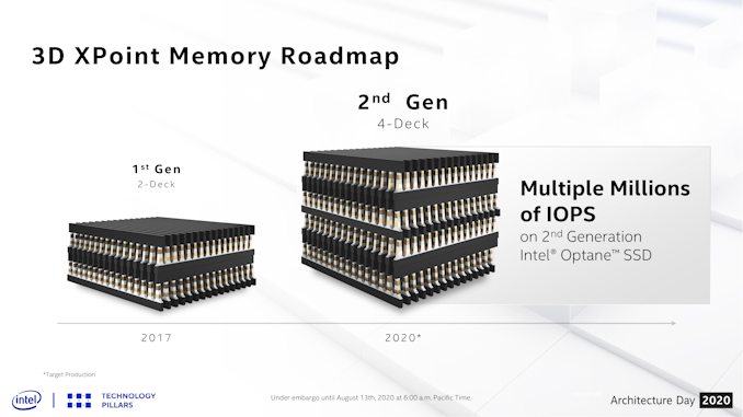
Intel has been teasing their Alder Stream second-generation Optane SSDs since last fall, with promises of off-the-charts performance increases. They've confirmed that Alder Stream will be using second-generation 3D XPoint memory, which moves from two to four layers ("decks" in Intel's slides), making this the first test of the vertical scaling potential of 3D XPoint technology. This combined with with a new SSD controller supporting PCIe 4.0 will enable "multiple millions" of IOPS, more than doubling the throughput of current Optane SSDs. Raja also mentioned that they've made optimizations to single-sector reads, so 4kB QD1 random read latency should be improved a bit as well—but this latency is already substantially limited by the latency of PCIe and NVMe command processing.
Intel recently stated that they have not yet decided where to spun up their own volume manufacturing of 3D XPoint memory, so the second-gen 3D XPoint used in Alder Stream will still be manufactured by former partner Micron and purchased by Intel.
Barlow Pass has already launched alongside Cooper Lake Xeons and will be the Optane DCPMM product for Ice Lake Xeons as well. Intel claims an average of 25% higher bandwidth for Barlow Pass than the initial Apache Pass modules for Cascade Lake Xeons.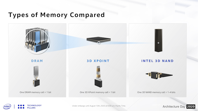 DRAM, 3D XPoint and 3D NAND memories, approximately to scale
The fine print in Intel's slides indicates that the 4-deck 3D XPoint memory used in Alder Stream Optane SSDs is not yet in mass production. That and the omission of any mention of the second-generation, 4-deck 3D XPoint memory in the context of Optane DCPMM products all but confirms that Barlow Pass is still using first-gen 3D XPoint memory. This is consistent with the more modest 25% bandwidth increase as compared to the drastic improvements due to arrive with the Alder Stream SSDs. It appears that Ice Lake servers will be getting more advanced Optane SSDs than Optane DCPMM modules, as the next generation of Optane DCPMM isn't due until the launch of Sapphire Rapids processors and the switch to DDR5.
Related Reading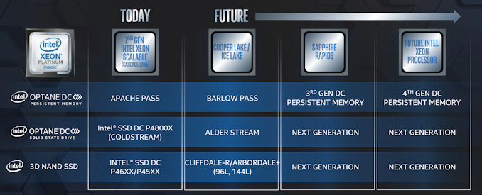
- Intel Launches Cooper Lake: 3rd Generation Xeon Scalable for 4P/8P Servers
- Intel Announces D7-P5500 and D7-P5600 Series PCIe 4.0 Enterprise SSDs
- Kioxia Releases First PCIe 4.0 SSDs: CD6 & CM6
- Intel Shares New Optane And 3D NAND Roadmap - Barlow Pass DIMMs & 144L QLC NAND in 2020
More...
-
08-13-20, 04:19 PM #10715
Anandtech: Intel Xe-HPC GPU Status Update: 4 Process Nodes Make 1 Chip
Continuing today’s GPU news from Intel’s Architecture Day presentation, on top of the Xe-LP architecture briefing and Xe-HPG reveal, the company has also offered a brief roadmap update for their flagship sever-level part, Xe-HPC.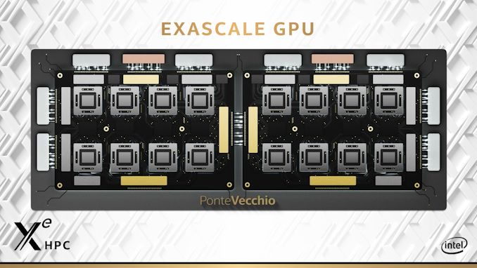
Better known by its codename of Ponte Vecchio, much to do has been made about Xe-HPC. The most complex of the Xe parts planned, it is also the cornerstone of the Intel-powered Aurora supercomputer. Xe-HPC is pulling out all of the stops for performance, and to get there Intel is employing every trick in the book, including their new-generation advanced packaging technologies.
The big revelation here is that we finally have some more concrete insight into what manufacturing processes the various tiles will use. The base tile of the GPU will be on Intel’s new 10nm SuperFin process, and the Rambo Cache will be a generation newer still, using Intel’s future 10nm Enhanced SuperFin process. Meanwhile it’s now confirmed that the Xe Link I/O tile, which will be used as part of Intel’s fabric to link together multiple Xe-HPC GPUs, will be built by an external fab.
That leaves the matter of the compute tile, the most performance-critical of the GPU’s parts. With Intel’s 7nm process delayed by at least six months, the company has previously disclosed that they were going to take a “pragmatic” approach and potentially use third-party fabs. And as of their Architecture Day update, they still seem to be undecided about – or at least unwilling to disclose – just what they plan on doing. Instead, the compute die is labeled as “Intel Next Gen & External”.
It's an unusual disclosure, to say the least, as we'd otherwise expect the compute die to be made on a single process. But with no further commentary from Intel offered, make of that what you will. Perhaps they’re being straightforward, and they will actually use two very different process nodes for the compute die?
More...
-
08-14-20, 10:38 AM #10716
Anandtech: Micron Spills on GDDR6X: PAM4 Signaling For Higher Rates, Coming to NVIDIA
It would seem that Micron this morning has accidentally spilled the beans on the future of graphics card memory technologies – and outed one of NVIDIA’s next-generation RTX video cards in the process. In a technical brief that was posted to their website, dubbed “The Demand for Ultra-Bandwidth Solutions”, Micron detailed their portfolio of high-bandwidth memory technologies and the market needs for them. Included in this brief was information on the previously-unannounced GDDR6X memory technology, as well as some information on what seems to be the first card to use it, NVIDIA’s GeForce RTX 3090.
The key innovation for GDDR6X appears to be that Micron is moving from using POD135 coding on the memory bus – a binary (two state) coding format – to four state coding in the form of Pulse-Amplitude Modulation 4 (PAM4). In short, Micron would be doubling the number of signal states in the GDDR6X memory bus, allowing it to transmit twice as much data per clock.
More...
-
08-14-20, 10:38 AM #10717
Anandtech: MMD and Phillips Launch the 279C9 27" Montior: FreeSync 4K IPS & USB Type-
This week MMD and Phillips have unveiled its latest display in their ever-growing product range, the Phillips 279C9. A 27-inch monitor aimed squarely at content creators and professionals, the 279C9 is based around a 3840 x 2160 60 Hz IPS display and includes features such as a five-port USB hub (including a USB Type-C port), as well as DisplayHDR 400 certification.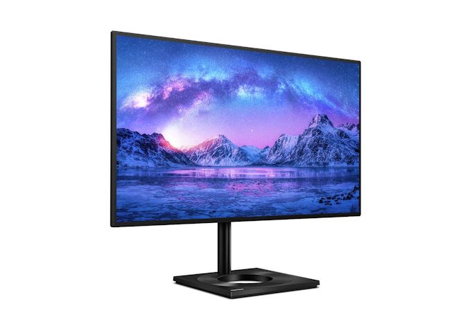
Digging into the monitor's specifications, as is typical with most content-focused monitors in this range, Phillips' 279C9 has clearly been tuned for its target market. The 3840x2160, 16:9 aspect ratio panel is a very straightforward choice, with MMD tapping an IPS panel for viewing angles and color stability. As this isn't a gaming-focused display, the monitor tops out at a 60Hz refresh rate, though there is official support for VESA Adaptive Sync to offer variable refresh support and the monitor carries AMD's FreeSync branding.
Otherwise the 279C9 has a typical static contrast ratio of 1300:1, with "Mega Infinity DCR" smart contrast technology. Meanwhile the monitor is DisplayHDR 400 certified, meaning it can offer 400 nits maximum brightness in HDR mode, and Phillips lists 400 nits as the average brightness as well. The display is framed by a fairly skinny bezel with a 596.74 x 335.66 mm (H x V) viewing area, and the screen itself is coated with an anti-glare 3H coating.
Meanwhile there is an interesting array of input and output options, including a USB Type-C input, which along with DP alt mode input allows for fast data transfer and official charging support for devices such as laptops. This is joined by dual HDMI 2.0 inputs, as well as a single DisplayPort 1.4 output. As for downstream connectivity, it also includes four USB 3.2 Type-A ports, and while Phillips doesn't distinguish between the use of USB 3.2 G2 or G1 connectivity, it is likely the latter. Two of the Type-A ports also feature USB fast charging support. Finally, the monitor includes is a pair of 2 W speakers.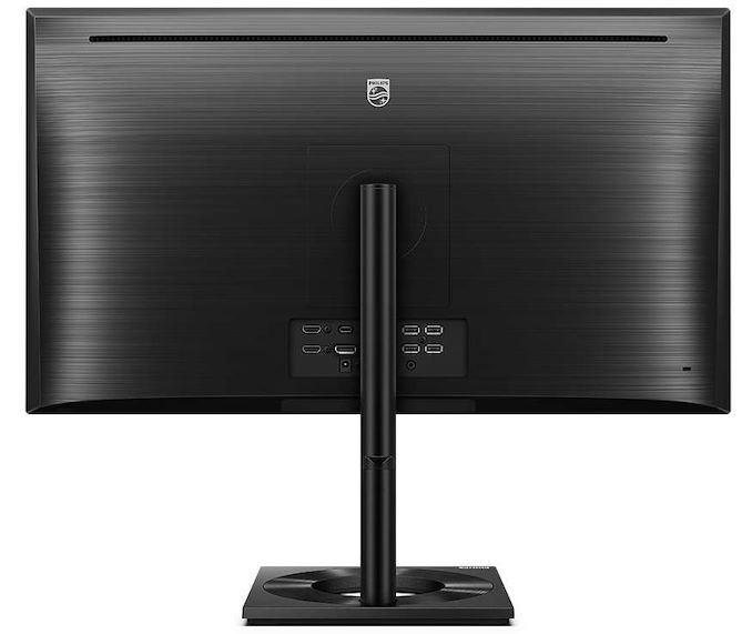
In terms of availability, Phillips plans to launch the 27" 279C9 4K display at the end of August, with an MSRP of £449. At present, Phillips hasn't announced its US pricing or availability outside of the UK market.Phillips 279C9 27" Monitor Specifications Panel 27" IPS Native Resolution 3840 x 2160 (16:9) Maximum Refresh Rate 60 Hz Response Time 5 ms (grey to grey) Contrast 1300:1 (Mega Infinity DCR) Backlight Type W-LED Viewing Angles 178°/178° Horizontal/Vertical Aspect Ratio 16:9 Color Gamut NTSC 90.7%
sRGB 109%DisplayHDR Tier DisplayHDR 400 Inputs 1 x DisplayPort 1.4
2 x HDMI 2.0
1 x USB Type-C (video/data) - 65 W charging
4 x USB Type-A
1 x 3.55 mm headphone outAudio Dual 2 W Speakers MSRP (GBP) £449
Gallery: Phillips 279C9 Gallery


Related Reading- AOC Announces New AGON Gaming Monitors, 24" 240Hz TN, 27" 165Hz NanoIPS
- Xiaomi Releases 34" WQHD 144Hz Curved Gaming Monitor for 399€
- ViewSonic Announces Elite XG270QC Monitor: 1440@165Hz, Curved For Gaming
- DisplayPort Alt Mode 2.0 Spec Released: Defining Alt Mode for USB4
More...
-
08-14-20, 06:17 PM #10718
Anandtech: Intel Brand Tie-ins: New Avengers Packaging Gives You a New Box To Play Wi
When buying a new processor, what’s the first thing to look for? Price? Performance? Frames per Second? The Box? Intel’s new brand tie-in with Marvel’s Avengers now seems official, according to the @IntelGraphics twitter handle. With the new special edition processors, users can look forward to a brightly painted box. Yes, that’s pretty much it. Oooh, shiny shiny.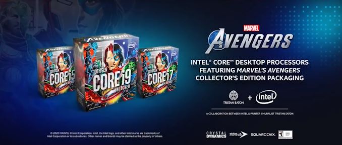
Leaks have suggested that these new boxed processors will carry new versions of Intel’s overclockable Comet Lake processors, such as the Core i9-10900K which will become new Core i9-10900KA models in Intel's database, however we are waiting on confirmation from Intel.
If this ends up being a success for Intel, no doubt it will set a precedent for future processor tie-ins. It is unclear if this arrangement involves Intel licensing the Marvel brand, or Marvel is paying Intel for co-branding ahead of Marvel's new videogame, the Marvel Avengers, set to launch on September 4th for Xbox, Playstation, and PC. There have also been suggestions that these processors may also carry codes to download extras for the game, perhaps skins or such, but again this has not been confirmed, nor is it clear that the game has any special Intel-specific acceleration for better gameplay. Imagine if the game detects the CPU string as '10900KA' and offers different abilites or modes - that would certainly interesting as to the mods that would appear to get around that restriction.
Pricing and availability are currently unknown, although we're expecting more details come September 4th.
Source: Intel Gaming on Twitter
Gallery: Intel Brand Tie-ins: New Avengers Packaging Gives You a New Box To Play With

More...
-
08-14-20, 06:17 PM #10719
Anandtech: Intel Next-Gen 10-micron Stacking: Going 3D Beyond Foveros
One of the issues facing next-generation 3D stacking of chips is how to increase the density of the die-to-die interface. More connections means better data throughput, reducing latency and increasing bandwidth between two active areas of silicon that might be manufactured at different process nodes. There’s also a consideration for power and thermal hotspots as well. Intel has been developing its own physical interconnect topologies, most of which we’ve covered in detail before, such as the Embedded Multi-Die Interconnect Bridge (EMIB) that allows 2D expansion and Foveros die-to-die 3D staking that enables vertical expansion. As part of Intel’s Architecture Day 2020, we have a glimpse into Intel’s future with hybrid bonding._575px.jpg)
There are several holistic metrics to measure how ‘good’ an interconnect can be; the two that are easiest to understand are density of connections (bump density) and energy (how much energy it takes to transfer a bit).
Intel’s own slides show us that EMIB’s bump density is good for ~400 per square millimeter, with a power of 0.50 picojoules per bit transferred. Foveros takes that a step further, supporting 400-1600 bumps per square millimeter, and an average power of 0.15 picojoules per bit transferred.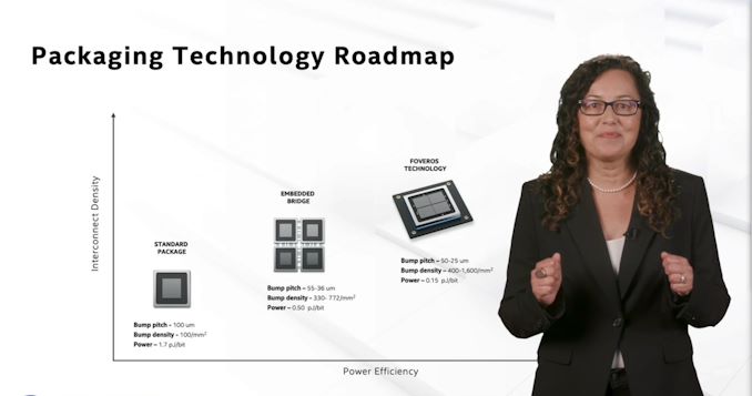
Intel's Ramune Nagisetty showcasing current packaging technologies at Intel
The next era of ‘Hybrid Bonding’ that Intel is going towards improves both metrics by around a factor of 3-10. The new test chips that Intel has just got back into the lab, involving stacked SRAM, goes towards the 10000 bumps per square millimeter range, with a power under 0.05 picojoules per bit. According to Intel this allows for smaller and simpler circuits, with lower capacitance and better efficiency. Nothing to be said about yields however!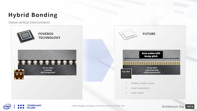
With these new bonding and stacking technologies, the question always becomes one of thermals, and how Intel might stack two performance-related bits of silicon together. In the discussions as part of Architecture Day, Intel stated that these stacked designs require having all layers designed together, rather than independently, in order to manage the electrical and thermal characteristics. As far as Intel sees it, the most power hungry layer is required to go on the top of the stack for the time being, which obviously means that the power connections have to either rise up through the lower layers, or there has to be some form of cantilevered situation where power connections can happen off the edge of the bonding – Intel calls this technology ODI, to support different sized silicon layers.
With the future of high performance and high efficiency computing coming to a head with new packaging technologies, finding the right way of going forward is ever critical. For a context on timeline, Intel’s Ramune Nagisetty has stated that Foveros was patented back in 2008, but it took nearly a decade for the process to become physically viable at scale and high-enough yielding for a product to come to market.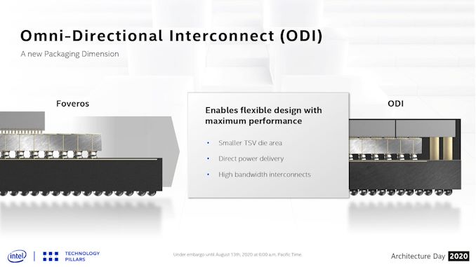
Related Reading- An Interconnected Interview with Intel’s Ramune Nagisetty: A Future with Foveros
- Intel: Lakefield in 2020, Possible 5G on Foveros
- Intel’s Xe for HPC: Ponte Vecchio with Chiplets, EMIB, and Foveros on 7nm, Coming 2021
- Hot Chips 31 Live Blogs: Intel Lakefield and Foveros
- Intel's Interconnected Future: Combining Chiplets, EMIB, and Foveros
- The Intel Lakefield Deep Dive: Everything To Know About the First x86 Hybrid CPU
Gallery: Intel Next-Gen 10-micron Stacking: Going 3D Beyond Foveros
_thumb.jpg)
_575px_thumb.jpg)
_carousel_thumb.jpg)
_carousel_thumb.jpg)
_thumb.jpg)
More...
-
08-17-20, 01:11 PM #10720
Anandtech: Hot Chips 2020 Live Blog: IBM z15, a 5.2 GHz Mainframe CPU (11:00am PT)
Hot Chips has gone virtual this year! Lots of talks on lots of products, including Tiger Lake, Xe, POWER10, Xbox Series X, TPUv3, and a special Raja Koduri Keynote. Stay tuned at AnandTech for our live blogs as we commentate on each talk.
More...


 Quote
QuoteThread Information
Users Browsing this Thread
There are currently 14 users browsing this thread. (0 members and 14 guests)


Bookmarks