

Results 10,731 to 10,740 of 12096
Thread: Anandtech News
-
08-20-20, 02:19 PM #10731
Anandtech: Western Digital's USB 3.1 Gen 2 WD My Passport SSD Gets an NVMe Refresh
Western Digital's lineup of direct-attached storage (DAS) products targets a range of markets and form-factors. After the acquisition of HGST / G-Technology and SanDisk, the company now offers similar products under multiple brand names. Portable bus-powered SSDs are an example. Subtle differences in the feature sets of the products enhance their appeal to the brand's target market.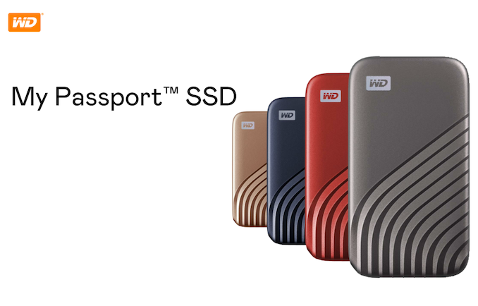
Late last year, the WD_Black P50 was introduced as the fastest non-Thunderbolt portable SSD in the market, thanks to its USB 3.2 Gen 2x2 interface. The branding clearly indicated that gamers were the target market. The regular WD branding is reserved for the My Passport series. We reviewed the first model in the My Passport SSD series back in 2017. It used the planar TLC-based SanDisk X400 M.2 SATA SSD internally with a USB 3.1 Gen 2 Type-C host interface. A new version of the My Passport SSD was released the following year with a WD Blue 3D NAND SATA SSD using 64L 3D TLC flash. Both products were held back performance-wise by the use of a SATA SSD. Today's product launch brings NVMe into the picture for the My Passport SSD product line.
The WD My Passport SSD targets productivity use-cases for business professionals (including certain content creators). The new version's industrial design and appearance has changed, with the sharp corners and fully-plastic enclosure now replaced by an aesthetically-pleasing partial metal enclosure having rounded corners. WD claims that the new design feels less rigid and more portable, and has a more pocketable shape overall.
While the WD_Black P50 and the SanDisk Extreme Pro portable SSDs meant for huge games and large media files used the WD Black SN750 NVMe SSD internally, the new WD My Passport uses the DRAM-less WD Blue SN550 NVMe SSD. This still uses a PCIe 3.0 x4 interface, and the performance numbers for the 500GB+ models are good enough to saturate a USB 3.1 Gen 2 interface. Hardware encryption is one of the key features of the higher-end products in the My Passport line-up, and the new My Passport SSD also supports AES-256 for data protection without performance loss.
The WD My Passport SSD 2020 provides a huge leap in performance (up to 1050 MBps) compared to the 2018 version (540 MBps). The 256GB capacity SKU has been phased out, and only three capacities are going to be offered - 500GB ($120), 1TB ($200 - WD's MSRP is $190), and 2TB ($380). While the My Passport SSD 2018 was available only in a single color (gray/black), the 2020 version is available in four colors - gray, red, blue, and gold.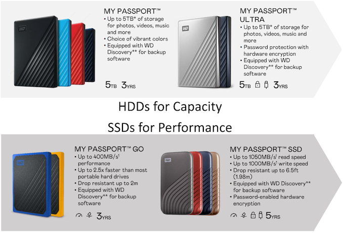
The SanDisk Extreme Pro Portable SSD is our current favorite when it comes to USB 3.1 Gen 2 portable SSDs, thanks to its compact design, performance consistency, and thermal performance. Power consumption (particularly at idle) was one of its Achilles heels compared to the OWC Envoy Pro EX USB-C (which provided similar performance, albeit in a slightly larger form-factor). If the WD My Passport SSD manages to reach close to the SanDisk Extreme Pro's performance profile while also optimizing power consumption, Western Digital may end up with yet another compelling offering in the portable SSD market.
Gallery: Western Digital's USB 3.1 Gen 2 WD My Passport SSD Gets an NVMe Refresh

More...
-
08-21-20, 11:00 AM #10732
Anandtech: Intel Xe-HP Graphics: Early Samples Offer 42+ TFLOPs of FP32 Performance
One of the promises that Intel has made with its new Xe GPU family is that in its various forms it will cater to uses ranging from integrated graphics all the way up to the high performance compute models needed for super-dense supercomputers. This means support for the types of calculations involved in simple graphics, complex graphics, ray tracing, AI inference, AI training, and the compute that goes into molecular modelling, oil-and-gas, nuclear reactors, rockets, nuclear rockets, and all the other big questions where more compute offers more capabilities. Sitting near the top of Intel’s offerings is the Xe-HP architecture, designed to offer high performance GPUs for standard server and enterprise deployments.
More...
-
08-21-20, 11:00 AM #10733
Anandtech: Intels SG1 is 4x DG1: Xe-LP Graphics for Server Video Acceleration and St
For the last few years, Intel has had a product line known as the Visual Computing Accelerator (VCA). With the VCA2 product being put on EOL earlier this year, without a replacement, we wondered where this market of Intel’s was going to go. At Intel’s Architecture Day 2020, it would appear the company is set to product a new SG1 graphics card for the server market for this purpose._575px.jpg)
Intel’s Visual Compute Accelerator
Two versions of the VCA have existed, and the hardware underneath was relatively unorthodox – Intel put three of its Xeon E3 processors onto a single PCB behind a PCIe switch.
Each processor connected to its own DRAM and chipset as well, and the goal was to use the Intel Gen graphics on-board to be able to accelerate streaming video either for consumption or gaming. These processors had the best version of Intel’s Iris Pro P6300/P580 GT4e graphics, along with 128 MB of L4 eDRAM and 32 GB of DRAM each – we saw a company that built VCE cards for Intel’s partners back at Supercomputing 2019.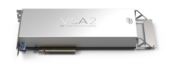
Each VCA2 was capable of transcoding 44 streams of 1080p30 H.264 simultaneously, or 14 streams of 4K30 H.264. However, the second generation VCA2 was put on the EOL path earlier this year, with no replacement in sight.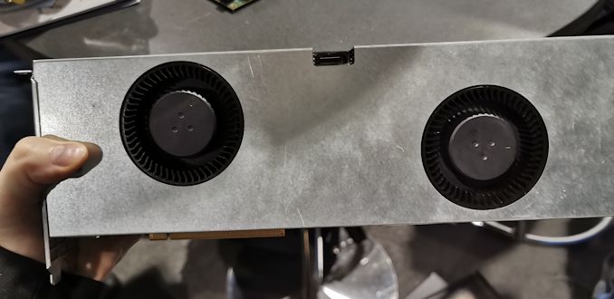
Mockup of a VCA2 with active cooling, minus aesthetics
DG1 and SG1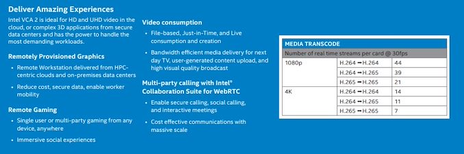
Intel declared during Architecture Day that it is planning three products built on its new Xe-LP graphics architecture. The company went into some detail about the form of Xe-LP graphics that will be going into the new Tiger Lake notebook processor, which will be the first version on the market (the full announcement of Tiger Lake is expected to be on September 2nd).
The other product previously announced on Xe-LP was DG1: Discrete Graphics 1. This is expected to be the first discrete PCIe add-in card for LP, targeting at the low-end market. Intel has already shown the software development vehicle for DG1 at CES in January 2020, with the announcement that they were starting to sample a version of the card to its software partners in advance of a bigger launch later in the year. The card was the same size of the low-to-mid range graphics on the market today, without a PCIe connector, indicating that it should be under 75W.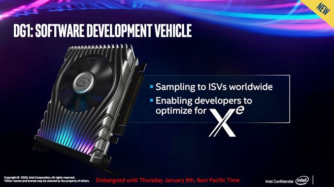
The third product is SG1: Server Graphics. Intel gave near zero details as to the setup of SG1, however they did mention that the target market was for video acceleration and streaming, exactly where the VCA series has sat. This would make it align with the mothballing of the current VCA series later this year. The VCA2 card was a GPU that had an 8-pin and a 6-pin power connector and 3x 45W CPUs as well as dual Ethernet outputs, so we fully expect SG1 to be of a similar size.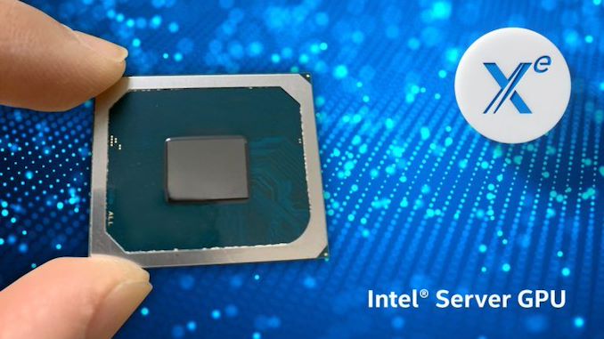
Intel's DG1, Four of which make SG1
Intel confirmed to us that SG1 will be a product containing four DG1 silicon dies, put on the same PCB. We expect there to be additional direct external networking connectivity and memory support, and it will be interesting to see how the PCIe lanes are distributed and configuration will be. Intel has confirmed that the new GPU supports AVC, HEVC, MPEG2, VP9 encode/decode and AV1 decode.
Related Reading- Intel Initiates EOL for the VCA2: Three Xeons on a PCIe Card
- Intel Announces Xeon E3-1500 v5: Iris Pro and eDRAM for Streaming Video
- The Intel Xe-LP GPU Architecture Deep Dive: Building Up The Next Generation
- Seeing Is Believing: Intel Teases DG1 Discrete Xe GPU With Laptop & Desktop Dev Cards At CES 2020
- Raja Koduri at Intel HPC Devcon Keynote Live Blog (4pm MT, 11pm UTC)
More...
-
08-21-20, 05:56 PM #10734
Anandtech: Intel Moving to Chiplets: Client 2.0 for 7nm
One of the more esoteric elements of Intel’s Architecture Day 2020 came very near the end, where Intel spent a few minutes discussing what it believes is the future of some of its products. Brijesh Tripathi, VP and CTO of Intel’s Client Computing group, laid out a vision about the future of its client products in the 2024+ future timeframe. Centered around Intel’s 7+ manufacturing process, the goal was to enable ‘Client 2.0’ – a new way to deliver and enable immersive experiences through a more optimized silicon development strategy.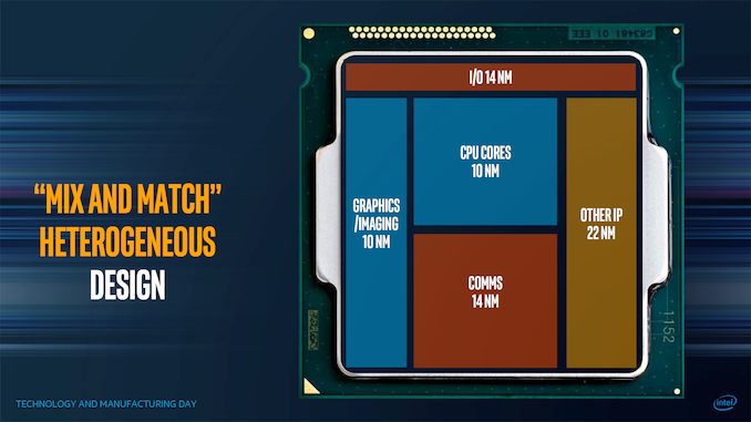
More...
-
08-21-20, 05:56 PM #10735
Anandtech: ASRock B550 Taichi Review: The $300 B550 Motherboard with Chutzpah
Outside of its Aqua series of motherboards, which come with exquisitely crafted monoblocks, ASRock's Taichi brand has been a critical part of the company's offerings in the land of premium motherboards. The ASRock B550 Taichi sits at the top of its product stack and features an impressive quality feature set. Some of the most notable features include a large 16-phase power delivery, eight SATA ports, dual M.2 slots, an Intel 2.5 GbE Ethernet controller, and an Intel Wi-Fi 6 interface. At $300 it comes equal in price with the X570 version, which leaves questions on the table as to which one is actually worth the money.
More...
-
08-22-20, 02:55 AM #10736
Re: Anandtech: Intels SG1 is 4x DG1: Xe-LP Graphics for Server Video Acceleration an
wow thanks Intel's graphics are pretty cool. However, I'll stick with playing mobile games especially modded dragon city that you can also check out from here!
Last edited by trappinggeology; 09-05-20 at 06:09 AM.
-
08-24-20, 05:56 PM #10737
Anandtech: TSMC Details 3nm Process Technology: Full Node Scaling for 2H22 Volume Pro
At TSMC’s annual Technology Symposium, the Taiwanese semiconductor manufacturer detailed characteristics of its future 3nm process node as well as laying out a roadmap for 5nm successors in the form of N5P and N4 process nodes.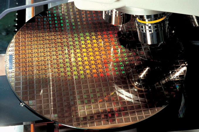
Starting off with TSMC’s upcoming N5 process node which represents its 2nd generation deep-ultraviolet (DUV) and extreme-ultraviolet (EUV) process node after the rarely used N7+ node (Used by the Kirin 990 SoC for example). TSMC has been in mass production for several months now as we’re expecting silicon shipping to customers at this moment with consumer products shipping this year – Apple’s next-generation SoCs being the likely first candidates for the node.
TSMC details that N5 currently is progressing with defect densities one quarter ahead of N7, with the new node having better yields at the time of mass production than both their predecessor major nodes N7 and N10, with a projected defect density that’s supposed to continue to improve past the historic trends of the last two generations.
The foundry is preparing a new N5P node that’s based on the current N5 process that extends its performance and power efficiency with a 5% speed gain and a 10% power reduction.
Beyond N5P, TSMC is also introducing the N4 node that represents a further evolution from the N5 process, employing further EUV layers to reduce masks, with minimal migration work required by chip designers. We’ll be seeing N4 risk production start in 4Q21 for volume production later in 2022.
Today’s biggest news was TSMC’s disclosure on their next big leap past the N5 process node generation family, which is the 3nm N3 node. We’ve heard that TSMC had been working on defining the node back last year with progress going well.
Contrary to Samsung’s 3nm process node which makes use of GAA (Gate-all-around) transistor structures, TSMC will instead be sticking with FinFET transistors and relying on “innovative features” to enable them to achieve the full-node scaling that N3 promises to bring.
Compared to it’s N5 node, N3 promises to improve performance by 10-15% at the same power levels, or reduce power by 25-30% at the same transistor speeds. Furthermore, TSMC promises a logic area density improvement of 1.7x, meaning that we’ll see a 0.58x scaling factor between N5 and N3 logic. This aggressive shrink doesn’t directly translate to all structures, as SRAM density is disclosed at only getting a 20% improvement which would mean a 0.8x scaling factor, and analog structures scaling even worse at 1.1x the density.Advertised PPA Improvements of New Process Technologies
Data announced during conference calls, events, press briefings and press releasesTSMC N7
vs
16FF+N7
vs
N10N7P
vs
N7N7+
vs
N7N5
vs
N7N5P
vs
N5N3
vs
N5Power -60% 37%
-
~17%0.55x
-45%
(1.8x)
-0.58x
-42%
(1.7x)Volume
ManufacturingQ2 2019 Q2 2020 2021 H2 2022
Modern chip designs are very SRAM-heavy with a rule-of-thumb ratio of 70/30 SRAM to logic ratio, so on a chip level the expected die shrink would only be ~26% or less.
N3 is planned to enter risk production in 2021 and enter volume production in 2H22. TSMC’s disclosed process characteristics on N3 would track closely with Samsung’s disclosures on 3GAE in terms of power and performance, but would lead more considerably in terms of density.
We’ll be posting more detailed content from TSMC’s Technology Symposium in due course, so please stay tuned for more information and updates.
Related Reading:- TSMC: N7+ EUV Process Technology in High Volume, 6nm (N6) Coming Soon
- TSMC Announces Performance-Enhanced 7nm & 5nm Process Technologies
- TSMC: Most 7nm Clients Will Transition to 6nm
- TSMC Reveals 6 nm Process Technology: 7 nm with Higher Transistor Density
- TSMC’s 5nm EUV Making Progress: PDK, DRM, EDA Tools, 3rd Party IP Ready
- TSMC: 7nm Now Biggest Share of Revenue
- TSMC: First 7nm EUV Chips Taped Out, 5nm Risk Production in Q2 2019
- TSMC Details 5 nm Process Tech: Aggressive Scaling, But Thin Power and Performance Gains
More...
-
08-25-20, 11:41 AM #10738
Anandtech: be quiet! Announces Dark Power Pro 12 PSUs: 80Plus Titanium, Up to 1500W
The increasingly popular German hardware manufacturer be quiet! has announced its latest series in its ever-growing power supply line-up, the Dark Power Pro 12. Equipped with fully digital hardware and 80 PLUS Titanium certification, the be quiet! Dark Power Pro 12 power supplies will be available in capacities of 1200 and 1500 W with the ability to combine its multiple rails into one rail for overclocked processors and graphics cards.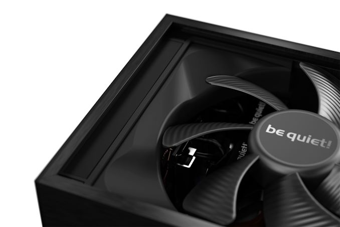
According to be quiet!, the new Dark Power Pro 12 power supplies provide efficiency of up to 94.9%, which falls into the 80 PLUS Titanium certification range, with a fully digital design including the full bridge, LLC, SR, and DC/DC componentry. The Dark Power Pro 12 series builds upon the success of its previous 11 series with the use of its overclocking key, which combines the units six multiple rails into one rail for better stability when overclocking.
The be quiet! Dark Power Pro 12 series is using a full mesh PSU front for optimal airflow, with a 135 mm Silent Wings cooling fan designed to keep it cooled efficiently, but with less noise with a maximum dBA of 31.5 at 100% load for the 1500 W model, and just 25.8 dBA for the 1200 W model under the same conditions. Both the 1500 W and 1200 W models are the same size, with dimensions of 200 x 150 x 86 mm (L x W x H), and both share a fully-modular design with seventeen cables supplied with both units. All of be quiet!'s Dark Power Pro 12 power supplies come with a 10-year manufacturer's warranty.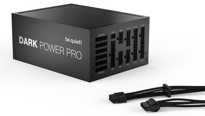
The Dark Power Pro 12 series will be available to purchase from the 8th September, with an MSRP of $449/£420/€439 for the 1500 W model, and $399/$370/€389 for the 1200 W variant.
Gallery: be quiet Unveils Dark Power Pro 12 Power Supplies, Up to 1500W, Titanium Power


Related Reading- The NZXT C650 650W PSU Review: Designed To Last
- The 1STPlayer Steampunk 80+ Gold 750W PSU Review: A New Challenger Emerges
- EVGA Launches B5 Modular PSUs: 80Plus Bronze At Up to 850 W
- NZXT Releases C-Series PSUs: 80Plus Gold and up to 850W, Built By Seasonic
More...
-
08-25-20, 11:41 AM #10739
Anandtech: TSMC Updates on Node Availability Beyond Logic: Analog, HV, Sensors, RF
Most of the time when we speak about semiconductor processes, we are focused on the leading edge of what is possible. Almost exclusively that leading edge is designed for logic circuitry where performance and power efficiency are key drivers of pushing the boundaries, but also there’s a strong market in it. Other markets use semiconductor technology where there are other factors to consider: power, analog capabilities, voltage, and memory, all use semiconductor fabs but they are rarely at the leading edge. Nonetheless, the pureplay foundry businesses aims to offer enough technologies and features to cater as needed, along with driving which markets can use which technologies. At TSMC’s Technology Symposium this week, the company gave is a holistic view of its offerings.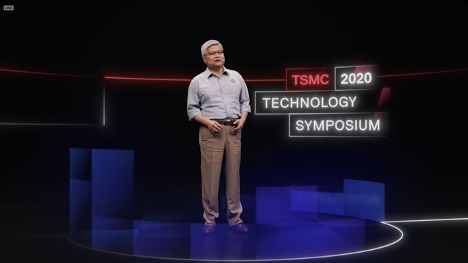
More...
-
08-25-20, 04:37 PM #10740
Anandtech: 2023 Interposers: TSMC Hints at 3400mm2 + 12x HBM in one Package
High-performance computing chip designs have been pushing the ultra-high-end packaging technologies to their limits in the recent years. A solution to the need for extreme bandwidth requirements in the industry has been the shifts towards large designs integrated into silicon interposers, directly connected to high-bandwidth-memory (HBM) stacks.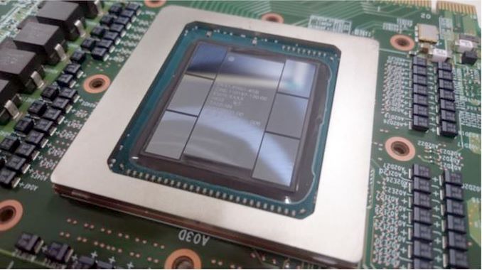
TSMC has been evolving their CoWoS-S packaging technology over the years, enabling designers to create bigger and beefier designs with bigger logic dies, and more and more HBM stacks. One limitation for such complex designs has been the reticle limit of lithography tools.
Recently, TSMC has been increasing their interpose size limitation, going from 1.5x to 2x to even projected 3x reticle sizes with up to 8 HBM stacks for 2021 products.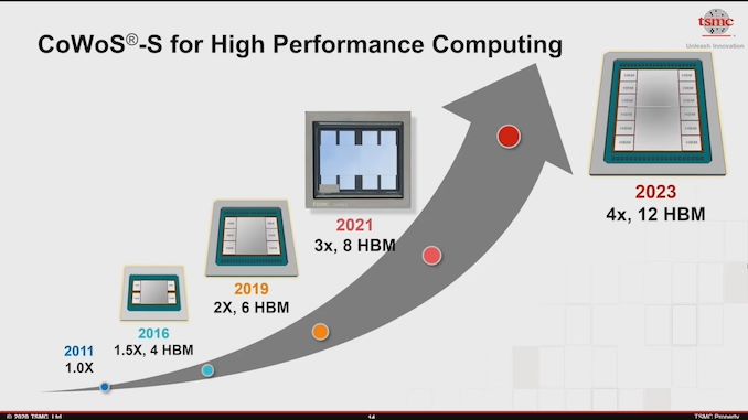
As part of TSMC’s 2020 Technology Symposium, the company has now teased further evolution of the technology, projecting 4x reticle size interposers in 2023, housing a total of up to 12 HBM stacks.
Although by 2023 we’re sure to have much faster HBM memory, a 12-stack implementation with the currently fastest HBM2E Samsung Flashbolt 3200MT/s modules would represent at least 4.92TB/s of memory bandwidth, which is multitudes faster than even the most complex designs today.
Carousel image credit: NEC SX-Aurora TSUBASA with 6 HBM2 Stacks
Related Reading- TSMC Details 3nm Process Technology: Full Node Scaling for 2H22 Volume Production
- TSMC To Build 5nm Fab In Arizona, Set To Come Online In 2024
- TSMC & Broadcom Develop 1,700 mm2 CoWoS Interposer: 2X Larger Than Reticles
- TSMC Boosts CapEx by $1 Billion, Expects N5 Node to Be Major Success
- Early TSMC 5nm Test Chip Yields 80%, HVM Coming in H1 2020
- TSMC: 5nm on Track for Q2 2020 HVM, Will Ramp Faster Than 7nm
- TSMC: N7+ EUV Process Technology in High Volume, 6nm (N6) Coming Soon
More...


 Quote
QuoteThread Information
Users Browsing this Thread
There are currently 35 users browsing this thread. (0 members and 35 guests)


Bookmarks