

Results 10,861 to 10,870 of 12096
Thread: Anandtech News
-
11-10-20, 04:39 PM #10861
Anandtech: Apple Announces The Apple Silicon M1: Ditching x86 - What to Expect, Based
Today, Apple has unveiled their brand-new MacBook line-up. This isn’t an ordinary release – if anything, the step that Apple is making today is something that hasn’t happened in 15 years: The start of a CPU architecture transition across their whole consumer Mac line-up.
Thanks to the company’s vertical integration across hardware and software, this is a monumental change that nobody but Apple can so swiftly usher in. The last time Apple ventured into such an undertaking in 2006, the company had ditched IBM’s PowerPC ISA and processors in favour of Intel x86 designs. Today, Intel is being ditched in favour of the company’s own in-house processors and CPU microarchitectures, built upon the ARM ISA.
The new processor is called the Apple M1, the company’s first SoC design for Macs. With four large performance cores, four efficiency cores, and an 8-GPU core GPU it features 16 billion transistors on the new 5nm process node. Apple’s is starting a new SoC naming scheme for this new family of processors, but at least on paper it does look at lot like an A14X.
Today’s event contained a whole ton of new official announcement, but also lacked (in typical Apple fashion) in detail. Today, we’re doing to be dissecting the new Apple M1 news, as well as doing an microarchitectural deep dive based on the already released Apple A14 SoC.
More...
-
11-10-20, 11:14 PM #10862
Anandtech: Apple Intros First Three Apple Silicon Macs: Late 2020 MacBook Air, 13-I
As previously announced by Apple this summer, the company is embarking on a major transition within its Mac product lineup. After almost a decade and a half of relying on Intel’s x86 processors to serve at the heart of every Mac, the company is going to be shifting to relying on its own, in-house designed Arm processors to power their now un-PC computers. At the time Apple set the start of the transition at the end of this year, and right on cue, today Apple announced the first three Apple Silicon-powered Macs: the Late 2020 editions of the MacBook Air, the 13-Inch MacBook Pro, and the Mac Mini.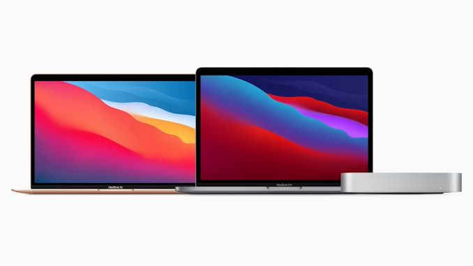
Three of the lower-end devices within the Mac family, Apple is starting small for their Arm transition. The Mac Mini is of course the smallest and most integrated of Apple’s desktop-style computers. Meanwhile the MacBook Air and MacBook Pro are Apple’s two 13.3-inch laptops, focused on portability and performance respectively. Fittingly, these are also the areas where performance-per-watt is generally the most critical, as Apple is very strongly power-constrained on these platforms, and thus performance-limited as well.
More...
-
11-11-20, 01:46 PM #10863
Anandtech: Intel Xe Graphics: An Interview with VP Lisa Pearce
Bringing a new range of hardware to market is not an easy task, even for Intel. The company has an install base of its ‘Gen’ graphics in hundreds of millions of devices around the world, however the range of use is limited, and it doesn’t tackle every market. This is why Intel started to create its ‘Xe’ graphics portfolio. The new graphics design isn’t just a single microarchitecture – by mixing and matching units where needed, Intel has identified four configurations that target key markets in its sights, ranging from the TeraFLOPs needed at the low-end up to Peta-OPs for high performance computing.
Leading up the charge on the driver and software side of the equation is Intel’s Lisa Pearce. Lisa is a 23 year veteran of Intel, consistently involved in Intel’s driver application and optimization, collaboration with independent software vendors, and Lisa now stands as the Director and VP of Intel’s Architecture, Graphics and Software Group, and Director of Visual Technologies. Everything under that bucket of Intel’s Graphics strategy as it pertains to drivers and software, all the way from integrated graphics through gaming and enterprise into high-performance, is in Lisa’s control.
More...
-
11-11-20, 01:46 PM #10864
Anandtech: Intels Xe-HP Now Available to Select Customers
As part of Intel’s next generation Xe graphics strategy, one of the key elements is going to be the offerings for the enterprise market. For commercial enterprises that need hardcore compute resources, the Intel’s Xe-HP products are expected to be competition against Ampere and CDNA. The HP design, as we’ve already seen in teaser photos, is designed to leverage both scale-up and scale-out by using a multi-tile strategy paired with high-bandwidth memory.
As far as we’re aware, Intel’s timeline for Xe-HP is to enable general availability sometime in 2021. The early silicon built on Intel’s 10nm Enhanced SuperFin process is in-house, working, and has been demonstrated to the press in a first-party video transcode benchmark. The top offering is a quad-tile solution, with a reported peak performance somewhere in the 42+ TFLOP (FP32) range in NEO/OpenCL-based video transcode. This would be more than twice as much as NVIDIA’s Ampere A100.
In an announcement today, Intel says that it is offering its dual-tile variant to select customers already, however not directly. Intel is going to offer Xe-HP use through its development cloud infrastructure, DevCloud. Approved partners will be able to spin up instances on Intel’s service, compile, and run Xe-HP compatible software in order to gauge both performance and code adaptability for their workflows.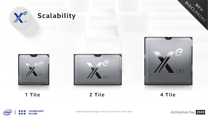
Normally in a situation where a hardware provider offers a cloud-based program for unreleased products, there is a tendency to think that they’re not actually providing the hardware, that it’s an obfuscation on the back-end to what could be a series of FPGAs emulating what the customer thinks they’re using. This is part of the problem with these non-transparent cloud services. However, Intel has confirmed to us that the hardware on the back-end is indeed its Xe-HP silicon, running over a custom PCIe interface and powered through its Xeon infrastructure.
One of the common elements to new silicon is finding bugs and edge cases. All hardware vendors do their own validation testing, however in recent years Intel itself has presented the front where its customers, due to the scale of workloads and deployment, can test far deeper and wider than Intel does – up to a scale of 20-50x. But that’s when those partners have the hardware in hand, perhaps early engineering samples at lower frequencies; by using DevCloud, some of those big partners can attempt some of those workflows in preparation for a bigger direct shipment, and optimize the whole processes.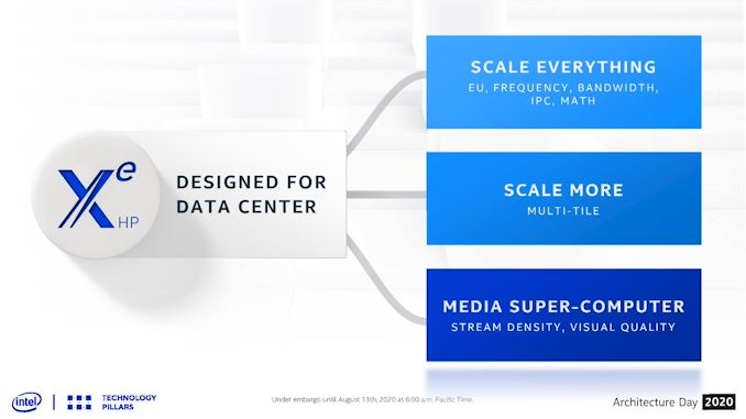
Intel did not state what the requirements were to get access to Xe-HP in the cloud. I suspect that if you have to ask, then you probably don’t qualify. In other news, Intel's Xe-LP solution, Iris Xe MAX, is available in DevCloud for public access.
Related Reading- Intel Xe-HP Graphics: Early Samples Offer 42+ TFLOPs of FP32 Performance
- Spotted At Hot Chips: Quad Tile Intel Xe-HP GPU
- What Products Use Intel 10nm? SuperFin and 10++ Demystified
- The Intel Xe-LP GPU Architecture Deep Dive: Building Up The Next Generation
- Raja Koduri at Intel HPC Devcon Keynote Live Blog (4pm MT, 11pm UTC)
More...
-
11-11-20, 06:07 PM #10865
Anandtech: Western Digital at FMS 2020: Zoned SSDs, Automotive NVMe And More
At Flash Memory Summit this week (online for the first time), Western Digital is showing off three new SSD products and have outlined the company's areas of strategic focus in a keynote presentation.
First up, Western Digital is commercializing NVMe Zoned Namespaces (ZNS) technology with the new Ultrastar DC ZN540 datacenter SSD. We covered ZNS in depth earlier this year after the extension to the NVMe standard was ratified. Western Digital has been one of the strongest proponents of ZNS, so it's no surprise that they're one of the first to launch a zoned SSD product.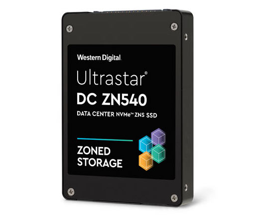
The ZN540 is based on a similar hardware platform to their existing traditional enterprise/datacenter SSDs like the Ultrastar DC SN640 and SN840. The ZN540 is a 2.5" U.2 SSD using 3D TLC NAND and a Western Digital-designed SSD controller, and offers capacities up to 8TB with dual-port PCIe 3.0 support. The most significant hardware difference is a big decrease in the amount of RAM the SSD needs compared to the usual 1GB per 1TB ratio; Western Digital isn't ready to disclose exactly how much RAM they are shipping in the ZN540, but it should be a nice decrease in BOM.
The new ZN540 also renders the Ultrastar DC SN340 mostly obsolete. The SN340 was designed to get some of the benefits of a zoned SSD by using a Flash Translation Layer that works with 32kB blocks instead of the usual 4kB. That enables a DRAM reduction by a factor of eight, at the expense of much lower random write performance, especially for small block sizes. ZNS SSDs simply prohibit random writes in the first place rather than silently deliver horrible performance with extremely high write amplification, and the ZNS interface allows software to be properly informed of these limitations and provides tools to cope with them.
The Ultrastar DC ZN540 is currently sampling to major customers. Software support for ZNS SSDs is fairly mature at the OS level in the Linux kernel and related tooling. Application-level support for zoned storage is more of a work in progress, but Western Digital and others have been hard at work. Zoned storage backends already exist for some well-known applications like the Ceph cluster filesystem and RocksDB key-value database.
Next up, Western Digital is introducing their first industrial-grade NVMe SSD. Western Digital's industrial and automotive lineup currently consists of eMMC and UFS modules and SD/microSD cards. The new Western Digital IX SN530 NVMe SSD is an industrial/automotive grade version of the PC SN530, OEM counterpart to the retail SN550. These are DRAMless NVMe SSDs, albeit some of the best-performing DRAMless SSDs on the market. The IX SN530 will be available with capacities of 256GB to 2TB of TLC NAND, or operating as SLC NAND with capacities of 85-340GB and drastically higher write endurance. One of the main target markets for the IX SN530 will be automotive applications, where the push toward self-driving cars is increasing storage capacity and performance requirements.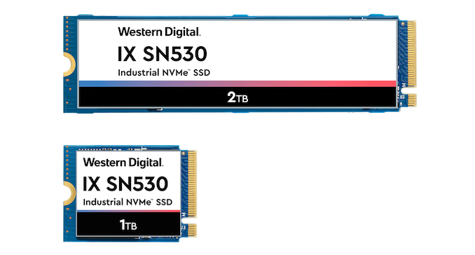
The TLC-based variants of the IX SN530 are sampling now, and the SLC versions will start sampling in January.
Western Digital IX SN530 SSD Specifications Capacity 85 GB 170 GB 340 GB 256 GB 512 GB 1 TB 2 TB Form Factor M.2 2280 or M.2 2230 M.2 2280 Controller WD in-house DRAM None NAND Flash Western Digital 96L SLC Western Digital 96L TLC Sequential Read 2400 MB/s 2400 MB/s 2500 MB/s Burst Sequential Write 900 MB/s 1750 MB/s 1950 MB/s 900 MB/s 1750 MB/s 1950 MB/s 1800 MB/s Sustained Sequential Write 900 MB/s 1750 MB/s 1950 MB/s 140 MB/s 280 MB/s 540 MB/s 525 MB/s Random Read IOPS 160k 310k 410k 160k 310k 410k 370k Random Write IOPS 180k 330k 350k 85k 150k 350k 300k Projected Write Endurance 6000 TB 12000 TB 24000 TB 650 TB 1300 TB 2600 TB 5200 TB
Since the IX SN530 will be available in capacities up to 2TB, Western Digital is also adding a 2TB model to the related WD Blue SN550 consumer NVMe SSD, extending their entry-level NVMe product line now that such high capacities are no longer just for high-end SSDs. The new WD Blue SN550 2TB model is already in production and working its way through the supply chain, so it should be available for purchase soon.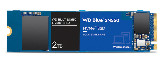
Several performance metrics for the 2TB SN550 are slower than the 1TB model and the write endurance rating didn't scale with capacity, so the 2TB WD Blue SN550 isn't a groundbreaking product. The initial MSRP is quite a bit higher than a DRAMless NVMe SSD should be going for, even accounting for the fact that WD tends to have the best-performing DRAMless SSDs on the market.WD Blue SN550 SSD Specifications Capacity 250 GB 500 GB 1 TB 2 TB Form Factor M.2 2280 PCIe 3.0 x4 Controller WD in-house DRAM None NAND Flash Western Digital/SanDisk 96L 3D TLC Sequential Read 2400 MB/s 2400 MB/s 2400 MB/s 2600 MB/s Sequential Write 950 MB/s 1750 MB/s 1950 MB/s 1800 MB/s Random Read 170k IOPS 300k IOPS 410k IOPS 360k IOPS Random Write 135k IOPS 240k IOPS 405k IOPS 384k IOPS Warranty 5 years Write Endurance 150 TB
0.3 DWPD300 TB
0.3 DWPD600 TB
0.3 DWPD900 TB
0.25 DWPDMSRP $44.99 $53.99 $94.99 $249.99
Western Digital also used their keynote presentation to give a rundown on various areas the company is focusing on as part of their strategy to be more than just a NAND and drive manufacturer.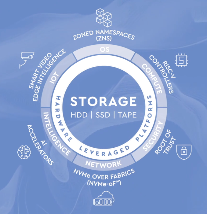
And in fact, we didn't get to hear much at all about their NAND flash memory itself, despite the name of the conference. Western Digital and Kioxia announced their 112-layer fifth-generation BiCS 3D NAND in January 2020, but the new WD drives announced today are still using 96-layer TLC. We did catch a few potential references to future generations of 3D NAND: they have above 100 layers in production now and will reach 200 layers "pretty soon", they'll be moving the peripheral circuits to be above and below the memory rather than alongside (following in the footsteps of Micron, Intel and Hynix), 2Tbit dies will be coming at some point, and I/O speeds going from 400MT/s to 2GT/s over four generations. Since those were all passing mentions, we're hesitant to take any of it as a solid indication of what to expect from their sixth generation 3D NAND, and we certainly don't have any indication of when that will be going into production or hitting the market.
Aside from the Zoned Storage work we've already covered, Western Digital mentioned several areas of ongoing development. They are a big proponent of the RISC-V CPU architecture and have open-sourced some RISC-V core designs already, but we don't have a clear picture of what—if any—Western Digital products have already started using RISC-V CPU cores. NVMe over Fabrics is one of the most important datacenter storage technologies, and Western Digital is participating through their OpenFlex storage systems and the RapidFlex NVMeoF controller technology they acquired last as from Kazan Networks.
Western Digital is talking about computational storage, but only in the broadest terms—reiterating all the tantalizing possibilities, but not yet announcing any specific hardware development plans. In the area of security, Western Digital highlighted their membership in the OpenTitan project for developing open-source hardware root of trust technology. This is driven by the industry consensus that features like Secure Boot aren't just useful for protecting the boot process of your operating system, but for verifying all the intelligent components in a system that handle sensitive data.
More...
-
11-11-20, 06:07 PM #10866
Anandtech: Microchip Announces PCIe 5.0 And CXL Retimers
Microchip is entering the market for PCIe retimer chips with a pair of new retimers supporting PCIe 5.0's 32GT/s link speed. The new XpressConnect RTM-C 8xG5 and 16xG5 chips extend the reach of PCIe signals while adding less than 10ns of latency.
As PCIe speeds have increased, the practical range of PCIe signals across a circuit board has decreased, requiring servers to start including PCIe signal repeaters. For PCIe gen3, mostly-analog redriver chips were often sufficient to amplify signals. With PCIe gen4 and especially gen5, the repeaters have to be retimers that operate in the digital domain, recovering the clock and data from the input signal with awareness of the PCIe protocol to re-transmit a clean copy of the original signal. Without retimers, PCIe gen5 signals only have a range of a few inches unless expensive low-loss PCB materials are used, so large rackmount servers with PCIe risers at the back and drive bays in the front are likely to need retimers in several places.
Microchip's new XpressConnect retimers add less than 10ns of latency, considerably better than the PCIe requirements of around 50–60ns. This also helps make the new XpressConnect retimers suitable for use with CXL 1.1 and 2.0, which use the same physical layer signaling as PCIe gen5 but target more latency-sensitive use cases. These retimers are the first Microchip products to support PCIe 5.0, but the rest of their PCIe product lineup including PCIe switches and NVMe SSD controllers will also be migrating to PCIe gen5.
The XpressConnect retimers come in 8-lane and 16-lane variants, both supporting bifurcation to smaller link widths, so that a single retimer can be used for multiple x1, x2 or x4 links. The retimers conform to Intel's specification for the BGA footprint and pinouts of PCIe retimers (13.4x8.5mm for 8 lanes, 22.8x8.9mm for 16 lanes), so these chips will eventually be competing against alternatives that could be used as drop-in replacements.
Common uses for PCIe retimers will be on drive bay backplanes, riser cards, and on large motherboards to extend PCIe 5.0 to the slots furthest from the CPU. Retimer chips will not necessarily be needed for every PCIe or CXL link in a server, but they are going to be an increasingly vital component of the PCIe ecosystem going forward. PCIe/CXL connections with a short distance from the CPU to the peripheral and few connectors will usually not need retimers, and riser or adapter cards that use PCIe switches to fan out PCIe connectivity to a larger number of lanes will already be re-transmitting signals and thus don't need extra retimers.
Microchip's XpressConnect PCIe 5.0 / CXL 2.0 retimers are currently sampling to customers, and are being incorporated into an Intel reference design for PCIe riser boards. Mass production will begin in 2021.
More...
-
11-12-20, 11:44 AM #10867
Anandtech: Samsung Announces Exynos 1080 - 5nm Premium-Range SoC with A78 Cores
Today Samsung LSI announced the new Exynos 1080 SoC, a successor to last year’s Exynos 980. This year’s 1080 is seemingly positioned a little above the 980 in terms of performance as we’re seeing some quite notable gains in features compared to the 980. It’s to be remembered that this is a “premium” SoC, meaning it’s not a flagship SoC, but it’s also not quite a mid-range SoC, fitting itself in-between those two categories, a niche which has become quite popular over the last 1-2 years.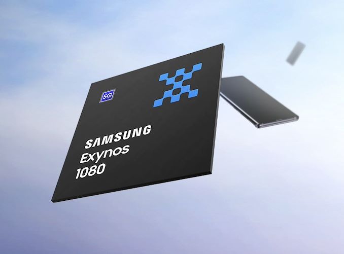
The new SoC is defined by having a new 1+3+4 CPU configuration, as reasonably large GPU, and full 5G connectivity integrated, and is the first publicly announced SoC to be manufactured on Samsung’s new 5LPE process node.
On the CPU side of things, this is the first time we’ve seen Samsung adopt a 1+3+4 CPU configuration, now adopting the Cortex-A78 architecture on the part of the performance cores. One core is clocked at 2.8GHz while the three others are running at 2.6GHz. Qualcomm had first introduced such a setup and it seems it’s become quite popular as it gives the benefit of both performance and power efficiency. The four big cores are accompanied by four Cortex-A55 cores at 2.0GHz.Samsung Exynos SoCs Specifications SoC Exynos 980 Exynos 1080 CPU 2x Cortex-A77 @ 2.2GHz
+ 6x Cortex-A55 @ 1.8GHz1x Cortex-A78 @ 2.8GHz
+ 3x Cortex-A78 @ 2.6GHz
+ 4x Cortex-A55 @ 2.0GHzGPU Mali G76MP5 Mali G78MP10 NPU Integrated NPU + DSP
5.7TOPSMemory
ControllerLPDDR4X LPDDR4X / LPDDR5 Media 10bit 4K120 encode & decode
H.265/HEVC, H.264, VP910bit 4K60 encode & decode
H.265/HEVC, H.264, VP9Modem Shannon Integrated
(LTE Category 16/18)
DL = 1000 Mbps
5x20MHz CA, 256-QAM
UL = 200 Mbps
2x20MHz CA, 256-QAM
(5G NR Sub-6)
DL = 2550 Mbps
UL = 1280 MbpsShannon Integrated
(LTE Category 16/18)
DL = 1000 Mbps
5x20MHz CA, 256-QAM
UL = 200 Mbps
2x20MHz CA, 256-QAM
(5G NR Sub-6)
DL = 5100 Mbps
UL = 1280 Mbps
(5G NR mmWave)
DL = 3670 Mbps
UL = 3670 MbpsWiFi Integrated 802.11ax (WiFi 6) Integrated 802.11ax (WiFi 6) ISP Main: 108MP
Dual: 20MP+20MPMain: 200MP
Dual: 32MP+32MPMfc.
ProcessSamsung
8nm LPPSamsung
5nm LPE
On the GPU side of things, we’re seeing a quite large jump compared to the Exynos 980 as Samsung is now not only moving onto the new Mali-G78 microarchitecture, but is deploying double the number of cores. It’s possible that previous performance of these “premium” tier SoCs was as well received as there was a large gap in performance compared to their flagship SoC counterparts, so Samsung employing a much larger GPU here is quite welcome, and still leaves room for a much larger configuration for their flagship SoC, which has yet to be announced.
Samsung now also includes a new generation NPU and DSP in the design, and quoted machine-learning inference power of 5.7TOPs which is again quite a sweet-spot for such an SoC.
The new modem now is capable of both 5G NR Sub-6 frequencies as well mmWave, something which was lacking in the Exynos 980. Samsung’s decision to deploy mmWave here is interesting given that outside of the US there’s very little deployment in terms of network coverage as sub-6GHz is being prioritised. Samsung adding this in in what’s supposed to be a more cost-effective SoC means that they’re actually expecting it to be used, which is going to be very interesting.
Multi-media wise, the specifications listed for the SoC show that it actually cut down on the MFC (Multi-Function Codec) decoder and encoder capabilities as it’s now only capable of 4K60 instead of 4K120 in the last generation – maybe a further cost optimisation.
The camera ISP capabilities have been improved, supporting now single camera sensors up to 200MP, and dual-sensor operation up to 32+32MP.
The most exciting thing about the SoC is its transition from an 8LPP DUV process to the new 5LPE EUV process. This is Samsung LSI’s and Samsung Foundry’s first announced 5nm chip which is going to garner a lot of attention when it comes to comparisons made against competitor SoCs on TSMC’s 5nm node. I do expect the Samsung process to be less dense, but we’ll have to wait out and see the actual performance and power differences between the two nodes.
Last year I had noted that the Exynos 980 looked like an extremely well balanced SoC and we did see it employed by third-party vendors such as VIVO, as well as more Samsung Mobile devices. The new Exynos 1080 look to be even stronger and solid in terms reaching a balance between performance and features and still trying to optimise things for cost.
Related Reading:- Samsung Announces Exynos 980 - Mid-Range With Integrated 5G Modem
- Samsung Announces Exynos 990: 7nm EUV, M5, G77, LPDDR5 Flagship SoC alongside Exynos 5123 5G Modem
- Samsung Announces the Exynos 9825 SoC: First 7nm EUV Silicon Chip
- ISCA 2020: Evolution of the Samsung Exynos CPU Microarchitecture
- The Samsung Galaxy S20+, S20 Ultra Exynos & Snapdragon Review: Megalomania Devices
More...
-
11-12-20, 11:44 AM #10868
Anandtech: IBM at FMS 2020: Beating TLC With QLC, MRAM And Computational Storage
Two years ago we reported on IBM's FlashCore Module, their custom U.2 NVMe SSD for use in their FlashSystem enterprise storage appliances. Earlier this year IBM released the FlashCore Module 2 and this week they detailed it in a keynote presentation at Flash Memory Summit. Like its predecessor, the FCM 2 is a very high-end enterprise SSD with some unusual and surprising design choices.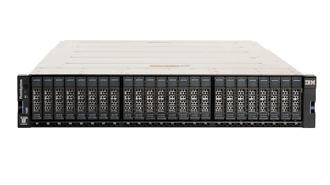
The most unusual feature of the first IBM FlashCore Module was the fact that it did not use any supercapacitors for power loss protection, nor did the host system include battery backup. Instead, IBM included Everspin's magnetoresistive RAM (MRAM) to provide an inherently non-volatile write cache. The FCM 2 continues to use MRAM, now upgraded from Everspin's 256Mbit ST-DDR3 to their 1Gbit ST-DDR4 memory. The higher-density MRAM makes it much easier to include a useful quantity on the drive, but it's still far too expensive to entirely replace DRAM on the SSD: managing the FCM2's multi-TB capacities require several GB of RAM. IBM's main motivation for using MRAM as a write buffer instead of DRAM with power loss protection is that supercaps or batteries tend to have service lifespans of only a few years, and when an energy storage system fails things can get ugly. IBM sees MRAM as offering better long-term reliability that is worth the cost and complexity of building a drive with three kinds of memory.
The FCM 1 used Micron 64-layer 3D TLC NAND, which at the time was a pretty standard choice for high-end enterprise SSDs. The FCM 2 makes the bold switch to using Micron's 96L 3D QLC NAND. The higher density and lower cost per bit has enabled them to double the maximum drive capacity up to 38.4 TB, but maintaining performance while using inherently slower flash is a tall order. Fundamentally, the new NAND has about three times the program (write) latency and 2-3 times the read latency. Write endurance and data retention are also lower. But the FCM 2 is still rated for 2 DWPD and IBM claims increased performance thanks to a combination of several tricks.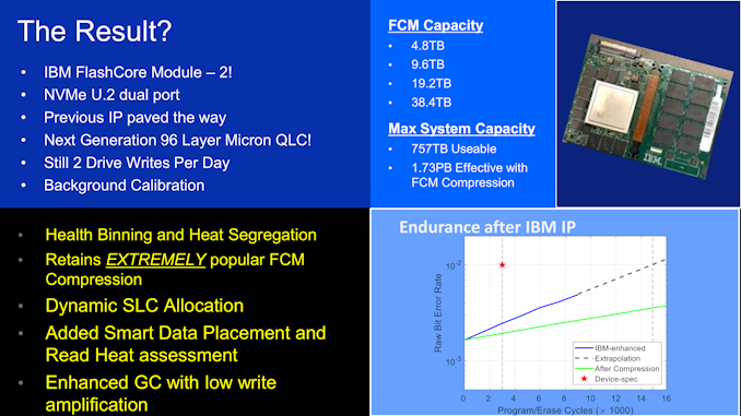
IBM's FlashCore Modules use a custom SSD controller architecture implemented on a massive FPGA. The 20-channel NAND interface explains the slightly odd drive capacities compared to more run of the mill SSDs with 8 or 16 channel controllers. IBM includes line-rate transparent compression derived from the hardware compression provided on IBM Z mainframes. This provides a compression ratio around 2.3x on typical data sets, which goes a long way toward mitigating the endurance issues with QLC (but the FCM 1 also had compression, so this isn't a big advantage for the FCM 2). The FCM 2 also can use some of its QLC NAND as SLC. This isn't as simple as the SLC write caches found on virtually all consumer SSDs. Instead, the FCM 2 tracks IO patterns to predict which chunks of data will be frequently accessed ("hot" data), and tries to store those on SLC instead of QLC while sending "cold" data straight to QLC. Enterprise SSDs typically avoid using SLC caching because it makes it hard to ensure good QoS during sustained workloads. (Client drives can count on real-world workloads offering plenty of idle time that can be used for cache flushing.) IBM seems confident that their smart data placement heuristics can avoid any serious QoS issues, and the FCM 2 drive can also make use of data lifetime hints provided by host software.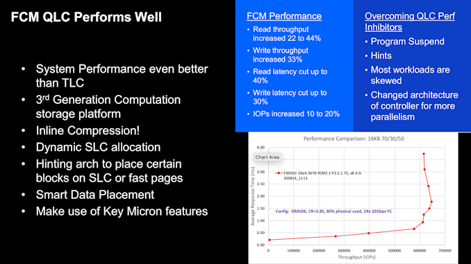
Using the FCM 2 drives, IBB's FlashSystem storage appliances can offer 40GB/s per 2U/24 drive system, with usable capacities of up to 757 TB or an effective capacity of about 1.73 PB thanks to the built-in compression.
More...
-
11-12-20, 06:27 PM #10869
Anandtech: Xilinx and Samsung Launch SmartSSD Computational Storage Drive
At Samsung's Tech Day 2018 they debuted a collaboration with Xilinx to develop Smart SSDs that would combine storage with FPGA-based compute accelerator capabilities. Their proof of concept prototype combining a Samsung SSD and Xilinx FPGA on a PCIe add-in card has evolved into a 4TB U.2 drive that has completed customer qualification and reached general availability.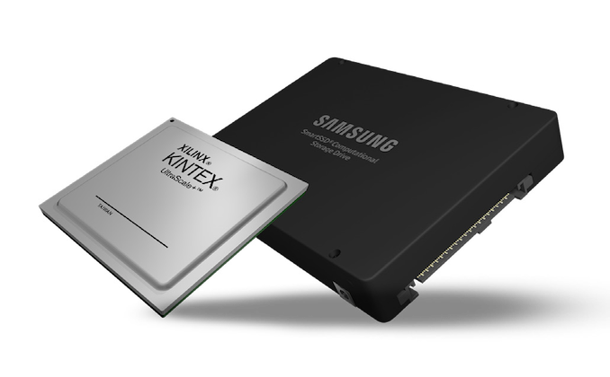
The Samsung SmartSSD CSD includes all the guts of one of their high-end PCIe Gen3 enterprise SSDs, plus the largest FPGA from Xilinx's Kintex Ultrascale+ (16nm) family and 4GB of DDR4 specifically for the FPGA to use. The SmartSSD CSD uses a portion of the FPGA as a PCIe switch, so the FPGA and SSD each appear to the host system as separate PCIe endpoints and all PCIe traffic going to the SSD is first routed through the FPGA.
In a server equipped with dozens of large and fast SSDs, actually trying to make use of all that stored data can lead to bottlenecks with the CPU's IO bandwidth or compute power. Putting compute resources on each SSD means the compute capacity and bandwidth scales with the number of drives. Classic examples of compute tasks to offload onto storage devices are compression and encryption, but reconfigurable FPGA accelerators can help with a much broader range of tasks.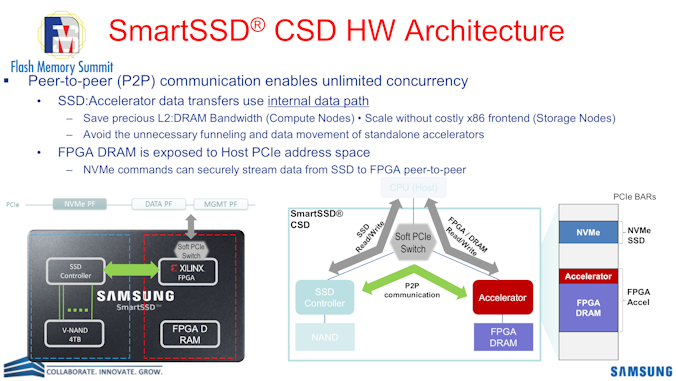
Xilinx has been building up a library of IP for storage accelerators that customers can use with the SmartSSD CSD, as part of their Vitis libararies of building blocks and and Xilinx Storage Services turnkey solutions. Samsung has worked with Bigstream to implement Apache Spark analytics acceleration. Third party IP that has been developed for Xilinx's Alveo accelerator cards can also be ported to the SmartSSD CSD thanks to the common underlying FPGA platform, so IP like Eideticom's NoLoad CSP are an option.
The Samsung SmartSSD CSD is being manufactured by Samsung and sold by Xilinx, initially with 3.84TB capacity but other sizes are planned.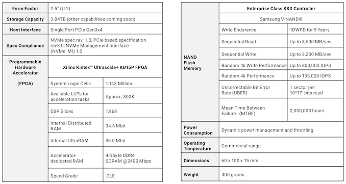
More...
-
11-12-20, 06:27 PM #10870
Anandtech: Highpoint Updates NVMe RAID Cards For PCIe 4.0, Up To 8 M.2 SSDs
HighPoint Technologies has updated their NVMe RAID solutions with PCIe 4.0 support and adapter cards supporting up to eight NVMe drives. The new HighPoint SSD7500 series adapter cards are the PCIe 4.0 successors to the SSD7100 and SSD7200 series products. These cards are primarily aimed at the workstation market, as the server market has largely moved on from traditional RAID arrays, especially when using NVMe SSDs for which traditional hardware RAID controllers do not exist. HighPoint's PCIe gen4 lineup currently consists of cards with four or eight M.2 slots, and one with eight SFF-8654 ports for connecting to U.2 SSDs. They also recently added an 8x M.2 card to their PCIe gen3 family, with the Mac Pro specifically in mind as a popular workstation platform that won't be getting PCIe gen4 support particularly soon._575px.jpg)
HighPoint's NVMe RAID is implemented as software RAID bundled with adapter cards featuring Broadcom/PLX PCIe switches. HighPoint provides RAID drivers and management utilities for Windows, macOS and Linux. Competing software NVMe RAID solutions like Intel RST or VROC achieve boot support by bundling a UEFI driver in with the rest of the motherboard's firmware. Highpoint's recent 4-drive cards include their UEFI driver on an Option ROM to provide boot support for Windows and Linux systems, and all of their cards allow booting from an SSD that is not part of a RAID array. HighPoint's NVMe RAID supports RAID 0/1/10 modes, but does not implement any parity RAID options.
Highpoint has also improved the cooling on their RAID cards. Putting several high-performance M.2 SSDs and a power-hungry PCIe switch on one card generally requires active cooling, and HighPoint's early NVMe RAID cards could be pretty noisy. Their newer heatsink design lets the cards benefit from airflow provided by case fans instead of just the card's own fan (two fans, for the 8x M.2 cards), and the fans they are now using are a bit larger and quieter.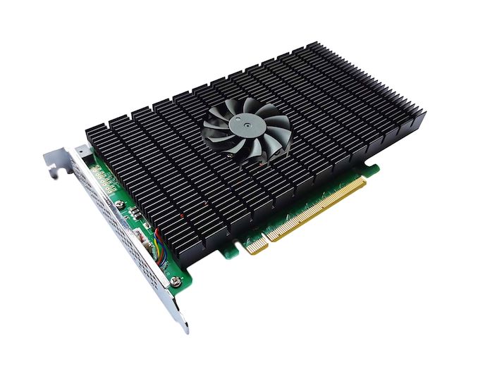
In the PCIe 2.0 era, PLX PCIe switches were common on high-end consumer motherboards to provide multi-GPU connectivity. In the PCIe 3.0 era, the switches were priced for the server market and almost completely disappeared from consumer/enthusiast products. In the PCIe 4.0 era, it looks like prices have gone up again. Even though these cards are the best way to get lots of M.2 PCIe SSDs connected to mainstream consumer platforms that don't support the PCIe port bifurcation required by passive quad M.2 riser boards, the pricing makes it very unlikely that they'll ever see much use in systems less high-end than a Threadripper or Xeon workstation. However, Highpoint has actually tested on the AMD X570 platform and achieved 20GB/s throughput using Phison E16 SSDs, and almost 28GB/s on an AMD EPYC platform (out of a theoretical limit of 31.5 GB/s). These numbers should improve a bit as faster, lower-latency PCIe 4.0 SSDs become available.
Now that consumer M.2 NVMe SSDs are available in 4TB and 8TB capacities, these RAID products can accommodate up to 64TB of storage at a much lower price per TB than using enterprise SSDs, and without requiring a system with U.2 drive bays. For tasks like audio and video editing workstations, that's an impressive amount of local storage capacity and throughput. The lower write endurance of consumer SSDs (even QLC drives) is generally less of a concern for workstations than for servers that are busy around the clock, and for many use cases having a capacity of tens of TB means the array as a whole has plenty of write endurance even if the individual drives have low DWPD ratings. Using consumer SSDs also means that peak performance is higher than for many enterprise SSDs, and a large RAID-0 array of consumer SSDs will have a total SLC cache size in the TB range.HighPoint NVMe RAID Adapters Model SSD7505 SSD7540 SSD7580 SSD7140 Host Interface PCIe 4.0 x16 PCIe 3.0 x16 Downstream Ports 4x M.2 8x M.2 8x U.2 8x M.2 MSRP $599 $999 $999 $699
The SSD7140 (8x M.2, PCIe gen3) and the SSD7505 (4x M.2, PCIe gen4) have already hit the market and the SSD7540 (8x M.2, PCIe gen4) is shipping this month. The SSD7580 (8x U.2, PCIe gen4) is planned to be available next month.
More...


 Quote
QuoteThread Information
Users Browsing this Thread
There are currently 54 users browsing this thread. (0 members and 54 guests)


Bookmarks