

Results 11,011 to 11,020 of 12091
Thread: Anandtech News
-
02-15-21, 12:35 PM #11011
Anandtech: Xbox Series X SoC: Power, Thermal, and Yield Tradeoffs
This week at ISSCC (International Solid State Circuits Conference), Microsoft presented a talk titled ‘Xbox Series X SoC: A Next Generation Gaming Console’, with hardware engineer Paul Paternoster presenting. The 30 minute presentation covered a lot about Microsoft’s latest console processor, most of which was a repeat about what we saw at Hot Chips in August last year, however there was a new element in this presentation talking about how the console design team balanced acoustics, power, thermal performance, and processor yield, discussing where the hotspots in the design originate and where the performance/power targets of the final silicon were optimized.
More...
-
02-16-21, 09:31 AM #11012
Anandtech: Lenovo ThinkStation P620 Review: A Vehicle for Threadripper Pro
The workstation line of machines from Lenovo have been extremely successful for the company. While ThinkStation might not have as much brand identity as the more recognizable ThinkPad, for the markets that require them Lenovo’s ThinkStation range has been at the front of high-performance under-the-desk offerings since 2008. Lenovo has focused on everything from small form factor entry ThinkStation systems, all the way up to high-end dual socket P-series tower designs. The system we are reviewing today actually marks a major milestone for the ThinkStation business; the ThinkStation P620 is Lenovo’s first AMD workstation system, and it comes in to replace the whole range of Intel-based high-performance ThinkStations previously offered.
More...
-
02-17-21, 08:02 AM #11013
Anandtech: The Samsung 870 EVO (1TB & 4TB) Review: Does the World Need Premium SATA S
Samsung is one of the few brands still launching new high-end SATA SSDs in the consumer market. The new Samsung 870 EVO is a fine update to a very successful product line, but sticking with their long-time strategy of being the premium option doesn't make much sense when NVMe has taken over the high-end SSD market segment.
More...
-
02-18-21, 11:15 AM #11014
Anandtech: NVIDIA Nerfs Ethereum Hash Rate & Launches CMP Dedicated Mining Hardware
One of the critical points during this period of high demand for graphics cards is that a portion of them are being purchased by professional users looking to mine cryptocurrencies. The recent launch of new cards coupled with record highs in the cryptocurrency market has led to a rebirth of the mining community, who as of recently could earn ~$15 per RTX 3090 graphics card. These professional miners buy graphics card by the pallet load, sometimes bypassing retailers and going direct to distributors, as they can guarantee a complete shipment sale in one go. The knock on effect is fewer cards available for gamers looking to build new systems, leading to empty shelves and causing prices to spike for the handful of cards that ever make it to retailers.
In order to at least offer a fig leaf to gamers, in the past certain graphics board partners started producing mining-only graphics cards. These had no graphical outputs, making them almost impossible for gaming use cases, but it filtered off some of the mining market into buying those rather than taking stock away from shelves for gamers. This was a poor band-aid, and now NVIDIA has gone one step further to separate mining from gaming.
NVIDIA’s announcement today is two-fold: firstly addressing the upcoming launch of the RTX 3060 graphics on February 25th, and secondly announcing a new range of dedicated mining hardware.
RTX 3060: Halving the Mining Rate
One of the key drivers as to why the new graphics cards are being sold is because they are so good at doing the mining operations for various cryptocurrencies (namely for Ethereum and other derived coins) and earning the users a semblance of return on their purchase. Mining requires hardware and software, and it’s the software side that NVIDIA is tackling with this first announcement.
For the upcoming RTX 3060, the software drivers for this graphics card will automatically limit cryptocoin hashing rates to half – making how much they can earn specifically halved. The software drivers will do this by detecting the math coming through the pipeline and restricting access to the hardware for those operations. At this point we’re not sure if it’s a cut in frequency that the drivers will cause or simply limiting the operations to half of the hardware, but either way NVIDIA is hoping this will detract professional miners from buying these cards if the return on them is halved.
No plans are being announced for cards currently in the market, perhaps because the drivers for those cards already allow a full-rate compute solution, and those can simply keep older drivers installed.
NVIDIA CMP: Dedicated Mining Silicon for Ethereum
In the same way that ‘crypto’ cards without video outputs were pushing into the market for balance, NVIDIA is going a step further and removing the video outputs from the silicon entirely. There are other potential optimizations that could be made for power and performance, but at this point NVIDIA is simply stating as graphics-less silicon. This could be a mix of customized new silicon, or simply silicon already manufactured that had defects in the video output pipeline.
The new NVIDIA CMP HX dedicated mining cards will come in four variants up to 320 W, and from authorized partners including ASUS, Colorful, EVGA, Gigabyte, MSI, Palit, and PC Partner. These cards (along with drivers) are also set to be designed such that more of these cards can be enabled in a single system.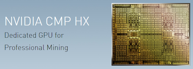
What’s interesting here is that these states aren’t that great. Here is a breakdown of what NVIDIA’s cards do today, and you can see why:NVIDIA CMP HX Mining Hardware AnandTech 30HX 40HX 50HX 90HX Eth Hash Rate* 26 MH/s 36 MH/s 45 MH/s 86 MH/s Rated Power 125 W 185 W 250 W 320 W Reference Connectors 8-pin 8-pin 2 x 8-pin 2 x 8-pin Memory Size 6 GB 8 GB 10 GB 10 GB Availability Q1 Q1 Q2 Q2 *NVIDIA Measured to DAG and Epoch 394
The only way these new CMP HX mining add-in cards make financial sense is if they are really cheap, around $600 for the 90HX, otherwise the retail gaming GPUs seem to be a lot more efficient.NVIDIA Hardware Hash Rates AnandTech Hash Rate Power Efficiency
MH/s/WRTX 3090 121 MH/s 290 W 0.42 RTX 3080 98 MH/s 224 W 0.44 90HX 86 MH/s 320 W 0.27 RTX 3070 62 MH/s 117 W 0.53 RTX 3060 Ti 60 MH/s 120 W 0.50 RTX 2080 Ti 49 MH/s 240 W 0.20 50HX 45 MH/s 250 W 0.18 40HX 36 MH/s 185 W 0.19 30HX 26 MH/s 125 W 0.21 HX Data from NVIDIA
RTX Data from Minerstat
NVIDIA isn’t giving any more details on when these mining add-in cards will be made available, aside from Q1 for the slower ones and Q2 for the faster ones. No word on pricing, nor on distribution methods – there’s a chance here that these cards will only be sold by distributors direct to professional mining outlets. By the pallet. Note that this doesn’t stop the high demand for power supplies. That market is also feeling the effects.
Related Reading- NVIDIA’s GeForce RTX 3060 Gets a Release Date: February 25th
- NVIDIA Reveals GeForce RTX 3060: Launching Late February For $329
- The NVIDIA GeForce CES 2021 Live Blog: Game On
- Launching This Week: NVIDIA’s GeForce RTX 3060 Ti, A Smaller Bite of Ampere For $400
- Launching This Week: NVIDIA’s GeForce RTX 3070; 1440p Gaming For $499
- NVIDIA Announces the GeForce RTX 30 Series: Ampere For Gaming, Starting With RTX 3080 & RTX 3090
More...
-
02-19-21, 10:04 AM #11015
Anandtech: 2021 NAND Flash Updates from ISSCC: The Leaning Towers of TLC and QLC
The annual IEEE International Solid-State Circuits Conference covers a range of topics of interest to AnandTech. Every year the conference includes a session on non-volatile memories where most of the NAND flash memory manufacturers share technical details of their latest developments. At the conference we get more information than these companies are usually willing to share in press briefings, and the presentations are usually about technology that will be hitting the market during the coming year.
At ISSCC 2021 this week, four of the six major 3D NAND flash memory manufacturers are presenting their newest 3D NAND technology. Samsung, SK hynix and Kioxia (+Western Digital) are sharing their latest 3D TLC NAND designs and Intel is presenting their 144-layer 3D QLC NAND. Not participating this year are Micron (who announced their 176L 3D NAND late last year) and Chinese newcomer YMTC.
3D TLC (3-bit per cell) Updates
Samsung, SK hynix, and Kioxia/WD presented information about their upcoming generations of 3D TLC. Not shown here is Micron's 176L TLC, because they haven't released most of this data for their latest generation of 3D NAND.
Unsurprisingly, it looks likely that Samsung will again be in the lead for performance, with the lowest read latency and fastest write speeds. However, their bit density is still clearly lagging even though they're claiming a 70% jump with this generation. In the past, their lagging density hasn't been as much of a downside as it might appear at first glance, because Samsung has been able to avoid using string stacking and can manufacture a stack of 128 layers as a single deck while their competitors have all had to split their stack into two decks, increasing the number of fab steps required. This might be the generation that brings Samsung's inevitable adoption of string stacking, but if that's the case then their lingering density disadvantage is rather disappointing. On the other hand, if they've managed to put off that transition for one more generation and achieved this kind of density increase only using a combination of other techniques (most notably a CMOS under Array layout), then it's a very impressive advance and it would be safe to say that Samsung is years ahead of the competition when it comes to the high aspect ratio etching of the vertical channels that is the most critical fab step in scaling 3D NAND. We'll know more once Samsung discloses the actual layer count, but they're keeping that secret for now—which hints that they don't expect to have the highest layer count to brag about.3D TLC NAND Flash Memory
ISSCC PresentationsSamsung SK hynix Kioxia (Toshiba)
WDYear Presented at ISSCC 2021 2019 2021 2021 2019 2018 Layers 128 176 >170 128 96 Die Capacity 512 Gb 512 Gb 512 Gb 1 Tb 512 Gb 512 Gb Die Size (mm2) 101.58 98 66 86 Density (Gbit/mm2) 8.5 5 10.8 10.4 7.8 5.95 IO Speed 2.0 Gb/s 1.2 Gb/s 1.6 Gb/s 2.0 Gb/s 1.066 Gb/s 533 Mb/s Program Throughput 184 MB/s 82 MB/s 168 MB/s 160 MB/s 132 MB/s 57 MB/s Read Latency (tR) 40 µs 45 µs 50 µs 50 µs 56 µs 58 µs Erase Block Size 24 MB 18 MB Planes 4? 2 4 4 4 2 CuA / PuC Yes No Yes Yes Yes No
The TLC parts described by SK hynix and Kioxia/WD look fairly similar, save for the big difference that SK hynix is talking about a 512Gb die and Kioxia is talking about a 1Tb die. Both designs look to have similar performance and density, though Kioxia is touting a higher NAND interface speed. Kioxia and Western Digital have put out a press release announcing 162-layer 3D NAND, so they're a bit behind SK hynix and Micron for total layer count. That press release also mentions a 10% improvement in the horizontal density of their cell array, so Kioxia and Western Digital are probably packing the vertical channels closer together than any of their competitors.
3D QLC (4-bit per cell) Updates
The only company with updates this year on QLC is Intel.
In general, Intel has been more focused on QLC NAND than any of its competitors. This 144L QLC is the first generation of 3D NAND Intel hasn't co-developed with Micron, and it is unique in several respects. Intel is taking its 3D NAND technology in different directions from the rest of the industry will have interesting ramifications for their agreement to sell the NAND flash business to SK hynix, but in the short term it seems like Intel is getting the NAND they want to be selling. With only 144 layers, Intel is almost certainly now in the last place for total layer count. Compared to 9x-layer QLC, Intel has much better performance and density—but QLC versions of the new TLC described by SK hynix and Kioxia should have comparable density. Intel has backed off from the frankly astronomical erase block size their 96L QLC used, but the 48MB block size of their new 144L QLC still seems a bit high.3D QLC NAND Flash Memory
ISSCC PresentationsIntel Samsung SK hynix Kioxia
WDYear Presented at ISSCC 2021 2020 2020 2018 2020 2019 Layers 144 96 92 64 96 96 Die Capacity 1 Tb 1 Tb 1 Tb 1 Tb 1 Tb 1.33 Tb Die Size (mm2) 74.0 114.6 136 182 122 158.4 Density (Gbit/mm2) 13.8 8.9 7.53 5.63 8.4 8.5 IO Speed 1.2 Gb/s 800 Mb/s 1.2 Gb/s 1.0 Gb/s 800 Mb/s 800 Mb/s Program Throughput 40 MB/s 31.5 MB/s 18 MB/s 12 MB/s 30 MB/s 9.3 MB/s Program Latency (tPROG) 1630 µs 2080 µs 2 ms 3 ms 2.15 ms 3380 µs Read Latency
(tR)Avg 85 µs 90 µs 110 µs 145 µs 170 µs 160 µs Max 128 µs 168 µs 165 µs Erase Block Size 48 MB 96 MB 16 MB 24 MB 24 MB Planes 4 4 2 2 4 2
CMOS Under Array From Everyone
Intel and Micron's now-dissolved joint venture was the second NAND flash manufacturer to make the switch to 3D NAND, after Samsung. The most significant innovation the Intel/Micron 3D NAND brought to the industry was the CMOS Under the Array (CuA) design. This places most of the NAND die's peripheral circuitry—page buffers, sense amplifiers, charge pumps, etc.—under the vertical stack of memory cells instead of alongside.
This change saves a big chunk of die space and allows for over 90% of the die area to be used for the memory cell array. SK hynix was next to make this switch, which they call "Periphery under Cell" (PuC). The rest of the manufacturers are now also onboard: Kioxia (then Toshiba) and Western Digital presented a 128-layer CuA design at ISSCC 2019 but their fifth generation BiCS 3D NAND ended up going into production as a 112L design without CuA. Their ISSCC presentation this year is for a "170+" layer design with CuA, and they've put out a press release confirming that their sixth generation BiCS 3D NAND will be a 162-layer design with CuA.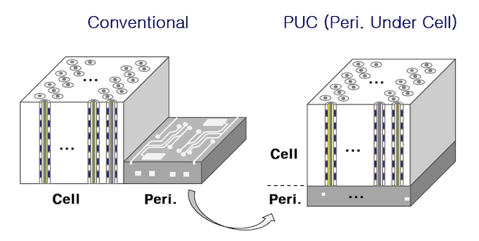
Aside from saving die space, a CuA/PuC style design for 3D NAND allows for a die to include more peripheral circuitry than would otherwise be cost-effective. This makes it practical to divide a die's memory array into more separate planes, each with their own copies of much of the peripheral circuitry. Most 3D NAND that has been built without a CuA layout has used just two planes per die, but now that everyone is using CuA the standard is four planes per die. This provides extra parallelism that increases the performance per die and offsets the overall SSD performance drop that usually comes from using fewer dies to reach the same total capacity.
A CuA structure is not without its challenges and downsides. When a manufacturer first switches to CuA they get a big increase in available die space for peripheral circuitry. But after that, each successive generation that adds layers means there's less die space available for managing the same number of memory cells, so peripheral circuitry still has to shrink. Putting peripheral circuitry under the memory cell array also introduces new constraints. For example, Samsung's ISSCC presentation this year mentions the challenges of constructing large capacitors for the charge pumps when they can no longer use the tall metal structures that are simple to include alongside the 3D NAND stack.
Better On-Die Parallelism: Four Planes Per Die
Dividing a NAND flash die into four planes allows for the die to handle more operations in parallel, but doesn't make it behave quite like four independent dies. There are restrictions on what can be done in parallel: for example, simultaneous writes still have to go to the same word line within each plane. But as the number of planes in a flash die grows, manufacturers have been working to loosen some of those restrictions. In previous years, manufacturers have introduced *independent* multi-plane reads, meaning simultaneous reads in different planes don't have any restrictions on the locations within each plane that are being read—a big win for random read throughput.
Now, another restriction on multi-plane operations is being relaxed: the timing of read operations in different planes doesn't need to line up. This makes it possible for one plane to perform multiple reads from SLC pages while another plane is performing a single slower read from TLC or QLC pages. This capability is called Asynchronous Independent (Multi-)Plane Read. The practical effect is that for read operations, a large 4-plane die can now match the performance of four smaller 1-plane dies. This mitigates many of the performance downsides that higher per-die capacity brings to SSDs that only have one or two dies per channel.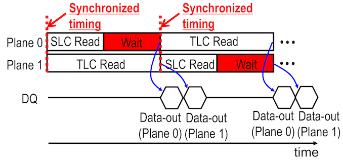
Kioxia and WD reported that implementing this capability required them to stop sharing charge pumps between planes, in order to avoid poorly-timed voltage and current fluctuations that would have resulted from unsynchronized read operations. Intel is also halfway to this capability with their 4-plane 144L QLC: planes are paired up into plane groups, and each plane group can perform reads without needing to align with the timing of reads in the other plane group.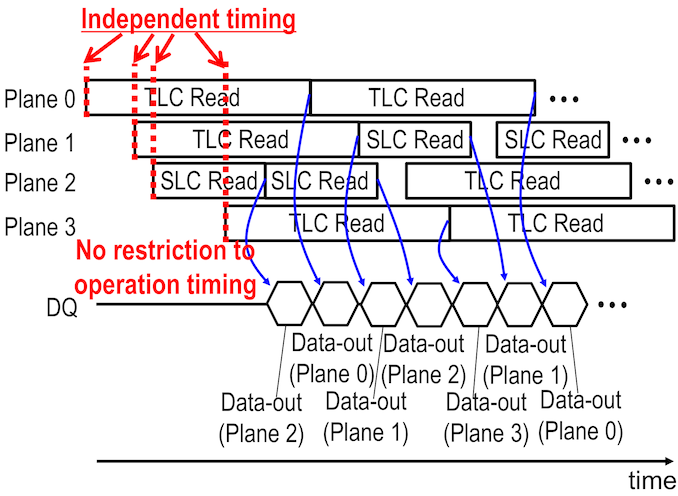
NAND IO Speeds Outpacing SSD Controller Support
The new TLC NAND parts described at ISSCC support IO speeds ranging from 1.6 to 2.0 Gb/s for communication between the NAND flash dies and the SSD controller. The fastest NAND in SSDs currently on the market runs at 1.2-1.4Gb/s. The NAND manufacturers can benefit from vertical integration by ensuring that their own SSD controller designs used for their own SSDs will be ready to support these higher IO speeds, but other SSD vendors that rely on third-party controllers may be left behind. Phison's latest E18 8-channel controller for high-end PCIe 4.0 SSDs only supports 1.2Gb/s IO speeds, and their upcoming E21T 4-channel NVMe controller supports 1.6Gb/s. Silicon Motion's 8-channel SM2264 and 4-channel SM2267 support 1.6Gb/s and 1.2Gb/s IO speeds respectively.
Since 8 channels running at 1.2Gb/s is already enough for a SSD to saturate a PCIe 4.0 x4 connection, these new higher IO speeds will not be of much use to high-end SSDs until PCIe 5.0 arrives. But more affordable 4-channel consumer SSD controllers will be able to use these higher speeds to move up well into PCIe 4.0 performance territory, matching or exceeding the throughput that the first PCIe 4.0 SSD controller (Phison E16, 8ch @ 800Mb/s) offered. As demonstrated by drives like the SK hynix Gold P31, an advanced 4-channel controller supporting high IO speeds on each channel can be very competitive on performance while operating with far higher power efficiency than 8-channel controllers.
Hitting these higher IO speeds requires major upgrades to the interface logic on the NAND dies, and as we've seen with other high-speed interfaces like PCI Express, increasing power consumption is a major concern. Samsung is addressing this by using dual-mode drivers and termination. When higher drive strength is needed because of more load on the bus (from more dies per channel), the'll use a PMOS transistor for pull-up, and otherwise they can use a NMOS transistor and cut the power consumption of the driver by more than half. This gives Samsung a single interface design that will work well for both small consumer SSDs and large enterprise drives with many more dies per channel. (In the past Samsung has added separate retimer dies to multi-chip packages that stack lots of NAND dies together on the same one or two channels. We're not sure if Samsung is still using this technique.)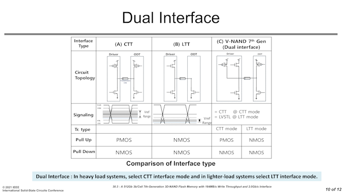
String Stacking: First Triple-Deck NAND
String stacking has been viewed as something of a necessary evil for scaling up 3D NAND to higher layer counts. Only Samsung has managed to build more than 100 layers of 3D NAND at a time, and everyone else has long since switched to stacking two decks each with a more reasonable layer count. This means that eg. Micron's 176-layer 3D NAND is built as 88 layers of memory cells, then another 88 layers are constructed on top. This drives up cost compared to doing all the layers at once, and it requires careful alignment at the interface between decks. But the alternative would be to make the vertical channels much wider, so that the aspect ratio (width vs depth) would stay within the realm of what can be feasibly etched by current fab techniques.
Intel's 144L QLC design includes the surprise that they are already moving to a 3-deck stack: 48+48+48 layers rather than the 72+72 we would expect. Since their previous generation is a 48+48 layer (96L total) design, it's possible that they have changed very little about how the memory array itself is fabricated aside from repeating the same sequence of deposition, etch and fill steps a third time. Intel is taking a hit on fab throughput with this approach, but it probably helps them better control the variation in channel and cell dimensions from the top to bottom of the stack, which may be more of a concern given their focus on QLC and their unique decision to still use a floating gate memory cell rather than switching to a charge trap cell like everyone else.
To go along with this triple-deck structure, Intel has reorganized how they handle erase blocks, and now each of the three decks constitutes a separate collection of erase blocks. That means the middle third of a 144L string can now be erased without interfering with the data stored in the other two thirds of the string. Dividing blocks by decks is also how Intel was able to reduce the 96 MB block size with their 96L QLC down to a less extreme 48MB block size.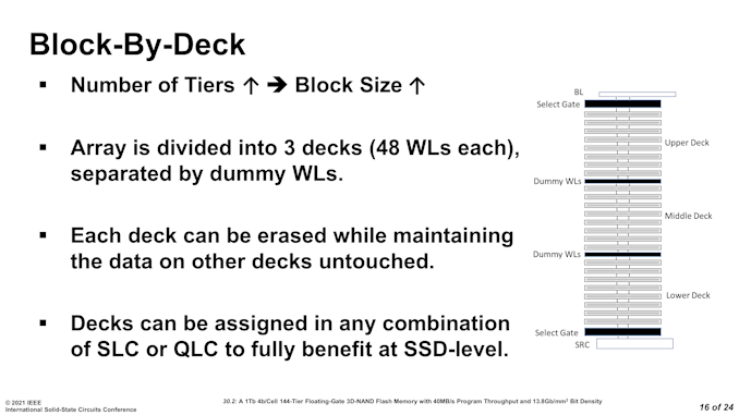
A Small Caveat about Academic Conferences
It's important to understand that ISSCC, where these updates are presented, is an academic conference. The presentations are not product announcements and the papers are not product spec sheets. The designs presented at ISSCC don't always match what goes into mass production. For example, Kioxia/WD in the past have presented designs for 128L and "170+" layer NAND, but their actual fifth and sixth generation BiCS NAND as mass produced are 112L and 162L designs. They also, despite mentioning it in their 2019 talk, deferred a switch to a more dense 'CMOS under Array (CuA) structure' to a later product line. Specifications such as write performance are also often presented as best-case, and real world products end up being a notch below what is presented.
Despite the coming together of all these companies under one conference, even when the presentation does match the eventual product, what we learn from ISSCC is usually imperfect and incomplete information. The companies are inconsistent about what metrics they report, and we usually get information for only one die design per generation—a company might present their 512Gbit design even if they're planning to manufacture both 512Gbit and 256Gbit parts. In recent years several companies seem to be alternating between talking about their QLC one year and TLC the next. In spite of all of that, ISSCC presentations on 3D NAND are still a great way to gauge how the state of the art has progressed and where the industry as a whole is headed.
About half the content of these presentations is clever schemes for micromanaging voltages applied to various wires to optimize the read, program and erase processes. There are complex tradeoffs between speed, accuracy, wear and other factors. we're not going to dig into all of these details, other than to say that programming a cell to the desired voltage (and without disturbing other cells) is not a simple process, and even reading from a TLC or QLC cell is quite a bit more complicated than reading from a DRAM or SRAM cell. We're more interested in any major structural changes in the dies themselves, and the end results of all the finessing of voltages: the speeds at which a page of memory can be read or programmed.
Source Material: 68th ISSCC, Feb 13-22nd 2021
More...
-
02-19-21, 10:04 AM #11016
Anandtech: Toshiba Unveils World's First FC-MAMR HDD: 18 TB, Helium Filled
Toshiba this week announced the industry's first hard drive featuring flux-control microwave-assisted magnetic recording (FC-MAMR) technology. The new MG09-series HDDs are designed primarily for nearline and enterprise applications, they offer an 18 TB capacity along with an ultra-low idle power consumption.
The Toshiba MG09-series 3.5-inch 18 TB HDD are based on the company's 3rd generation nine-platter helium sealed platform that features 18 heads with a microwave-emitting component which changes magnetic coercivity of the platters before writing data. The HD disks are made by Showa Denko K.K. (SDK), a long-time partner of Toshiba. Each aluminum platter is about 0.635 mm thick, it features an areal density of around 1.5 Tb/inch2 and can store up to 2 TB of data. The MG09 family also includes a 16 TB model which presumably features a lower number of platters (based on the same performance rating).
For modern enterprise and nearline 3.5-inch HDDs, Toshiba's MG09-series drives uses a motor with a 7200-RPM spindle speed. The HDDs are also equipped with a 512 MB buffer and are rated for a 281 MB/s maximum sustained data transfer rate. Unfortunately, Toshiba has not updated the random access performance of the new products, though it is likely that their per-TB IOPS performance is lower when compared to predecessors. The manufacturer will offer its new drives both with SATA 3.3 (6 Gbps) and SAS 3.0 (12 Gbps) interfaces as well as a selection of logical data block length.
One of the noteworthy things about Toshiba's MG09-series FC-MAMR HDDs is their power consumption. In active idle mode, they typically consume 4.16/4.54 Watts (SATA/SAS models), which is considerably lower when compared with Seagate's Exos X18 as well as Western Digital's Ultrastar DC HC550. As far as power consumption efficiency at idle (large hard drives could spend plenty of time idling) is concerned, the 18 TB MG09 is an undeniable champion consuming just 0.23 Watts per TB (in case of the SATA version). Meanwhile, the new drives are rated for 8.35/8.74 Watts (SATA/SAS SKUs) during read/write operations, which is higher when compared to the DC HC550 as well as predecessors from the MG07 and the MG08-series.
As the MG09 family of hard drives are intended for datacenter racks that accommodate hundreds of vibrating HDDs, they feature numerous enhancements to ensure consistent performance, reliability, and durability. Typically such enhancements include top and bottom attached motors, RVFF, as well as environmental sensors. Like all modern drives for 24/7 applications, Toshiba's MG09-series units are rated for a 550 TB average annualized workload, 2.5 million hours MTBF, and are covered with a standard five-year warranty.Brief Specifications of Toshiba's MG09 HDDs Capacity 18 TB 16 TB Platters 9 8 Heads 18 16 Recording Technology Flux-control microwave-assisted
magnetic recording (FC-MAMR)RPM 7200 RPM Interface SATA 6 Gbps/SAS 12 Gbps DRAM Cache 512 MB Persistent Write Cache Yes Helium-Filling Yes Sequential Data Transfer Rate (host to/from drive) 281 MB/s MTBF 2.5 million Rated Annual Workload 550 TB Acoustics (idle) 20 dB Power Consumption Random read/write SATA: 8.35 W
SAS: 8.74 WIdle SATA: 4.16 W
SAS: 4.54 WWarranty 5 Years
Also, the new MG09 hard drives support Toshiba’s persistent write cache (PWC) with power loss protection (PLP) technology, which is crucial for 4K sector drives that emulate 512B sectors. The PWC with PLP feature guards data in case of power loss while performing read-modify-write (RMW) operation to align the source write request with the physical sectors it has to modify. This capability allows the company to address its clients who run legacy systems that still require high capacities. Also, the new MG09 family includes Sanitize Instant Erase (SIE) and Self Encrypting Drive (SED) models.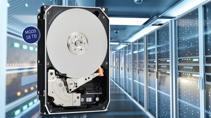
Toshiba has been working on its MG09-series FC-MAMR HDDs for at least two years already. Last year the company said it had made 'significant investments in manufacturing facilities' and promised to start shipments of its 18 TB hard drives by March 31, 2021. This week the company reaffirmed its plan and said it would begin sample shipments of its 18 TB MG09-series MAMR HDDs 'at the end of March 2021.'
Source: Toshiba
More...
-
02-22-21, 02:29 PM #11017
Anandtech: The Samsung Galaxy S21 Ultra & S21 Review: The Near Perfect and The Differ
Today we’re reviewing the Galaxy S21 Ultra in both Exynos and Snapdragon SoC flavours, as well the baseline Galaxy S21 – contrasting two very different devices in Samsung’s new series, coming in at two very different price points.
More...
-
02-22-21, 02:29 PM #11018
Anandtech: AMD To Probe Potential USB Connectivity Issue on Ryzen Systems
Some AMD users have been posting on social media, including Reddit, about experiencing intermittent connectivity problems when using USB ports on their 500-series motherboards. In response, AMD has reached out through a Reddit post that it has been made aware of the connectivity issues, and is requesting more information from specific users with the issue to help them resolve it. Since this announcement, many users have been reaching out to AMD.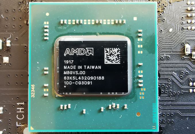
AMD's X570 motherboards have been readily available since July 2019, and its B550 models have been available since June 2020 and have both become well established over the course of the last year and a half. The fact that users are now having USB issues begs the question whether the issues have been present all along but are now rising above the noise, or there is something related to the longevity of these systems.
AMD 500 Series Motherboard and USB Connectivity Issues?
The most common reproduction of this issue appears to be during the use of Virtual Reality headsets such as the Oculus Rift and HTC Vive, with an intermittent connection issue being more prevalent to these users. As USB is the main method to power and communicate with VR headsets and peripherals, any dropout, even slightly to the high-powered VR applications, would instantly be highlighted. That isn't the only problem it can cause, as streaming devices and USB audio interfaces could also experience power dropouts, which could be quite noticeable, especially if doing a recording.
While AMD hasn't pinpointed the exact cause of the issue yet, it asks its users to reach out to them over on Reddit by u/AMDOfficial, which is an official support channel for AMD. Extensively combing through user comments on Reddit, it doesn't seem to be solely related just to one section of hardware. Some of the issues that users report seem to stem from the release of PCIe 4.0 graphics cards on 500 series motherboards. Reddit user u/duddy32 also states that they have been having these issues with a B450 motherboard and a Ryzen 7 3700X processor, which precede the 500-series chipset.
One possible workaround touted to reduce (but importantly not completely stop) the issues is users changing the motherboards' settings from PCIe 4.0 to PCIe 3.0. Users on Reddit have been reporting although it has reduced the frequency of dropouts, it hasn't eliminated them, which could point to an issue between the USB hub controller and other parts of the chipset. Some users are also reporting the issue to be primarily on USB 2.0 ports, and some have had success by switching devices to USB 3.1 ports. It is also recommended to update the firmware to the latest AGESA version on models, which could reduce issues. Although at this point, it's possible to presume that none of the workarounds could fix these problems users are experiencing with random and intermittent USB cutouts.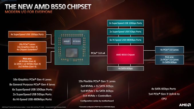
AMD's B550 Chipset layout, including USB connectivity.
Although AMD hasn't notified the reddit audience if it has been able to pinpoint the issue internally, it is asking users experiencing these issues to detail their hardware configurations and other relevant system information to allow AMD to recreate the issues on its end. AMD is also openly encouraging users to directly raise online service requests with AMD customer support to help correlate data and compare notes with other support claims to narrow down the problem potentially.
It should be noted that not all users have experienced these issues - we've tested several dozen AMD AM4 motherboards and have used them extensively over the last 15 months, with exactly zero issues related to this. This is why this issue might only be being highlighted now - either users haven't noticed the issue, as a very slight cutout from a mouse or keyboard may not be very apparent, or they might be lucky that this issue doesn't affect them. However, enough users are coming forward with these intermittent USB connectivity issues to make the issue widespread across multiple models and processor combinations. This means the issue isn't specifically down to a certain manufacturer and looks more like an issue with AMD's chipset or how it connects from the USB hub to the chipset.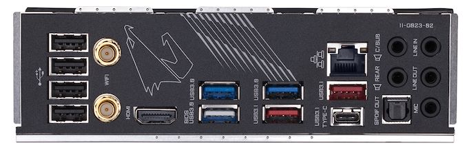
The rear panel of an X70 motherboard with USB 3.1, USB 3.0, and USB 2.0 ports.
If AMD does manage to pinpoint the issue with its in-house team and collaboration of consistent data points provided by its users, it's possible a future AGESA firmware update could alleviate the issues. Of course, if it is directly related to a design and hardware problem, which could be a much tougher nut to crack for AMD.
AMD's official statement posted on 02/20/21 can be found on Reddit here - https://www.reddit.com/r/Amd/comment...th_500_series/
Related Reading- The AMD X570 Motherboard Overview: Over 35+ Motherboards Analyzed
- The AMD B550 Motherboard Overview: ASUS, GIGABYTE, MSI, ASRock, and Others
- AMD Zen 3 Ryzen Deep Dive Review: 5950X, 5900X, 5800X and 5600X Tested
- Investigating Performance of Multi-Threading on Zen 3 and AMD Ryzen 5000
- AMD Precision Boost Overdrive 2: Adaptive Undervolting For Ryzen 5000 Coming Soon
More...
-
02-23-21, 09:13 AM #11019
Anandtech: Lenovo Updates ThinkPads: New Intel and AMD Processors, New Displays, New
Today Lenovo is announcing a slew of updates across a large portion of their ThinkPad lineup, and updating their business-focused products for 2021. Some of the big changes for this year are impressive and welcome, with Lenovo committing to bringing feature-parity between their AMD and Intel offerings, as well as refreshing some of their laptops with 5G, Wi-Fi 6E, and continuing the trend of bringing back 16:10 aspect ratio displays for a better productivity experience.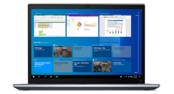
ThinkPad X13 and X13 YogaAlthough some of the ThinkPad X lineup got refreshed back at CES, Lenovo is continuing the 2021 updates today on the X13 and X13 Yoga products, and the changes make these already impressive devices even more so.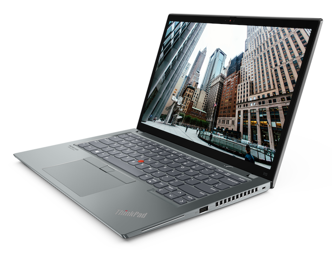
On the processor side, Lenovo is offering either 11th Gen Intel Core – aka Tiger Lake – processors with vPro optional, as well as AMD Ryzen 5000 Pro options. Lenovo says they have heard the feedback from customers and are working hard to close the feature and option gap between the two platforms. For the most part, customers choosing AMD or Intel will have the same specifications and options available for the rest of the product, such as displays, memory, and so on, other than the platform specific features such as Intel supporting Thunderbolt 4 and PCIe 4.0.
The X13 and X13 Yoga will also be getting Wi-Fi 6E meaning 6 GHz support, and for those that want connectivity when out and about, sub-6 5G is an option on the X13, or 4G is available on both models.
Lenovo is also continuing to move to 16:10 displays, with the taller displays filling out more of the body and providing more vertical pixels for productivity. This is a great trend, and one that should not have taken this long to come back to, as of course the original widescreen ThinkPads were all 16:10 before the entire industry moved to 16:9. Lenovo is also proud to offer low-blue light hardware support on the displays, and unlike most low-blue light technologies which cause a red-shift on the display, the backlight physically produces less of the stressful blue lights, allowing the display to still keep the proper white balance.
As this is a proper business machine, there is also addition security such as Match-On-Chip fingerprint readers built into the power button, and the Intel models will support Human Presence Detection which allows the machine to lock when you are away and unlock when you get back. This will be through the IR camera, and as far as the visual camera, Lenovo is including an option for both HD with IR, as well as FHD with IR, the latter being a nice addition thanks to the increase in video conferencing over the last year.
The updated ThinkPad X13 will be available in May starting at $1139 USD, and the X13 Yoga will be available in April starting at $1379.
ThinkPad T14, T14s, and T15When most people imagine ThinkPad, they likely think of the venerable T Series. Lenovo said they are working on feature parity between Intel and AMD, and one of the changes is not branding the products differently based on the CPU, but for the T series, it doesn’t look like they’ve quite gotten there yet. There will be ThinkPad T14 i, ThinkPad T14s i, and ThinkPad T15 powered by Intel, and for the 14-inch models, the ones branded without the i will be AMD Ryzen based.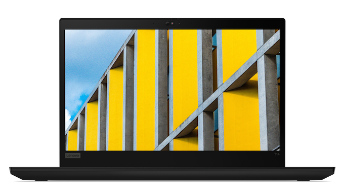 ThinkPad T14
Although the T series is, at least for this gen, sticking with 16:9 aspect ratios, with several options for the 14-inch and 15-inch range including UHD displays with Dolby Vision. Lenovo is also offering its PrivacyGuard displays for extra security, and some low-power options depending on how you configure it.
As far as performance, the laptop will offer up to Core i7 11th Gen with vPro options, or AMD Ryzen 5000 Pro. Memory will be up to 32 GB on the S model, and up to 48 GB on the non-S. Storage is up to 2 TB of PCIe storage, with the Intel platforms supporting PCIe 4.0 speeds. The non-S model T14 and the T15 also offers an optional NVIDIA GeForce MX450 with 2 GB of GDDR6, if extra graphics compute is needed over the Intel Iris Xe or AMD Vega 8 graphics. ThinkPad T14s
As with much of the ThinkPad lineup, Lenovo is offering Wi-Fi 6, 6E, and cellular capabilities with 4G and 5G options. As with the ThinkPad X13 range, Lenovo will also be offering FHD webcams with IR as optional upgrades.
Although the T14s is smaller and lighter than the T14, it includes a larger battery at 57 Wh, compared to just 50 Wh in the larger model. The 15-inch T15 also has the 57 Wh battery.
The ThinkPad T14s is one of my favorite laptops around, and it is always nice to see it get updated. The new models will be available starting in March and going through May depending on the model, with prices starting at $1149 for the ThinkPad T14 AMD model.
ThinkPad P14s and P15sAlso getting an update is a couple of the mobile workstation models under the P-Series, and as with the other units there will be both 11th Gen Intel Core with vPro as well as AMD Ryzen 5000 Pro CPU offerings.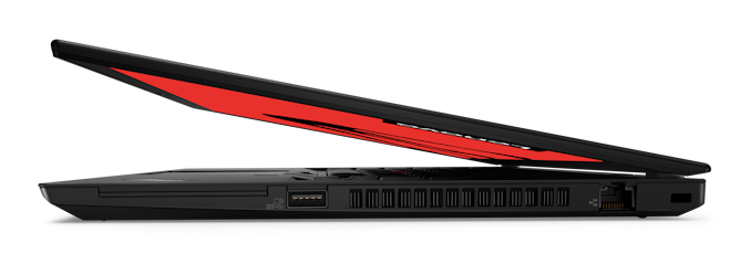
The P14s and P15s will both offer 8 GB or 16 GB of soldered memory, as well as a SO-DIMM slot, which will allow for up to 48 GB maximum memory in these thinner and lighter versions of the P-series laptops. Lenovo is also offering the NVIDIA T500 which is the workstation class graphics based on the Turing MX450 and featuring 4 GB of VRAM.
Both the P14s and P15s will offer FHD displays as standard, with a few options such as ePrivacy or Low-Power, and both will offer an optional UHD display with HDR 400 and Dolby Vision HDR. The UHD displays will come with X-Rite factor color calibration.
For those that need a Linux version, Lenovo will be offering Ubuntu 20.04 LTS installs, as well as Red Had as factory options.
Wireless will be Intel Wi-Fi 6E for 6 GHz support thanks to the Intel AX210 on the Tiger Lake models, and the AMD offerings will still support Wi-Fi 6, but without the 6 GHz support.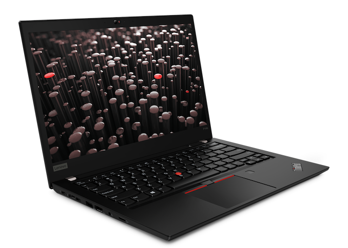
Although some of the other ThinkPads are being offered with a FHD webcam, the P14s and P15s are not, at least for now. The newer webcam is physically larger, and would take a more comprehensive redesign of the chassis, but the HD webcam does offer IR if needed.
The Intel powered P14s i, and the P15s will be available in March, starting at $1389 for either, with the AMD powered P14s coming in May, and starting at $1169.
ThinkPad L14 and L15Rounding out the lineup is the least-expensive way to get into a ThinkPad, and that is the L Series. Also being offered in a L14/15 i Intel based, or L14/15 AMD based design, the least expensive offerings still offer some powerful options.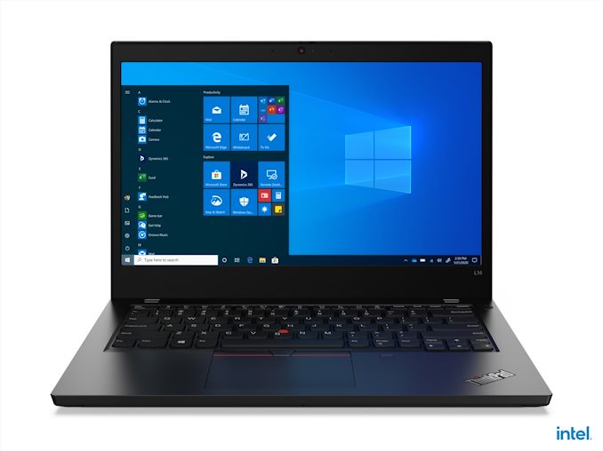
With 11th gen Intel Core with vPro, and AMD Ryzen 5000, there will be two SODIMM slots, thanks to the thicker and heavier design, which means the least expensive models here can be outfitted with the most RAM, at up to 64 GB. There will be Intel Iris Xe, or AMD Vega graphics, and purchasers can opt for NVIDIA GeForce MX 450 as well.
One of the sad realities of a budget device is the display, and the base model comes with a (Yuck) 1366x768 TN panel. Luckily Lenovo offers FHD IPS offerings on both.
Storage is up to 1 TB PCIe SSD, or up to 2 TB spinning hard drive, but you do get Wi-Fi 6 across the range, and optional cellular options.
The L series is really all about entry price, and the new L14 and L15 will be available in May starting at $689.
Source: Lenovo
More...
-
02-23-21, 09:13 AM #11020
Anandtech: Lenovo Introduces The ThinkVision P40w: 40-inch Thunderbolt 4 Display With
Alongside a raft of ThinkPad updates, Lenovo is also announcing a new monitor to pair nicely with those Thinkpads. The Lenovo ThinkVision P40w is a rather impressive looking product, offering a 39.7-inch 21:9 panel, featuring a 5120x2160 WUHD resolution. And that’s not all.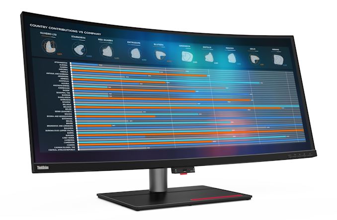
The new P40w is also a dock for your laptop, thanks to the single-cable Thunderbolt 4 port which can charge the laptop at up to 100 Watts. It can provide up to 12 ports from the monitor, including two Thunderbolt 4 ports, and one USB Type-C. Not only that, but Lenovo includes an eKVM, which allows you to control two devices from this single monitor and dock combination. The extra Thunderbolt 4 port also would allow you to daisy-chain another 5K monitor.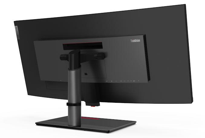
The 21:9 panel offers 98% of the P3 color space, and is factory calibrated for an error level of less than 2.0, and includes hardware-level blue light reduction, to keep the proper white balance while still reducing blue light emissions.Lenovo ThinkVision P40w Specification Display Display Size 39.7-inches
2.0 mm bezels top/sidesResolution 5120x2160 WUHD 75 Hz
140 PPICurvature 2500R Color Gamut 98% P3
Factory CalibratedBrightness 300 nits
1000:1 Contrast IPSResponse Time 4 ms (Extreme Mode)
6 ms (Normal Mode)Ports (Video) 2 x Thunderbolt 4
1 x HDMI 2.0
1 x DisplayPort 1.4
1 x 3.5 mm Audio OutPorts (I/O) Output Ports:
4 x USB 3.2 Gen 1 Type-A
1 x USB 3.2 Gen 1 Type-C
1 x Thunderbolt 4
Input Ports:
1 x USB 3.2 Gen 1 Type-B
1 x Thunderbolt 4
RJ-45Power Delivery USB Type-C : Up to 27 W
Thunderbolt 4: Up to 100 WPower Consumption 60 Watts (Typical)
0.5 Watts Sleep ModeTilt (`)-5° to 22° Swivel 45° Plus/Minus VESA 100 x 100 and 200 x 100 Weight 14.65 kg / 32.30 lbs with stand
There is a built-in RJ-45 jack as well, allowing the monitor to be your network hub, and it supports Wake-On-LAN, PXE, and MAC pass-through. Lenovo is the first manufacturer to retail a professional monitor with Intel Active Management Technology built-in to integrate with the vPro on ThinkPads, and provide the extra management capabilities that provides.
If you have always wanted a big monitor with high resolution, wide gamut support, and of course the management capabilities of Intel AMT, Lenovo has you covered.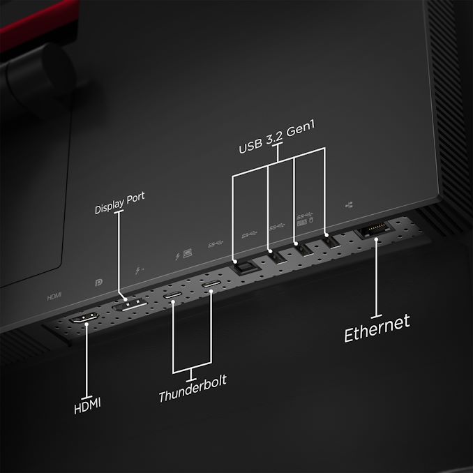
The new ThinkVision P40w will be available in June, starting at $1699 USD.
More...


 Quote
QuoteThread Information
Users Browsing this Thread
There are currently 18 users browsing this thread. (0 members and 18 guests)


Bookmarks