

Results 11,071 to 11,080 of 12089
Thread: Anandtech News
-
03-30-21, 05:20 PM #11071
Anandtech: Kingston Introduces NV1 Entry-Level NVMe SSD
As previewed at CES, Kingston's newest entry-level consumer NVMe SSD is now shipping. The new NV1 uses a similar strategy to Kingston's entry-level SATA drives like the A400, where Kingston is not guaranteeing a specific set of internal components and expects to mix controllers and NAND to hit the cheapest price points. That results in very conservative performance and endurance specifications: sequential transfers around 2GB/s and endurance ratings around 0.2 DWPD for three years.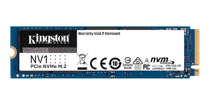
The Kingston NV1 uses DRAMless SSD controllers like the Phison E13T and Silicon Motion SM2263XT, which are both getting a bit old but are still sufficient to offer a step up from SATA performance. The NAND will tend to be TLC on the smaller capacities and QLC for at least the 2TB model, but realistically Kingston could use either type of NAND on any of the capacities depending on what kind of leftover NAND they have lying around.Kingston NV1 SSD Specifications Capacity 500 GB 1 TB 2 TB Form Factor M.2 2280 PCIe 3.0 x4 Sequential Read (MB/s) 2100 Sequential Write (MB/s) 1700 Warranty 3 years Write Endurance 120 TB
0.2 DWPD240 TB
0.2 DWPD480 TB
0.2 DWPDLaunch Price $63.70
(13¢/GB)$115.70
(12¢/GB)$224.90
(11¢/GB)
The NV1 is a more low-end drive than Kingston's existing A2000 NVMe SSD, which uses TLC NAND and has DRAM, but uses the 4-channel SM2263 controller rather than a more mainstream 8-channel controller. The NV1 does reflect the market's shift toward higher capacities, with the product line starting at 500GB and going up to 2TB. We expect retail prices for the NV1 will end up cheaper than the A2000, but for the moment the pricing direct from Kingston is only marginally cheaper.
More...
-
03-30-21, 05:20 PM #11072
Anandtech: Mushkin Launches DELTA And GAMMA PCIe 4.0 NVMe SSDs
Mushkin has announced two new product lines for PCIe 4.0 M.2 SSDs. Following on from last year's introduction of the ALPHA series, the new DELTA and GAMMA drives continue Mushkin's recent trend of using Phison's SSD controllers and reference designs. The ALPHA uses the Phison E12S controller and QLC NAND, the new DELTA uses the Phison E16 controller and QLC NAND, and the new GAMMA uses the Phison E18 controller and TLC NAND.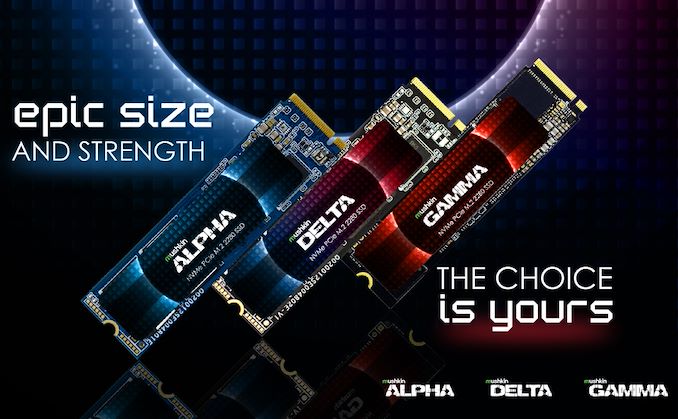
The new Mushkin DELTA series and their existing ALPHA series both use QLC NAND, but the DELTA is not a complete replacement for the ALPHA. The DELTA does offer a performance boost due to the faster controller supporting PCIe 4.0, but that faster Phison E16 controller also takes up more PCB area than the compact Phison E12S controller used in the ALPHA. That prevents the DELTA series from offering an 8TB option. The ALPHA series is focused specifically on extreme capacities since it only includes 4TB and 8TB models, while the DELTA is a bit more mainstream with 1TB through 4TB capacities.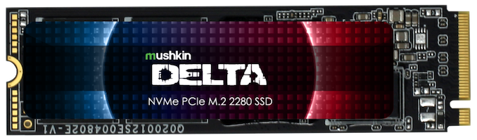
Mushkin DELTA Specifications Capacity 1 TB 2 TB 4 TB Form Factor M.2 2280 PCIe 4.0 x4 Controller Phison E16 NAND Flash 3D QLC Sequential Read (MB/s) 4700 4975 Sequential Write (MB/s) 2100 3750 3975 Random Read IOPS (4kB) 195k 380k 700k Random Write IOPS (4kB) 510k 650k Warranty 5 years Write Endurance 200 TB
0.1 DWPD400 TB
0.1 DWPD800 TB
0.1 DWPDLaunch Price $159.99
(16¢/GB)$299.99
(15¢/GB)$599.99
(15¢/GB)
The new GAMMA series is Mushkin's new flagship based on the Phison E18 controller. Performance specs are similar to other drives based on the same reference design, with sequential read speeds of over 7 GB/s and peak sequential write speeds starting at over 5.5 GB/s for the 1TB model.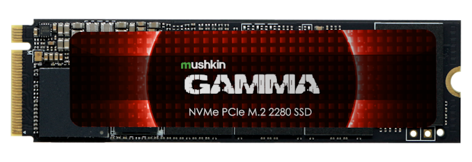
For both the DELTA and GAMMA series, Mushkin's initial pricing is in line with street prices for other drives based on the same hardware. Among that club, Corsair's MP600 CORE and MP600 PRO SSDs come with substantial heatsinks, while Mushkin is following the approach taken by Sabrent, Inland and other brands by keeping the drives slim and leaving any heatsink up to the end user.Mushkin GAMMA Specifications Capacity 1 TB 2 TB Form Factor M.2 2280 PCIe 4.0 x4 Controller Phison E18 NAND Flash 3D TLC Sequential Read (MB/s) 7150 7175 Sequential Write (MB/s) 5600 6800 Random Read IOPS (4kB) 360k 640k Random Write IOPS (4kB) 645k 630k Warranty 5 years Write Endurance 700 TB
0.4 DWPD1400 TB
0.4 DWPDLaunch Price $259.99
(26¢/GB)$499.99
(25¢/GB)
Mushkin hasn't specified the exact NAND used in these new drives, but we expect them to both be using 96-layer 3D NAND. Later this spring we will see a new round of high-end Phison E18 drives adopting Micron's 176-layer 3D TLC for marginal performance improvements, but it's still a bit early for Mushkin to be including the new NAND on the GAMMA.
More...
-
03-31-21, 09:04 AM #11073
Anandtech: Computex 2021 Physical Show Cancelled; Virtual Event Still Taking Place
When it comes to technology tradeshows, one of the biggest early victims of the coronavirus outbreak was Computex, the annual PC-centric trade show in Taiwan. After the 2020 show was delayed and then canceled entirely, event organizer TAITRA vowed to come back with a proper tradeshow in 2021. However, even with vaccinations well underway, it’s become clear that it’s not going to be possible to hold the physical show this year either. As a result, the physical Computex tradeshow has once again been cancelled.
In a very brief news release, TAITRA noted that with the pandemic still ongoing, and border controls preventing international travel, it would not be possible to hold the show in 2021.
With another wave of coronavirus pandemic across the world, it doesn't look like we are close to the end. The majority of the show's stakeholders, including international exhibitors, visitors, and media, cannot join the show due to border control. Therefore, the organizers of COMPUTEX have decided to cancel the onsite exhibition this year.The silver lining, at least, is that while the physical show TAITRA wanted to hold won’t be happening, their parallel virtual show, #COMPUTEXVirtual, will continue on as planned. Scheduled to run for a full month, from May 31st to June 30th, #COMPUTEXVirtual will be the show’s first attempt at doing a large-scale virtual event. The virtual show was originally scheduled to run alongside the physical show, but now with the physical show cancelled, it has become the de facto plan B. At this point it’s not clear who will be presenting and what with the virtual show, and undoubtedly vendors and organizers are scrambling to draw up new plans in light of the physical show’s cancellation.
None the less, even a virtual Computex could stand to be a major show. With a strong and ongoing demand for electronics, the lack of a 2020 show, and CES 2021 being a relatively modest event earlier this year, vendors have been eager to roll out new products – and to do so in front of an audience. So we’ll see how things pan out over the next two months.
More...
-
03-31-21, 06:32 PM #11074
Anandtech: EUV Pellicles Ready For Fabs, Expected to Boost Chip Yields and Sizes
Foundries started limited usage of extreme ultraviolet (EUV) lithography for high-volume manufacturing (HVM) of chips in 2019. At the time, ASML's Twinscan NXE scanners were good enough for production, but the full EUV ecosystem was not quite there. One of the things that impacted EUV was the lack of protective pellicles for photomasks, which limited usage of EUV tools and affected yields. Fortunately, the situation with pellicles has finally improved thanks to the recent introduction of production-ready EUV pellicles, and matters promise to get even better in the coming years.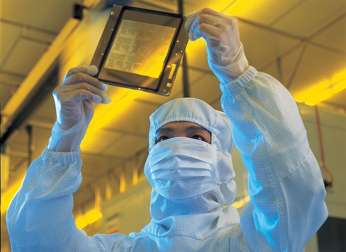
Protecting Precious Reticles
ASML has made a great progress with its Twinscan NXE EUV lithography tools in the recent years, improving performance of light source, availability time, and productivity. Its industry peers have also done a lot to make high-volume manufacturing (HVM) using EUV equipment possible. Still, the EUV ecosystem needs to develop further. One of the most notorious challenges the semiconductor supply chain faced with EUV is development of pellicles that were not available two years ago, which is why TSMC and Samsung Foundry had to invent ways how to use their EUV scanners without protective films.
Pellicles protect 6×6-inch photomasks (reticles) during the chip production flow by sealing them away from particles that could land on their surface, which would otherwise damage them or introduce defects to wafers in production. Each reticle for an EUV tool costs $300,000, so chipmakers are eager to protect them against damage by particles or even the EUV radiation itself as this lowers their costs. Meanwhile, reducing risks associated with yields is perhaps even more important.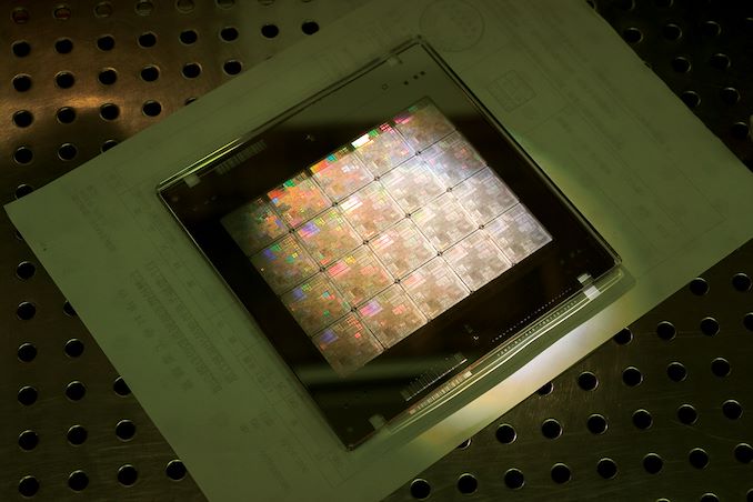
For Reference: A 16nm TSMC Pellicle With Reticle
The need for pellicles, in turn, varies depending on the manufacturer and the types of photomasks employed. Intel, which is known for its big CPU dies, tends to use single-die reticles, which means that just one mask defect introduced by a particle automatically kills the whole die. Meanwhile, if a 25-die photomask is used, a particle adder will 'only' result in 4% lower yield (one dead die), which is why it's been possible to get away without pellicles for smaller chips and multi-die photomasks.
ASML Leading the Pack. For Now
The industry started to develop protective films for EUV tools relatively late after it transpired that nobody can guarantee that an ultra-complex EUV scanner is 100% free of harmful particles, which is why they were not ready in 2019.
Pellicles for photomasks to be used with deep ultraviolet (DUV) lithography equipment are common and cheap. By contrast, since photomasks for EUV are different from photomasks for DUV (EUV masks are essentially 250 to 350-nm thick stacks featuring 40 to 50 alternating layers of silicon and molybdenum on a substrate), pellicles for such reticles are also quite different. In particular, the very short wavelength of EUV means that pellicles for it have a number of requirements that make them uneasy to produce and expensive. EUV pellicles have to be extremely thin, should not affect reflection characteristics of reticles, should feature a high transmission rate (the higher the rate, the higher is productivity of a scanner), should sustain high EUV power levels, and withstand extreme temperatures (from 600ºC to 1,000ºC in the future).
"Most materials absorb very strongly at the more energetic 13.5nm EUV wavelength and, even when the most EUV-transparent materials are selected, the membranes must be extremely thin to approach 90% transmittance," said Emily Gallagher, a principal member of technical staff at Imec. "Such thin membranes are not usually capable of maintaining sufficient strength to be free-standing at the required dimensions. Additionally, the EUV scanner environment is not compatible with many materials and will subject the pellicle to pump-vent cycles."
To date, a number of EUV pellicle options have emerged, according to SemiEngineering:
- ASML introduced its first EUV pellicles in 2019 and licensed the technology to Mitsui Chemicals, which intends to start their volume sales in Q2 2021. Since then, ASML has improved its pellicles.
- Imec has disclosed test results of its pellicles based on carbon nanotubes.
- Graphene Square, Freudenberg Sealing Technologies (FST), and some universities are developing their own pellicles.
So far, only ASML has managed to create commercially viable pellicles for EUV tools that are actually available. ASML's pellicles are based on polysilicon that is 50 nm thick. Back in 2016, they demonstrated a 78% transmissions rate on a simulated 175W source. Currently ASML can sell a pellicle with an 88% transmission rate. And shortly, Mitsui will start supplying such pellicles in volume.
ASML's latest prototypes made of metal silicide demonstrate a 90.6% transmission rate with 0.2% non-uniformities and less than 0.005% reflectivity on a 400W source.
"This upgrade supports our roadmap, which eventually will take source power up to 400 Watts," said Raymond Maas, ASML’s product manager for pellicles, in an interview with Bits&Chips.nl. "The pellicle heats up to 600ºC at that power level, which the polysilicon couldn’t withstand."
By contrast, Imec's prototype pellicles have a transmission rate of 97.7%. In fact, in the long term, when more advanced light sources are available, more sophisticated pellicles will be needed and this is where Imec's carbon nanotubes-based pellicles will come into play.
"Few materials have the potential of high EUV transmission beyond 90% and even fewer materials are at the same time compatible with EUV powers beyond 600W. In addition, the pellicle needs to be strong to be suspended over a large area of the mask (~110mm x 140mm)," said Joost Bekaert, a researcher from Imec.
Unfortunately, it is unclear when Imec's carbon nanotube-based pellicles will be ready for primetime.
Summary
TSMC and Samsung Foundry have invented ways to use EUV lithography tools without pellicles on multi-die photomasks for smaller chips, but such methods are risky as any particle adder can become a yield killing defect. Furthermore, such methods are risky for bigger chips and single-die photomasks, so pellicles are critical for enabling large dies to be made with EUV tools. That said, regardless of the photomask size, pellicles are needed to improve EUV yields and reduce risks across the board.
Overall then, the use of and improvements in EUV pellicles will be a gradual process. The initial pellicles developed and made by ASML and soon to be made by Mitsui are good enough for some of today's needs, but there is room for improvement with their transmission levels, as evidenced by the next-generation prototypes developed by ASML and Imec. Better pellicles will be needed to account for future scanners as well, since those machines will have more powerful sources. Nonetheless, since such pellicles have a number of indisputable advantages, they are going to be used by chipmakers as they can help to improve yields even at the cost of some productivity.
More...
-
04-01-21, 09:09 AM #11075
Anandtech: The ASRock Z590 OC Formula Motherboard: By and For Overclockers
ASRock and its in-house extreme overclocker Nich Shih have created the latest in its series of high-end enthusiast-grade motherboards. The OC Formula brand returns, famed for its good extreme overclocking performance, with the ASRock Z590 OC Formula. As a high-end clocking board, it is equipped with two DDR4 memory slots as close to the socket as is feasibly possible with the cooler recommendations for improved memory performance. This means support for DDR4-5600 out of the box, but it can go higher - the Z590 OC Formula also comes with a 12-layer PCB for improved signal integrity. It is equipped with a large 16-phase power delivery with premium 90 A smart power stages. It also comes with an OLED display, a hardware-based overclockers toolkit, and benefits from Intel's latest Wi-Fi 6E CNVi, and 2.5 Gb Ethernet, making it a solid option for all levels of enthusiast.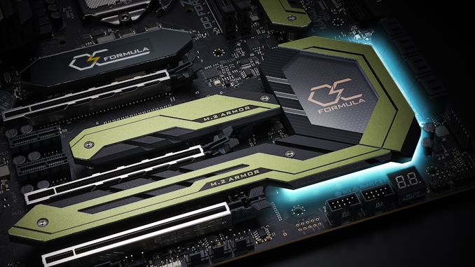
Although the extreme overclocking circle has been getting smaller over the last decade, it is still much alive and resembles an art form. Using more aggressive sub-ambient cooling methods such as dry ice, liquid nitrogen, and in some cases, liquid helium, extreme overclockers have been pushing both Intel and AMD's silicon to its limits for many years. It's been quite a while since ASRock readied up a model capable of competition in the XOC arena. Still, legendary overclocker Nick Shih has helped its engineers design its latest overclocking focused motherboard, the ASRock Z590 OC Formula.
The ASRock Z590 OC Formula drops its recognizable yellow color scheme for an odd green/neon green and black design. Located in the board's center is a new OLED display that can display multiple operating specifications such as voltages, and frequencies, which for overclockers looking for real-time monitoring will find useful.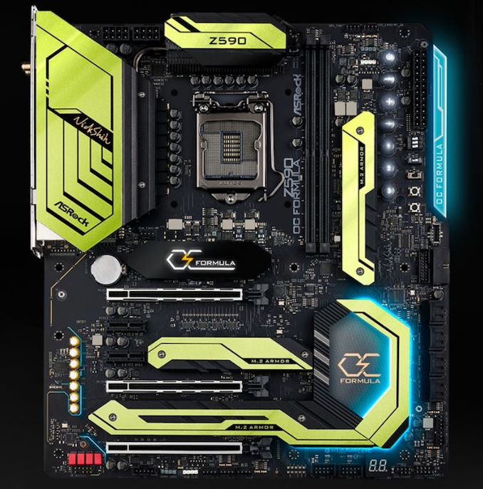
The top-right hand corner is a hardware-based overclockers toolkit that includes DIP switches for enthusiasts looking to disable or enable the board's three full-length PCIe slots. This also includes a slow mode switch, an OC retry button, an LN2 mode switch, a power switch, a reset switch, and on-the-fly frequency adjustment buttons. There are also three numbered buttons that allow direct access to three of Nick Shih's personal overclocking profiles. For extreme tweakers, there are five V-probe voltage monitoring points.
Focusing on the primary specifications, two full-length PCIe 4.0 slots can operate at x16 and x8/x8, a full-length PCIe 3.0 x4 slot, and two PCIe 2.0 x1 slots. For storage, ASRock includes a total of eight SATA ports, six from the chipset with support for RAID 0, 1, 5, and 10 arrays, and two available from an ASMedia SATA controller. Located around the PCIe slot area and forming an L shape around the chipset heatsink are three M.2 slots, with one PCIe 4.0 x4 and two PCIe 3.0 x4/SATA M.2 slots. Other notable elements include a front panel USB 3.2 G2x2 Type-C header, a 5-pin Thunderbolt AIC connector, two USB 3.2 G1 Type-A, and two USB 2.0 headers, as well as a total of eight 4-pin cooling connectors.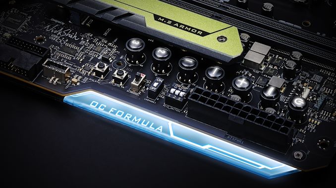
ASRock combines its neon green design with multiple areas of integrated RGB LEDs.
On the rear panel is one USB 3.2 G2 Type-C, three USB 3.2 G2 Type-A, and four USB 3.2 G1 Type-A ports, with two PS/2 ports designed for legacy keyboard and mice; these are a staple of extreme overclocking as USB ports can often stop responding during extreme cooling sessions. Also present are five 3.5 mm LED color-coded audio jacks and S/PDIF optical output driven by a Realtek ALC1220 HD audio codec, as well as a clear CMOS and BIOS Flashback switch. Despite being targeted as an extreme overclocking motherboard, ASRock also includes an Intel I225-V 2.5 GbE and Intel I219-V Gigabit controller pairing, with Intel's latest AX210 Wi-Fi 6E CNVi.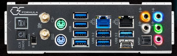
The ASRock Z590 OC Formula looks like a formidable option for pushing Intel's latest 11th generation Rocket Lake processors to the moon and back. Still, it also provides plenty of features for the everyday user. While conventional overclocking focused models of yesteryear have stuck to the basic and core fundamentals designed to deliver the ultimate performance, the Z590 OC Formula balances things out by making it functional with the latest controllers for everyday use too.
ASRock hasn't provided any information about the availability of the Z590 OC Formula or any form of expected pricing.
Gallery: The ASRock Z590 OC Formula Motherboard, Designed For Overclockers


Related Reading- Intel Rocket Lake (14nm) Review: Core i9-11900K, Core i7-11700K, and Core i5-11600K
- The Intel Z590 Motherboard Overview: 50+ Motherboards Detailed
- The Intel B560 Motherboard Overview: 30+ Budget Models Starting From $75
- Intel Launches Rocket Lake 11th Gen Core i9, Core i7, and Core i5
More...
-
04-01-21, 01:09 PM #11076
Anandtech: ASRock Z590 Taichi Review: An Intel Motherboard with Moving Parts (and Thu
Intel has now launched its latest 11th Generation Core processors for desktop. The highest performing of these is the Core i9-11900K, with 8 cores and 16 threads, and it does have some raw core advancements with an updated microarchitecture. These processors need appropriate motehrboards, and although we've seen Intel's Z590 and B560 models already filter into retail channels over the last couple of months, the time is now to start getting to grips with them. The first up for review is the ASRock Z590 Taichi, which currently sits as the brand's flagship model. Some of the Z590 Taichi's main features include dual Thunderbolt 4 Type-C, dual RJ45 including one 2.5 gigabit Ethernet, Intel's latest Wi-Fi 6E CNVi, and comes equipped with a large 14-phase power delivery.
More...
-
04-02-21, 09:19 AM #11077
Anandtech: TSMC to Spend $100B on Fabs and R&D Over Next Three Years: 2nm, Arizona Fa
TSMC this week has announced plans to spend $100 billion on new production facilities as well as R&D over the next three years. The world's largest contract maker of chips says that its fabs are currently working at full load, so to meet demand for its services going forward it will need (much) more capacity. Among TSMC's facilities to go online in the next three to four years are the company's fab in Arizona as well as its first 2nm-capable fab in Taiwan.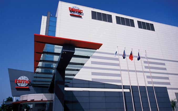
"TSMC is entering a period of higher growth as the multiyear megatrends of 5G and HPC are expected to fuel strong demand for our semiconductor technologies in the next several years," a statement by TSMC with the Taiwan Stock Exchange reads. "In addition, the COVID-19 pandemic also accelerates digitalization in every aspect. In order to keep up with demand, TSMC expects to invest $100 billion over the next three years to increase capacity to support the manufacturing and R&D of advanced semiconductor technologies. TSMC is working closely with our customers to address their needs in a sustainable manner."
$100 Billion to Be Spent on Fabs
TSMC's capital expenditures (CapEx) budget last year was $17.2 billion, whereas its R&D budget was $3.72 billion, or approximately 8.2% of its revenue. This year the company intends to increase its CapEx to somewhere in the range of $25 to $28 billion, which would make for a 45% to 62% year-over-year increase in that spending. The company's R&D spending will also rise as its revenue is expected to grow. In total, TSMC plans to invest around $30 billion or more on CapEx and R&D this year. Taken altogether, if the company intends to spend around $100 billion from 2021 through 2023, its expenditures in the next two years will be roughly flat with 2021, something that should please its investors.
TSMC has a number of important fab projects ahead of it.
- First up, the company needs to build and equip its N5-capable fab in Arizona. The facility will cost around $12 billion, will have a capacity of 20,000 wafer starts per month (WSPM), and will come online in 2024. A recent rumor indicates that TSMC might actually increase capacity of the facility and/or equip it for a more advanced fabrication process, which will increase its cost, but TSMC has never confirmed this information.
- Secondly, TSMC will need to equip its N3-capable fab in Tainan, Taiwan, which is projected to start volume production in the second half of 2022.
- TSMC's third capital-expensive project is the company's N2 (2nm) qualified GigaFab in Hsinchu, Taiwan. Furthermore, TSMC is mulling to build another N2-capable fab in Baoshan, Taiwan. Meanwhile, TSMC still has to complete development of its GAAFET-based N2 node.
- Last but not least, TSMC is set to build two more advanced packaging facilities in Taiwan. The company already has four of such facilities, but it believes that demand for chip stacking and advanced packaging will rise in the future and it will need more capacities. Chip packaging factories are not as expensive as semiconductor production facilities, but they still cost quite a lot.
Recently TSMC wrote a letter to its customers where it explained that its fabs have been fully utilized for about a year now and it still cannot meet rising demand for chips. To that end, the company would have to 'suspend wafer price reductions for a year from the start of 2022,' according to a Bloomberg report.
Competition Intensifying
Right now, TSMC is the world's largest contract maker of chips with no rivals that can match its total production capacity. A some of TSMC's rivals, including GlobalFoundries and UMC, have pulled the plug on development of their leading-edge fabrication processes, so the number of companies that can offer leading-edge nodes has decreased. Yet paradoxically, the competition is also escalating in other respects.
Samsung Semiconductor, which has foundry, DRAM, storage, SoC, and a number of other operations, has been increasing its CapEx investments in the recent years. The company spent $93.2 billion on chip production from 2017 to 2020 and is on track spend another ~$28 billion in 2021, according to IC Insights. Samsung Foundry is still several times smaller than TSMC in terms of sales and capacity, but the gap is closing.
In addition to Samsung Foundry, Intel recently introduced its integrated device manufacturer 2.0 (IDM 2.0) plan that includes offering advanced foundry services and essentially compete against TSMC (while also using its services when needed). Intel has already announced plans to invest $20 billion in two new fabs in Arizona and said it would invest more in expansion of chip production in other parts of the USA as well as in Europe and other parts of the world.
To stay ahead of existing and emerging rivals, TSMC needs to keep investing in R&D and expand its production capacities, so a $100 billion investment plan will be instrumental for these purposes.
More...
-
04-02-21, 01:57 PM #11078
Anandtech: SK Hynix to Build $106 Billion Fab Cluster: 800,000 Wafer Starts a Month
Capping off a busy week for fab-related news, South Korea authorities this week gave SK Hynix a green light to build a new, 120 trillion won ($106.35 billion) fab complex. The fab cluster will be primarily used to build DRAM for PCs, mobile devices, and servers, using process technologies that rely on extreme ultraviolet lithography (EUV). The first fab in the complex will go online in 2025.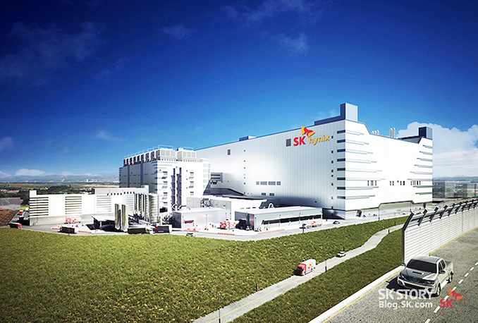
The new cluster will house four huge semiconductor fabrication plants, which will be located on a 4.15 million square-meter site, reports The Korea Herald. The four fabs will have a planned capacity of around 800,000 wafer starts per month (WSPM), which will make the site one of the world's biggest semiconductor production hubs. Keeping in mind that we are dealing with EUV fabs, it is not surprising that a huge 200,000-WSPM plant with EUV tools will cost SK Hynix north of $25 billion. The fab cluster will be located near Yongin, South Korea, 50 kilometers south of Seoul, according to Yonhap news agency that cites the Ministry of Trade, Industry and Energy.
The new fabs will be used to make various types of DRAM using SK Hynix's upcoming production technologies that will use extreme ultraviolet (EUV) lithography. And with a start date still years away, we're likely looking at a fab that will be used to manufacture DDR5, LPDDR5X, and other future types of DRAM.
SK Hynix reportedly plans to start construction of the first fab in the Yongin cluster in the fourth quarter of 2021. Given the expected size of the massive building and the amount of time needed to folly load it with production equipment, SK Hynix expects this first fab to be completed in 2025.
It is necessary to note that just several years ago SK Hynix and Samsung used to build fabs that could produce both DRAM and NAND flash memory – or at least be converted with a minimal amount of effort. This is not the case today as DRAM production now heavily relies on lithography equipment, whereas 3D NAND production uses loads of etching tools, which is why the fabs for different types of memory have to be equipped completely differently.
The fab cluster in Yongin will be SK Hynix's second major DRAM site in South Korea after the company's primary DRAM hub near Icheon that houses its M10, M14, and M16 fabs. The M16 fab was completed in February and will be used for DRAM production using SK Hynix's EUV-based 1a process technology starting the second half of 2021.
More...
-
04-05-21, 06:29 AM #11079
Anandtech: LG Calls it Quits, To Close Mobile Phone Business
This morning, LG issued a press release that announced the board of directors had decided to close down the conglomerate’s mobile phone business. The news is unfortunate, however isn’t too surprising given the mobile division had been accruing continuous operational losses over the last 6 years, greatly denting the company’s financials.
SEOUL, April 5, 2021 — LG Electronics Inc. (LG) announced that it is closing its mobile business unit. The decision was approved by its board of directors earlier today.LG had been one of the major mobile pioneers in the feature phone market, and also a larger player in the early 2010’s with many notable earlier successes such as the LG G2 or the G3.
LG’s strategic decision to exit the incredibly competitive mobile phone sector will enable the company to focus resources in growth areas such as electric vehicle components, connected devices, smart homes, robotics, artificial intelligence and business-to-business solutions, as well as platforms and services.
LG will provide service support and software updates for customers of existing mobile products for a period of time which will vary by region. LG will work collaboratively with suppliers and business partners throughout the closure of the mobile phone business. Details related to employment will be determined at the local level.
Moving forward, LG will continue to leverage its mobile expertise and develop mobility-related technologies such as 6G to help further strengthen competitiveness in other business areas. Core technologies developed during the two decades of LG’s mobile business operations will also be retained and applied to existing and future products.
Unfortunately in the following years, the company had been struck hard by chains of hardware disadvantages, ranging from the Snapdragon 810/808 generation in the G4, a failed attempt at hardware modularity in the G5. LG had also suffered issues over several generations in their OLED display attempts, plagued by lower quality panels with image quality issues, or power efficiency deficits compared to other alternatives in the market who used Samsung Display OLED panels.
At one point, LG had plans to deploy their own in-house design “Nuclun” SoCs into their mobile devices, announcing their partnership with Intel Custom Foundry to produce a leading-edge design on Intel’s 10nm process node. Unfortunately, the project burned to the ground along with Intel’s 10nm struggles, with the chips never seeing the light of day.
LG’s latest device attempts in the form of the V60 and the VELVET were actually greater leaps for the company’s designs as well as executions, however all coming too late, with a continuing problem of availability of the devices, as LG still ran with an availability model of working closely with carriers and releasing devices only in markets where carriers decided they were interested in supporting that device.
The company will be winding down its mobile business through July 31st, refocusing its resources into other divisions of the conglomerate.
More...
-
04-05-21, 11:08 AM #11080
Anandtech: G.Skill Announces DDR4-5333 Memory Kits for Intel Rocket Lake
Designed with a focus on Intel's latest 11th generation Rocket Lake processors and the new memory controller ratios, G.Skill has announced a wave of new memory kits designed to squeeze as much performance out of the platform. The new memory kits for Z590 and Rocket Lake feature speeds of up to DDR4-5333. They will be made available across multiple lines of its range, including the premium Trident Z Royal, Trident Z RGB, and the more affordable Ripjaw V series.
With memory performance and control getting some extra features with Intel's 11th gen desktop, the Z590 chipset with Rocket Lake processors now supports geared memory ratios between the memory controller and the DRAM data rates. The ability of Intel's memory controller in a 1:1 gear ratio can vary, certainly under ambient cooling methods, and not all of Intel's silicon can handle such high frequencies. This is where the gear ratio option becomes beneficial, taking some of the strain off the memory controller and allowing for high frequencies, with G.Skill capitalizing on this with its new memory kits up to DDR4-5333.
The new G.Skill memory kits designed for Intel's Z590 (with Rocket Lake) start from DDR4-4266 with CL19 ratings, with two available capacities: dual-channel 32 GB (2x16) and 64 GB (2x32) kits. Also set to be available include DDR4-4400 kits with CL17 and CL18 latencies, including an operating voltage of 1.50 V in both the 32 GB and 16 GB kits.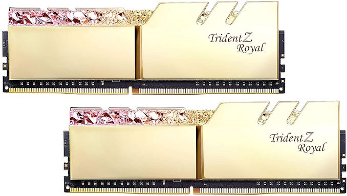
G.Skill's Trident Z Royal DDR4 Memory in Gold
Moving up, there's one kit of DDR4-4600 with CL20 with a total capacity of 64 GB (2 x 32 GB) and three different flavors of DDR4-4800; CL17 and CL18 with 2 x 8 GB kits, and CL20 with 2 x 16 GB. There's one 32 GB (2 x 16 GB) kit at DDR4-5066 with CL19 and an operating voltage of 1.6 V, with one kit maxing out at DDR4-5333 and CL21 latencies, with 2 x 8 GB memory sticks.
G.Skill has announced that its new Rocket Lake and Z590 kits have been validated on the ASUS ROG Strix Z590-E Gaming WIFI, the ASUS ROG Maximus XIII Apex, and MSI's MEG Z590I Unify motherboards with an Intel Core i9-11900K processor. G.Skill also stated that its DDR4-4800 CL17 16 GB (2 x 8 GB) kit uses Samsung B-die memory chips but didn't specify if this was the case across its range.G.Skill Memory For Intel Z590 (Rocket Lake) Rating (MT/s) Latency Voltage Capacity DDR4-4266 19-26-26-46
19-26-26-461.45 V
1.50 V32 GB (2 x 16 GB)
64 GB (2 x 32 GB)DDR4-4400 17-18-18-38
18-24-24-441.50 V
1.50 V32 GB (2 x 16 GB)
16 GB (2 x 8 GB)DDR4-4600 20-30-30-50 1.50 V 64 GB (2 x 32 GB) DDR4-4800 17-19-19-39
19-28-28-48
20-30-30-501.60 V
1.50 V
1.55 V16 GB (2 x 8 GB)
16 GB (2 x 8 GB)
32 GB (2 x 16 GB)DDR4-5066 20-30-30-50 1.60 V 32 GB (2 x 16 GB)
16 GB (2 x 8 GB)DDR4-5333 22-32-32-52 1.60 V 16 GB (2 x 8 GB)
At the time of writing, G.Skill hasn't given us any pricing, but they are expected to launch in Q2 2021. With memory prices set to rise throughout the year, these kits aren't likely to be cheap. The G.Skill Trident Z Royal and Trident Z RGB will likely feature at the higher end of the pricing spectrum, with its Ripjaw Z series sitting as its entry point.
Related Reading- Intel Rocket Lake (14nm) Review: Core i9-11900K, Core i7-11700K, and Core i5-11600K
- DDR5 Memory Specifications Released: Setting the Stage for DDR5-6400 And Beyond
- PNY Unveils XLR8 Gaming Epic-X RGB DDR4-3200 Memory
- GeIL Unveils Orion Series Memory, Up to DDR4-4000 with 32 GB Memory Modules
- TeamGroup Announces Intentions for DDR5, ELITE DDR5-5200 in 2021
More...


 Quote
Quote
Thread Information
Users Browsing this Thread
There are currently 24 users browsing this thread. (0 members and 24 guests)


Bookmarks