

Results 11,191 to 11,200 of 12096
Thread: Anandtech News
-
07-01-21, 09:30 AM #11191
Anandtech: Micron Sells Lehi 3D XPoint Fab to Texas Instruments for $900M
Back in March of this year, Micron announced that it would be getting out of the 3D XPoint business entirely, abandoning the technology and putting its sole 3D XPoint fab up for sale. Now a short few months later, Micron has secured a buyer for the fab – and it’s not Intel. Rather it will be Texas Instruments who picks up the fab, buying it off of Micron for $900 million with plans to convert it over to analog and embedded processors.
The sale of the Lehi fab is the latest and final chapter in Micron’s years-long efforts to unwind its non-volatile memory joint venture with Intel, IM Flash. Over the last decade Micron has acquired Intel’s share of the business in multiple stages, culminating in acquiring the crown jewel of the former partnership, the Lehi, Utah 3D XPoint fab, in 2018. Since then, Micron decided that it would dissolve its 3D XPoint partnership with Intel entirely, culminating with the company abandoning the technology entirely, leaving Micron with a modern fab that it didn’t have an immediate need for.
To that end, Micron put the fab up for sale earlier this year, and has quickly found a buyer amidst the ongoing chip crunch. And while former partner (and current customer) Intel was the most likely candidate, they were not a shoe-in. As our own Billy Tallis put it at the time “Intel is not guaranteed to be the buyer of the Lehi, UT fab. They've doubtless had opportunities to do so before as Intel and Micron unwound their partnership”.
Instead, the memory fab will be going to Texas Instruments, who is buying the building – but not all of the tools. Though designed for 3D XPoint production, the Lehi fab is otherwise a modern, 2 million square foot fab that can process 300mm wafers and is readily capable of being converted to other uses; and this is the direction TI will be taking things. The company is currently planning to equip the fab for the production of analog and embedded processors on the 65nm and 45nm nodes, with the ability to take the fab “beyond those nodes as required.” For Texas Instruments this will be their fourth 300mm fab.
Meanwhile the remaining memory tools that TI isn’t buying will be further assets for Micron, who will be keeping some of them and selling the rest. According to the company’s press release, some of these tools are getting redeployed to other Micron fabs, some have been sold, and yet other tools are still up for sale. Micron doesn’t mention who the tool buyers are, but given the specialized nature of the equipment, it wouldn’t be too surprising if Intel were among them. Overall, Micron is valuing the tools at $600 million, bringing the total value of the transaction to a cool $1.5 billion.
The sale is expected to close at the end of the year, at which point TI will be putting out offers to retain all of the Lehi staff as the fab gets converted over to TI’s analog and logic processes.
Finally, for the sole company to actually use 3D XPoint memory, the sale of the Lehi fab calls into question Intel’s own 3D XPoint production plans. Having sold their share of the fab to Micron, Intel transitioned to being a customer of the world’s only 3D XPoint fab in late 2019 – an arrangement that left the fab operating in the red for Micron, as Intel’s 3D XPoint orders weren’t enough to fully utilize the fab. IM Flash jointly developed Intel’s current (second-generation) 3D XPoint memory technology as well, and it’s believed that the Lehi fab has been producing all of that memory for Intel.
So it remains to be seen just how Intel will be impacted, as the sale puts a running clock on how much longer they can buy 3D XPoint memory from the third-party fab. Eventually Intel will need to setup their own fab – likely in Rio Rancho, NM, where their 3D XPoint R&D takes place – but so far the company hasn’t announced any such plans.
Sources: Texas Instruments, Micron
More...
-
07-02-21, 09:02 AM #11192
Anandtech: ASUS Launches Zenfone 8 in US: Starting at $599
Following the phone’s initial announcement mid-May, this week ASUS has officially launched their new ZenFone 8 in the US starting at a price of $599. The ZenFone 8 is a bit unusual in the market as it is trying to fit itself in the niche of a small flagship device – at least in terms of performance.
More...
-
07-02-21, 10:50 AM #11193
Anandtech: Cristiano Amon Takes over as Qualcomm CEO: Reiterates Focus on Custom CPUs
As of June 30th, Qualcomm’s Cristiano Amon has taken over as the company’s CEO, replacing his predecessor Steve Mollenkopf which has now retired. In statements to Reuters, Amon had made comments regarding the company’s future CPU roadmap, which come to further contextualise the company’s completed acquisition of NUVIA last March.
More...
-
07-06-21, 05:37 AM #11194
Anandtech: Examining OnePlus' Performance Behaviour: Optimization or Misrepresentatio
We've discovered weird behaviour on the OnePlus 9 Pro flagship: Popular apps are performance limited, while benchmarks are unaffected. Is this battery optimisation, or misrepresentation of the user experience?
More...
-
07-07-21, 03:57 AM #11195
Anandtech: Intel Hybrid CPU Starts 'End of Life' Process
As I opened my inbox this morning, I was surprised. I keep track of when Intel puts products on End of Life (or starts the process through something called Product Discontinuance), and so I usually see a run of 3-5 year old CPUs or storage or servers pass through without much of a worry. When I opened up my daily brief today however, the headline read ‘Core Processor with Hybrid Technology Discontinued’, which immediately struck me as a bit crazy.
Intel announced Lakefield, its only Hybrid CPU on the market, in January 2019. It pairs one of its big cores with four smaller Atom cores in a small 12mm square package. Not only this, Lakefield is one of Intel’s first Foveros packaging processors, with a 10nm compute piece of silicon sitting on top of an IO die, all packaged together with DRAM on top. The goal of the Lakefield design was to produce a processor with a super low idle power, but also have enough performance for hand-held devices. Intel quoted 1.2 mW when in idle, meeting that goal.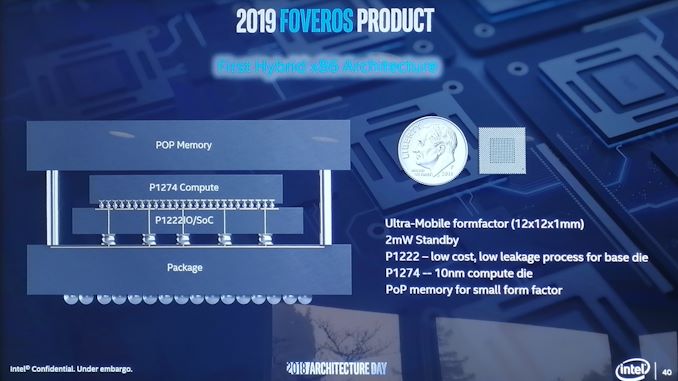
Lakefield came to market in June 2020 in two products: the Samsung Galaxy Book S 13.3-inch clamshell laptop, and the Lenovo ThinkPad X1 Fold, a foldable display-based design. Both of these products were premium priced, particularly the Fold with its display, however reported performance was more akin to a quad-core Atom notebook than the $2000 quad-core mobile devices they were aiming for. Battery life sounded good, although we have never tested it at AnandTech due to lack of access to review samples from Samsung, Lenovo, or Intel.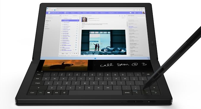
The key thing was the Hybrid CPU design. By pairing one of Intel’s big cores with four of its smaller Tremont Atom cores, the goal was to run the device almost exclusively on the Atom cores for efficiency and then call on the big core when anything latency related was required, such as when the user touches the screen or the keyboard. Within 16 milliseconds (or one frame at 60 Hz), the processor would switch over to the big core for the touch screen interaction, do what it needed to do (often in under 16 ms), and then power back down.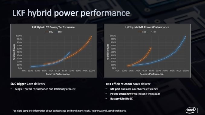
In principle, the concept is sound and makes a lot of sense, especially if the goal is to save battery. As Intel’s first Hybrid CPU design however, there were some initial teething issues as managing threads between the different performance levels required adjustments to Windows’ scheduler. Microsoft already has experience with this when dealing with Windows on Snapdragon devices using the Arm architecture, however it was a first for x86 and the first implementations were reportedly quite rough.
In reality, because of the price of the device, it was compared to hardware that had only big cores. Even if it was compared to Atom based notebooks in the $400 range, because the processor was a low powered device, often lower than the Atom notebooks it was being compared to, it didn’t fall favorably in those benchmarks either. The goal of Lakefield for Intel wasn’t performance, but experience and form factor innovation, which benchmarks never indicate.
The note today from Intel indicates that Lakefield is now on the path to End of Life. This means the following milestones:
- Start of Product Discontinuance: July 6th 2021
- Last Corporate Assurance: October 8th 2021
- Last Product Discontinuance Order: October 22nd 2021
- Orders are Non-Cancellable from October 22nd 2021
- Last Shipment Date: April 29th 2022
The start of the process means announcing that they will stop manufacturing processors (July 6th) and if a company wants to put in an order, they have until October 22nd. However that’s also the date where orders can’t be canceled or returned, and all orders will be shipped by April 29th. That means that products could still come out with Lakefield after April 29th, however the OEM partners will not have any means to secure additional stock.
Intel has set its sights on its future Hybrid CPU designs, with the upcoming Alder Lake platform set to launch end of this year in either desktops or notebooks. There is also talk that Windows 11 is better suited to deal with Intel’s hybrid designs from a scheduler perspective. Overall, to see its only public Hybrid CPU suddenly go on product discontinuance after only a year in the market isn’t a great commitment to the technology from OEM partners. Intel's own Product Change Notification states that 'market demand for the products listed has shifted to other Intel products'.
Related Reading- The Intel Lakefield Deep Dive: Everything To Know About the First x86 Hybrid CPU
- Intel Discloses Lakefield CPUs Specifications: 64 Execution Units, up to 3.0 GHz, 7 W
- Samsung Unveils Intel-based Galaxy Book S: Intel’s Lakefield Inbound
- Lenovo’s ThinkPad X1 Fold: Combining Foldable Displays, 5G and Lakefield into a… Laptop?
- Intel: Lakefield in 2020, Possible 5G on Foveros
- Intel's new Atom Microarchitecture: The Tremont Core in Lakefield
- Hot Chips 31 Live Blogs: Intel Lakefield and Foveros
- CES 2019 Quick Bytes: Intel’s 10nm Hybrid x86 Foveros Chip is Called Lakefield
Gallery: Intel Hybrid CPU Starts 'End of Life' Process

_carousel_thumb.jpg)


More...
-
07-07-21, 03:57 AM #11196
Anandtech: Intel Continues to Rehire Veterans: At Some Point Theyll Run Out
News on the wire today is that Intel has rehired 28-year veteran Shlomit Weiss into the position of Senior VP and Co-General Manager of Intel’s Design Engineering Group (DEG), a position recently vacated by Uri Frank who left to head up Google’s SoC development. As reported in Tom’s Hardware and confirmed in her own LinkedIn announcement, Weiss will be working at Intel’s Israel design center alongside Sunil Shenoy and is ‘committed to ensure that the company continues to lead in developing chips’. Weiss is the latest in an ever growing list of ‘re-hiring’ Intel veterans, which leads to the problem that at some point Intel will run out of ex-employees to rehire and instead nurture internal talent for those roles.
More...
-
07-08-21, 10:42 AM #11197
Anandtech: ASUS Announces "Smartphone for Snapdragon Insiders" - A Real Product, or J
Today ASUS and Qualcomm are announcing the “Smartphone for Snapdragon Insiders” - a ASUS designed phone with extensive Snapdragon branding – a ROG Phone 5 spin-off, or just a pointless marketing exercise?
More...
-
07-09-21, 01:20 PM #11198
Anandtech: Samsung: Deployment of 3nm GAE Node on Track for 2022
Samsung Foundry has made some changes to its plans concerning its 3 nm-class process technologies that use gate-all-around (GAA) transistors, or what Samsung calls its multi-bridge channel field-effect transistors (MBCFETs). Based on new information direct from Samsung, it would appear that its first version of 3nm, 3GAE (3nm gate-all-around early), is coming to high volume manufacturing a year later than expected, but also it seems to have removed this technology from its public roadmap, suggesting it may be for internal use only.
Meanwhile, 3GAE's successor 3GAP (3nm gate-all-around plus) node is still in the roadmap, it is on track for volume manufacturing in 2023.
3GAE on Track for 2022, Maybe Just Not for Everyone
At its recent Foundry Forum 2021 in China, Samsung Foundry presented its updated public technology roadmap which was then republished by bloggers at Baidu and Weibo.
On its FinFET technologies, both 5LPP and 4LPP nodes are new to the roadmap, and set for high-volume manufacturing (HVM) in 2021 and 2022, respectively.
For GAA technology, 3GAE is absent from the roadmap, but 3GAP is there. We reached out to Samsung and a representative confirmed that the 3GAE technology is still on track for ramp in 2022. From the slide, we can see that MBCFET-based 3GAP will enter its HVM phase sometime in 2023.
"As for the 3GAE process, we've been in discussion with customers and expect to mass-produce 3GAE in 2022," the spokesperson said.
The absence of 3GAE process from the public roadmap may be explained by the fact that it will only be available to Samsung's own LSI division, just like some other (E)arly nodes. That being said, previous generation (E)arly nodes are still mentioned in the slides that the company demonstrated.
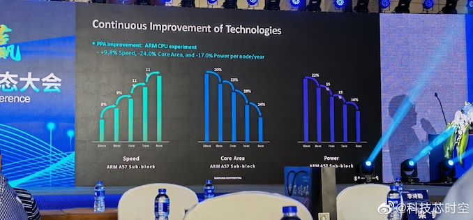
Samsung originally announced its MBCFET-based 3GAE and 3GAP nodes in May 2019. Back then, the company promised a 35% performance increase, a 50% power consumption reduction, and a 45% area reduction for 3GAE compared to 7LPP. Furthermore, the company announced the availability of v0.1 of its 3nm PDK and at the time said that volume production using 3GAE was set to start in late 2021. With that moving to 2022 based on the latest information, one might interpret this as either a delay or miscalculation based on enabling GAA designs at scale.
However on the plus side, Samsung taped out the first 3 nm test chip several weeks ago. It also announced the availability of Synopsys EDA tools compatible with the new fabrication technologies. The use of fabrication processes that rely on brand-new transistors is always a challenge - in addition to new electronic design automation (EDA) tools, chip developers need all-new IP. We look forward to hearing more disclosures on that front.
A New 4LPP Node on FinFETs
While it looks like general customers are not going to use Samsung's 3 nm nodes until 2023, the newly announced 4LPP is set to meet the requirements of the company's clients in 2022. Since 4LPP relies on familiar FinFETs, it will be much easier for Samsung's customers to use this node when compared to any 3nm GAA nodes early in their lifecycle.
It is noteworthy that Samsung now considers its 5 nm and 4 nm-class technologies as different node branches on its slides. Previously, the foundry considered its 4LPE as an evolution of its 7LPP process. Perhaps this is because 4 nm is set to offer very tangible PPAc (power, performance, area, cost) advantages over 5 nm, or because there are substantial internal changes (e.g., new materials, significantly higher usage of extreme ultraviolet lithography, etc.).
For example, one of Samsung's slides specifically mentions density and performance improvements for 5LPE and 5LPP, but only mentions power and performance improvements for 4LPP. The overlapping technologies will also help to mitigate risks if one of the nodes does not meet certain expectations.
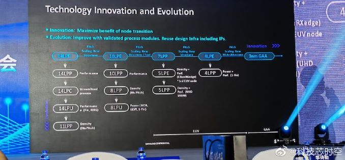
Surprisingly, Samsung Foundry is set to ramp production using its 4LPE and 5LPP technologies at around the same time in 2021, which could enable it to offer different PPAc advantages for different chip designs.
Summary
While Samsung Foundry's GAAFET/MBCFET 3 nm plans appear to have changed and slipped by a year, it is unlikely a big problem for the company as its (E)arly nodes were never widely adopted. To cover that additional year, the company's new 5LPP and 4LPP FinFET-based technologies are set to enable PPA advantages for Samsung Foundry's clients and enable the company to gain more experience with EUV equipment before using it for its 3GAE/3GAP nodes.
More...
-
07-09-21, 01:20 PM #11199
Anandtech: ASUS ROG Maximus XIII Hero Review: Everything for Rocket Lake
On our test bench today is one of ASUS ROG's enthusiast models designed for Intel's Rocket Lake processors. The ASUS ROG Maximus XIII Hero brings plenty of premium controllers and connectivity to the table including dual 2.5 GbE, dual Thunderbolt 4 Type-C, Wi-Fi 6E, four M.2 slots, and a robust 14-phase power delivery capable of pushing Rocket Lake above its capabilities. We have put the Z590 Hero through its paces to see if it is the champion model in the sub $500 Z590 market.
More...
-
07-12-21, 02:00 PM #11200
Anandtech: Intel Accelerated Webcast on July 26th: Update on Process Technology and R
Earlier this year, new Intel CEO Pat Gelsinger outlined his new ‘IDM 2.0’ vision for Intel. This vision was a three pronged strategy based on improving its own process node technology, mixing in other foundry technology where needed, and also realigning its manufacturing for a new foundry service offering allowing other semiconductor companies to use Intel’s manufacturing expertise. As part of the journey towards Gelsinger’s IDM 2.0 vision, we were told to expect updates at a more regular cadence, and the announcement of ‘Intel Accelerated’ in a couple of weeks is the next event on the calendar._575px.jpg)
More...


 Quote
QuoteThread Information
Users Browsing this Thread
There are currently 44 users browsing this thread. (0 members and 44 guests)


Bookmarks