

Results 11,311 to 11,320 of 12091
Thread: Anandtech News
-
10-13-21, 09:41 AM #11311
Anandtech: AMD Launches Radeon RX 6600: More Mainstream Gaming For $329
AMD this morning is once again expanding its Radeon RX 6000 family of video cards, this time with the addition of a second, cheaper mainstream offering: the Radeon RX 6600. Being announced and launched this morning, the Radeon RX 6600 is aimed at the mainstream 1080p gaming market, taking its place as a second, cheaper alternative to AMD’s already-released Radeon RX 6600 XT. Based on the same Navi 23 GPU as its sibling, the Radeon RX 6600 comes with 28 CUs’ worth of graphics hardware, 8GB of GDDR6 VRAM, and a 32MB Infinity Cache, with prices starting at $329.
More...
-
10-14-21, 10:33 AM #11312
Anandtech: The Be Quiet! Pure Loop 280mm AIO Cooler Review: Quiet Without Compromise
Today we're taking our first look at German manufacturer Be Quiet's all-in-one (AIO) CPU liquid coolers, with a review of their Pure Loop 280mm cooler. True to their design ethos, Be Quiet! has built the Pure Loop to operate with as little noise as is reasonably possible, making for a record-quiet cooler that also hits a great balance between overall performance, an elegant appearance, and price.
More...
-
10-15-21, 11:00 AM #11313
Anandtech: G.Skill Unveils Premium Trident Z5 and Z5 RGB DDR5 Memory, Up To DDR5-6400
With memory manufacturers clamoring over themselves to push out DDR5 in time for the upcoming launch of Intel's Alder Lake processors, G.Skill has unveiled its latest premium Trident Z5 kits. The latest Trident kits are based on Samsung's new DDR5 memory chips and range in speed from DDR5-5600 to DDR5-6400, with latencies of either CL36 or CL40. Meanwhile, G.Skill has also opted to use this opportunity to undertake a complete design overhaul from its previous DDR4 memory, with a fresh new look and plenty of integrated RGB, and is .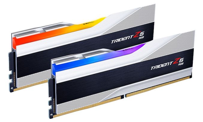
Looking at performance, the top SKU comes with fast speeds of DDR5-6400, with either a latency of CL 36-36-36-76 or CL 40-40-40-76. Both the lower-rated kits of DDR5-6000 and DDR5-5600 are available with the same latencies, while all of the six combinations will be available in 32 GB kits, with 2 x 16 GB memory modules. The new G.Skill Trident Z5 and Z5 RGB memory kits will also feature the latest Samsung memory ICs, with G.Skill hand screening the memory chips themselves to ensure maximum stability and performance.G.Skill Trident Z5 DDR5 Memory Specifications Speed Latencies Voltage Capacity DDR5-6400 36-36-36-76
40-40-40-76??? 32 GB (2 x 16 GB) DDR5-6000 36-36-36-7640-40-40-76??? 32 GB (2 x 16 GB)DDR5-5600 36-36-36-7640-40-40-76??? 32 GB (2 x 16 GB)
At the time of writing, G.Skill hasn't confirmed the operating voltages of each kit. G.Skill also hasn't unveiled its pricing at this time, but it did say that the Trident Z5 and Trident Z5 RGB kits will be available from November.
Meanwhile in terms of aesthetics, the G.Skill Trident Z5 DDR5 memory features a new design compared with previous Trident Z series kits. The Trident Z5 comes with a new dual texture heat spreader design and is available either with a black top bar (Z5) or a new translucent RGB light bar (Z5 RGB). It's also available in black and silver, with a black brushed aluminum insert across both colors, making it stand out.
With the RGB enabled G.Skill Trident Z5 RGB DDR5 memory kits, the lighting can be customized via its Trident Z lighting control software or synced with other third-party software supplied by vendors such as ASRock, ASUS, GIGABYTE, and MSI's own RGB software.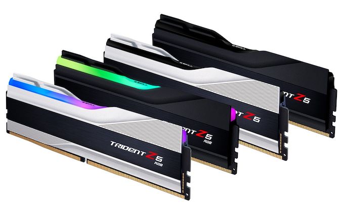
Gallery: G.Skill


Related Reading- Samsung Teases 512 GB DDR5-7200 Modules
- Insights into DDR5 Sub-timings and Latencies
- Computex 2021: TeamGroup Announces its First DDR5-4800 Memory Module
- TeamGroup Announces Intentions for DDR5, ELITE DDR5-5200 in 2021
More...
-
10-15-21, 11:00 AM #11314
Anandtech: The EVGA Z590 Dark Motherboard Review: For Extreme Enthusiasts
Getting the most out of Intel's Core i9-11900K primarily relies on two main factors: premium cooling for the chip itself, and a solid motherboard acting as the foundation. And while motherboard manufacturers such as EVGA can't do anything about the former, they have quite a bit of experience with the latter.
Today we're taking a look at EVGA's Z590 Dark motherboard, which is putting EVGA's experience to the test as one of a small handful of LGA1200 motherboards geared for extreme overclocking. A niche market within a niche market, few people really have the need (or the means) to overclock a processor within an inch of its life. But for those that do, EVGA has developed a well-earned reputation with its Dark series boards for pulling out all of the stops in helping overclockers get the most out of their chips. And even for the rest of us who will never see a Rocket Lake chip pass 6GHz, it's interesting to see just what it takes with regards to motherboard design and construction to get the job done.
More...
-
10-15-21, 04:38 PM #11315
Anandtech: TSMC to Build Japan's Most Advanced Semiconductor Fab
Fabs are well-known for being an expensive business to be in, so any time a new fab is slated for construction, it tends to be a big deal – especially amidst the current chip crunch. To that end, TSMC this week has announced plans to build a new, semi-specialized fab in Japan to meet the needs of its local customers. The semiconductor manufacturing facility will focus on mature and specialty fabrication technologies that are used to make chips with long lifecycles for automakers and consumer electronics. The fab will be Japan's most advanced fab for logic when it becomes operational in late 2024 and if the rumors about planned investments are correct, it could also be Japan's largest fab for logic chips.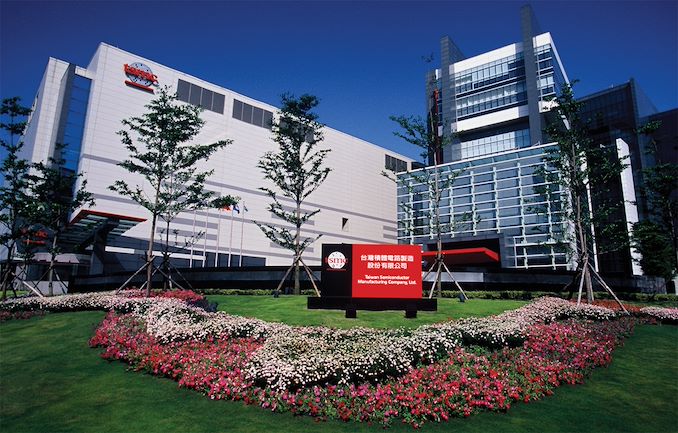
"After conducting due diligence, we announce our intention to build a specialty technology fab in Japan, subject to our board of directors approval," announced CC Wei, chief executive officer of TSMC, during a conference call with investors and financial analysts. "We have received a strong commitment to support this project from both our customers and the Japanese government."
Comes Online in Late 2024
TSMC's fab in Japan will process 300-mm wafers using a variety of specialty and mature nodes, including a number of 28 nm technologies as well as 22ULP process for ultra-low-power devices. These nodes are not used to make leading-edge ASICs and SoCs, but they are widely used by automotive and consumer electronics industries and will continue to be used for years to come not only for existing chips, but for upcoming solutions as well.
"This fab will utilize 20 nm to 28 nm technology for semiconductor wafer fabrication," Wei added. "Fab construction is scheduled to begin in 2022 and production is targeted to begin in late 2024, further details will be provided subject to the board approval."
While TSMC disclosed the specialized nature of the fab, its schedule, and the fact that it gained support from clients and the Japanese government, the company is not revealing anything beyond that. In fact, while it confirmed that the cost of the semiconductor production facility is not included in its $100 billion three-year CapEx plan, it refused to give any estimates about its planned investments in the project.
Meanwhile, there are many things that make this fab special for TSMC, Japan, and the industry.
The Most Advanced Logic Fab in Japan
It was late 2005, AMD and Intel started to ship their first dual-core processors and the CPU frequency battle was officially over. Intel was getting ready to introduce its first 65nm chips in early 2006 and all of a sudden Panasonic said that it had started volume production of the world's first application processors using a 65 nm technology, which it co-developed with Renesas, putting Panasonic a couple of months ahead of mighty Intel. In mid-2007, Panasonic again beat Intel to punch by several months with its 45 nm fabrication process.
But with their 32 nm node, Panasonic was 9 – 10 months behind Intel. And while the company did a half-node shrink of this process, it ultimately pulled the plug on 22nm following other Japanese conglomerates that opted out from the process technology race even earlier. By now, all Japanese automotive and electronics companies outsource their advanced chips to foundries, who in turn, build the majority of them outside of Japan.
By bringing a 22ULP/28nm-capable fab to Japan, TSMC's plans will not only brings advanced logic manufacturing back to the country, but it would also amount to the most advanced fab in Japan. TSMC is also constructing an R&D center in Japan and cooperates with the University of Tokyo on various matters, so its presence in the country is growing, which is good news for the local semiconductor industry.
Previously TSMC concentrated its fabs and R&D facilities in Taiwan, but it looks like its rapid growth fueled by surging demand for semiconductors as well as geopolitical matters are compelling the foundry to diversify its production and R&D locations.
What is particularly interesting is that according to a Nikkei report, the Japanese production facility will be co-funded by TSMC, the Japanese government, and Sony. This marks another major strategy shift for TSMC, which tends to fully own its fabs. In fact, if the Nikkei report is to be believed, the whole project will cost around $7 billion (though it is not said whether this is the cost of first phase of the fab, or a potential multi-year investment).
To put the number into context, SMIC recently announced plans to spend around $8.87 billion on a fab with planned capacity of around 100,000 300-mm wafer starts per month (WSPM). TSMC's facility will presumably cost less and will be built in a country with higher operating costs, so it may well not be a GigaFab-level facility (which have capacity of ~100K WSPM). But still, we are talking about a sizable fab that could have a capacity of tens of thousands of wafer starts per month, which would make it Japan's biggest 300-mm logic facility ever. Just for comparison, the former Panasonic fab in Uozo (now controlled by Tower Semiconductor and Nuvoton) has a capacity of around 8,000 WSPM.
TSMC has not formally confirmed any numbers about its Japanese fab, but the company tends to build rather large production facilities that can be expanded if needed. Meanwhile, a fab in Japan that well serve needs of local automotive and electronics conglomerates promises to help them to avoid shortages of chips in the future. This would also leave TSMC free to assign its 28nmTaiwanese and Chinese production lines to other applications, including PCs, which is important for the whole industry.
More...
-
10-18-21, 11:42 AM #11316
Anandtech: The Apple 2021 Fall Mac Event Live Blog 10am PT (17:00 UTC)
Following last month’s announcement event of Apple’s newest iPhone and iPad line-ups, today we’re seeing Apple hold its second fall event, where we expect the company to talk about all new things Mac. Last year’s event was a historic one, with Apple introducing the M1 chip and new powered Mac devices, marking the company’s move away from x86 chips from Intel, taking instead their own future in their hands with their own custom Arm silicon. This year, we’re expecting more chips and more devices, with even more performance to be release. Stay tuned as we cover tonight’s show.
More...
-
10-18-21, 11:42 AM #11317
Anandtech: TSMC Roadmap Update: 3nm in Q1 2023, 3nm Enhanced in 2024, 2nm in 2025
TSMC has introduced a brand-new manufacturing technology roughly every two years over the past decade. Yet as the complexity of developing new fabrication processes is compounding, it is getting increasingly difficult to maintain such a cadence. The company has previously acknowledged that it will start producing chips using its N3 (3 nm) node about four months later than the industry is used to (i.e., Q2), and in a recent conference call with analysts, TSMC revealed additional details about its latest process technology roadmap, focusing on their N3, N3E, and N2 (2 nm) technologies.
N3 in 2023
TSMC's N3 technology will provide full node scaling compared to N5, so its adopters will get all performance (10% - 15%), power (-25% ~ -30%), and area (1.7x higher for logic) enhancements that they come to expect from a new node in this day and age. But these advantages will come at a cost. The fabrication process will rely extensively on extreme ultraviolet (EUV) lithography, and while the exact number of EUV layers is unknown, it will be a greater number of layers than the 14 used in N5. The extreme complexity of the technology will further add to the number of process steps – bringing it toto well over 1000 – which will further increase cycle times.
As a result, while mass production of the first chips using TSMC's N3 node will begin in the second half of 2022, the company will only be shipping them to an undisclosed client for revenue in the first quarter of 2023. Many observers, however, expected these chips to ship in late 2022.
"N3 risk production is scheduled in 2021, and production will start in second half of 2022," said C.C. Wei, CEO of TSMC. "So second half of 2022 will be our mass production, but you can expect that revenue will be seen in first quarter of 2023 because it takes long — it takes cycle time to have all those wafer out."
N3E in 2024
Traditionally, TSMC offers performance-enhanced and application-specific process technologies based on its leading-edge nodes several quarters after their introduction. With N3, the company will be changing their tactics somewhat, and will introduce a node called N3E, which can be considered as an enhanced version of N3.
This process node will introduce an improved process window with performance, power, and yield enhancements. It is unclear whether N3 meets TSMC's expectations for PPA and yield, but the very fact that the foundry is talking about improving yields indicates that there is a way to improve it beyond traditional yield boosting methods.
"We also introduced N3E as an extension of our N3 family," said Wei. "N3E will feature improved manufacturing process window with better performance, power and yield. Volume production of N3E is scheduled for one year after N3."
TSMC has not commented on whether N3E will be compatible with N3's design rules, design infrastructure, and IPs. Meanwhile, since N3E will serve customers a year after N3 (i.e., in 2024), there will be quite some time for chip designers to prepare for the new node.
N2 in 2025
TSMC's N2 fabrication process has largely been a mystery so far. The company has confirmed that it was considering gate-all-around field-effect transistors (GAAFETs) for this node, but has never said that the decision was final. Furthermore, it has never previously disclosed a schedule for N2.
But as N2 gets closer, TSMC is slowly locking down some additional details. Particularly, the company is now formally confirming that the N2 node is scheduled for 2025. Though they are not elaborating on whether this means HVM in 2025, or shipments in 2025.
"I can share with you that in our 2-nm technology, the density and performance, will be the most competitive in 2025," said Wei.
More...
-
10-18-21, 08:31 PM #11318
Anandtech: Apple Announces M1 Pro & M1 Max: Giant New Arm SoCs with All-Out Performan
Today’s Apple Mac keynote has been very eventful, with the company announcing a new line-up of MacBook Pro devices, powered by two different new SoCs in Apple’s Silicon line-up: the new M1 Pro and the M1 Max.
The M1 Pro and Max both follow-up on last year’s M1, Apple’s first generation Mac silicon that ushered in the beginning of Apple’s journey to replace x86 based chips with their own in-house designs. The M1 had been widely successful for Apple, showcasing fantastic performance at never-before-seen power efficiency in the laptop market. Although the M1 was fast, it was still a somewhat smaller SoC – still powering devices such as the iPad Pro line-up, and a corresponding lower TDP, naturally still losing out to larger more power-hungry chips from the competition.
Today’s two new chips look to change that situation, with Apple going all-out for performance, with more CPU cores, more GPU cores, much more silicon investment, and Apple now also increasing their power budget far past anything they’ve ever done in the smartphone or tablet space.
More...
-
10-19-21, 11:30 AM #11319
Anandtech: The Arm DevSummit 2021 Keynote Live Blog: 8am PT (15:00 UTC)
This week seems to be Arm's week across the tech industry. Following yesterday's Arm SoC announcements from Apple, today sees Arm kick off their 2021 developer's summit, aptly named DevSummit. As always, the show is opening up with a keynote being delivered by Arm CEO Simon Segars, who will be using the opportunity to lay out Arm's vision of the future.
Arm chips are already in everything from toasters to PCs – and Arm isn't stopping there. So be sure to join us at 8am PT (15:00 UTC) for our live blog coverage of Arm's keynote.
More...
-
10-19-21, 06:20 PM #11320
Anandtech: Google Announces Pixel 6, Pixel 6 Pro: The New Real Flagship Pixels
Today, after many weeks, even months of leaks and teasers, Google has finally announced the new Pixel 6 and Pixel 6 Pro – their new flagship line-up of phones for 2021 and carrying them over into next year. The two phones had been teased quite on numerous occasions and have probably one of the worst leak records of any phone ever, and today’s event revealed little unknowns, but yet still Google manages to put on the table a pair of very interesting phones, if not, the most interesting Pixel phones the company has ever managed to release.
More...


 Quote
QuoteThread Information
Users Browsing this Thread
There are currently 23 users browsing this thread. (0 members and 23 guests)


Bookmarks