

Results 11,361 to 11,370 of 12094
Thread: Anandtech News
-
12-01-21, 05:16 PM #11361
Anandtech: Qualcomm Snapdragon Tech Summit: Day 2 Keynote on ACPC and Gaming
We're here on Day 2 of the Qualcomm Snapdragon Tech Summit, ready for a keynote on the next generation of Always Connected PCs (ACPCs) and non-Smartphone gaming. We've got new silicon and new handheld devices to talk about.
More...
-
12-02-21, 11:09 AM #11362
Anandtech: Seagate Exos X20 and IronWolf Pro 20TB Expand Retail 20TB HDD Options
Seagate has updated their flagship capacity options for the retail HDD market with the availability announcement for two new hard drives today - the Exos X20 and IronWolf Pro 20TB. These two models join the recently-released Western Digital WD Gold 20TB and Ultrastar HC560 to round out the 20TB hard drives currently available for retail purchase.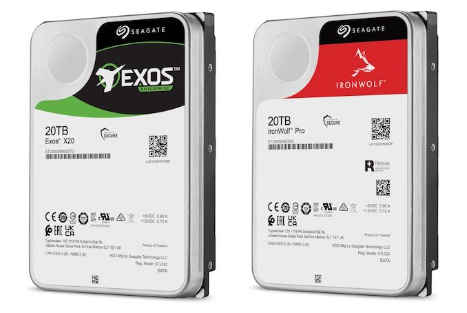
The Exos X20 comes with SATA as well as SAS 12Gbps interface options, and includes SED (self-encrypting drive) models while the IronWolf Pro is SATA-only (similar to previous generations). The Exos X20 has a workload rating of 550 TB/yr, while the IronWolf Pro version is rated for 300 TB/yr. A detailed comparative summary of the different specifications of the two new drives and how they stack up against the Western Digital offerings is provided in the table below. Only the SATA options of the Exos X20 and the Ultrastar HC560 are being considered for this purpose. The two model numbers corresponding to these are for the SED and non-SED (standard) options.
The IronWolf Pro model also has a 1W standby / sleep-mode power consumption rating that could prove useful in NAS units that are subject to constant 24x7 traffic. The idle acoustics are at the higher end for the Seagate models, but the seek numbers make up for it. Unfortunately, we do not have a way to compare the power consumption numbers based on the datasheets, as the workloads used for the characterization are different between the two vendors. That said, the idle numbers lean again towards the Seagate models.2021 Retail 20TB HDDs - Comparative Specifications Seagate
Exos X20 20TBSeagate
IronWolf Pro 20TBWestern Digital
WD Gold 20TBWestern Digital
Ultrastar HC560Model ST20000NM007D
ST20000NM000D (SED)ST20000NE000 WD201KRYZ WUH722020ALE6L1 (SED)
WUH722020ALE6L4Recording Technology Conventional Magnetic Recording
(CMR)Conventional Magnetic Recording with Energy-Assist
(CMR / EAMR)RPM 7200 RPM DRAM Cache 256 MB 512 MB Helium-Filling Yes Sequential Data Transfer Rate
(MBps)285 MB/s 269 MB/s MTBF 2.5 M 1.2 M 2.5 M Rated Annual Workload 550 TB 300 TB 550 TB Acoustics Idle 28 dB 20 dB Seek 30 dB 32 dB 36 dB Power Consumption Random read/write 9.4 W / 8.9 W (100R/100W @ QD16) 9.4 W / 8.9 W (100R/100W @ QD16) 7 W
(50R/50W @ QD1)Idle 5.5 W 5.4 W 6 W Warranty 5 Years 5 Years
(3 years DRS)5 Years Pricing $670 $650 $680 $700
It must be noted here that the list price premium for the WD models can be accounted for by the use of OptiNAND technology in the WD Gold and Ultrastar HC560. We reached out to Seagate on the use of HAMR in the new models, and surprisingly, Seagate indicated that the two new hard drives being introduced to retail today do not use heat-assisted magnetic recording.
More...
-
12-02-21, 09:10 PM #11363
Anandtech: United States FTC Files Lawsuit to Block NVIDIA-Arm Acquisition
In the biggest roadblock yet to NVIDIA’s proposed acquisition of Arm, the United States Federal Trade Commission (FTC) has announced this afternoon that the regulatory body will be suing to block the merger. Citing concerns over the deal “stifling the innovation pipeline for next-generation technologies”, the FTC is moving to scuttle the $40 billion deal in order to protect the interests of the wider marketplace.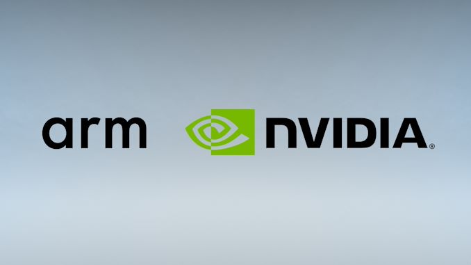
The deal with current Arm owner SoftBank was first announced in September of 2020, where at the time SoftBank had been shopping Arm around in an effort to either sell or spin-off the technology IP company. And while NVIDIA entered into the deal with bullish optimism about being able to close it without too much trouble, the company has since encountered greater political headwinds than expected due to the broad industry and regulatory discomfort with a single chip maker owning an IP supplier used by hundreds of other chip makers. The FTC, in turn, is the latest and most powerful regulatory body to move to investigate the deal – voting 4-0 to file the suit – following the European Union opening a probe into the merger earlier this fall. The
While the full FTC complaint has yet to be released, per a press release put out by the agency earlier today, the crux of the FTC’s concerns revolve around the advantage over other chip makers that NVIDIA would gain from owning Arm, and the potential for misconduct and other unfair acts against competitors that also rely on Arm’s IP. In particular, the FTC states that “Tomorrow’s technologies depend on preserving today’s competitive, cutting-edge chip markets. This proposed deal would distort Arm’s incentives in chip markets and allow the combined firm to unfairly undermine Nvidia’s rivals.”
To that end, the FTC’s complaint is primarily focusing on product categories where NVIDIA already sells their own Arm-based hardware. This includes Advanced Driver Assistance Systems (ADAS) for cars, Data Processing Units (DPUs) and SmartNICs, and, of course, Arm-based CPUs for servers. These are all areas where NVIDIA is an active competitor, and as the FTC believes, would provide incentive for NVIDIA to engage in unfair competition.
More interesting, perhaps, is the FTC’s final concern about the Arm acquisition: that the deal will give NVIDIA access to “competitively sensitive information of Arm’s licensees”, which NVIDIA could then abuse for their own gain. Since many of Arm’s customers/licensees are directly reliant on Arm’s core designs (as opposed to just licensing the architecture), they are also reliant on Arm to add features and make other alterations that they need for future generations of products. As a result, Arm’s customers regularly share what would be considered sensitive information with the company, which the FTC in turn believes could be abused by NVIDIA to harm rivals, such as by withholding the development of features that these rival-customers need.
NVIDIA, in turn, has announced that they will be fighting the FTC lawsuit, stating that “As we move into this next step in the FTC process, we will continue to work to demonstrate that this transaction will benefit the industry and promote competition.”
Ultimately, even if NVIDIA is successful in defending the acquisition and defeating the FTC’s lawsuit, today’s announcement means that the Arm acquisition has now been set back by at least several months. NVIDIA’s administrative trial is only scheduled to begin on August 9, 2022, almost half a year after NVIDIA initially expected the deal to close. And at this point, it’s unclear how long a trial would last – and how long it would take to render a verdict.
More...
-
12-02-21, 09:10 PM #11364
Anandtech: Western Digital Spills Beans on HDD Plans: 30TB HDDs Planned, MAMR's Futur
Western Digital this week said that its energy-assisted magnetic recording (ePMR) and OptiNAND technologies coupled with increased number of platters per hard drive would enable it to build HDDs with an up to 30 TB capacity. To keep advancing capacities from there, the company will need to use heat-assisted magnetic recording (HAMR), it revealed. Meanwhile, noticeably absent was any mention of microwave-assisted magnetic recording (MAMR), the technology that was expected to precede HAMR.
Building a 22TB HDD for 2022
Last month Western Digital's began shipping its top-of-the-range Ultrastar DC HC560 20TB and WD Gold 20TB hard drives that rely on nine 2.2 TB ePMR platters and feature the company's OptiNAND technology that uses an embedded flash drive (EFD) to increase performance, reliability, and usable capacity of an HDD.
To boost capacity of its next-generation hard drives further, Western Digital can either install disks with a higher areal density or increase the number of disks per drive. Both approaches have their challenges (higher areal density might require new heads, whereas an additional platter requires usage of thinner media and mechanical parts), but it looks like the company has a way to put 10th disk into a 3.5-inch HDD.
"We are able to deliver our 20TB on nine platters, we can add the 10th [disk], and we get another 2.2TB of storage," said David Goeckeler, chief executive of Western Digital (via SeekingAlpha), at the 5th Annual Virtual Wells Fargo TMT Summit Conference.
Building a 22TB HDD on a 10-disk platform is a viable way to offer some additional capacity for its customers and stay competitive in 2022. But Western Digital's existing technologies have a considerably more serious potential.
Up to 30TB
When Western Digital introduced its OptiNAND technology earlier this year, it talked about its benefits (which include performance, reliability, and capacity) but did not really quantify them. This week the company finally spilled some beans on the potential of its ePMR technology combined with OptiNAND. As it turns out, it can build 30 TB hard drives using what it already has: ePMR, OptiNAND, and a 10-platter 3.5-inch HDD platform. This will require it to increase areal density of its ePMR disks by about 36%, which is significant.
"So, we really have that staircase to take you to 30TB and then you get on the HAMR curve and you go for quite a bit longer," said Goeckler. "So, I think it is a really good roadmap for the hard drive industry."
MAMR Axed?
For years Western Digital envisioned that its MAMR technology as a key enabler of its hard drives with an up to 40TB capacity. In 2019 it introduced its ePMR technology that was considered to be a half-way towards MAMR, but since then the company has barely mentioned MAMR at all.
When it announced its OptiNAND technology, Western Digital mentioned MAMR as one of the energy-assisted magnetic recording options it was looking at, but did not reveal any actual plans. At the virtual Wells Fargo summit, Western Digital stressed that HAMR was a key enabler for its future HDDs that have capacity of over 30TB, but did not talk about MAMR at all.
"HAMR is extremely important, great technology, it is still several years away before it is commercialized, and you can bet your datacenter on it," said Goeckler. "We have heavily invested in HAMR. I think you know we have over 400 patents in HAMR. [If] you are a supplier of hard drives in an industry this big, you are going to [invest] in a number of different technologies that you think is going to fuel your road map. So, we are a big believer in HAMR."
If Western Digital can keep expanding capacity of its hard drives with its ePMR technology for a few years before it can roll out its first HAMR-based drives, then it does not need to commercialize its MAMR technology at all since HAMR has considerably better scalability in terms of aerial density.
Like every new magnetic recording technology, MAMR and HAMR need to be evaluated by Western Digital's customers before getting to mass production, which takes time. Therefore, it is not in the company's interests to introduce new HDD platforms or new recording technologies too often as this slowdowns adoption of its drives by clients as well as revenue growth.
We have reached out to Western Digital to clarify its plans for MAMR, but the company has yet to respond to our request.
More...
-
12-06-21, 11:31 AM #11365
Anandtech: Imagination Launches Catapult Family of RISC-V CPU Cores: Breaking Into He
December is here, and with it comes several technical summits ahead of the holiday break. The most notable of which this week is the annual RISC-V summit, which is being put on by the Linux Foundation and sees the numerous (and ever increasing) parties involved in the open source ISA gather to talk about the latest products and advancements in the RISC-V ecosystem. The summit always tends to feature some new product announcements, and this year is no different, as Imagination Technologies is at the show to provide details on their first RISC-V CPU cores, along with announcing their intentions to develop a full suite of CPU cores over the next few years.
The company, currently best known for their PowerVR GPU lineup, has been dipping their toes into the RISC-V ecosystem for the last couple of years with projects like RVfpga. More recently, this past summer the company revealed in an earnings call that they would be designing RISC-V CPU cores, with more details to come. Now at the RISC-V summit they’re providing those details and more, with the formal announcement of their Catapult family of RISC-V cores, as well as outlining a heterogeneous computing-centric roadmap for future development.
Starting from the top, the Catapult family is Imagination’s overarching name for a complete family of RISC-V CPU cores, the first of which are launching today. Imagination has (and is) designing multiple microarchitectures in order to cover a broad range of performance/power/area (PPA) needs, and the Catapult family is slated to encompass everything from microcontroller-grade processors to high-performance application processors. All told, Imagination’s plans for the fully fleshed out Catapult family look a lot like Arm’s Cortex family, with Imagination preparing CPU core designs for microcontrollers (Cortex-M), real-time CPUs (Cortex-R), high performance application processors (Cortex-A), and functionally safe CPUs (Cortex-AE). Arm remains the player to beat in this space, so having a similar product structure should help Imagination smooth the transition for any clients that opt to disembark for Catapult.
At present, Imagination has finished their first CPU core design, which is a simple, in-order core for 32-bit and 64-bit systems. The in-order Catapult core is being used for microcontrollers as well as real-time CPUs, and according to the company, Catapult microcontrollers are already shipping in silicon as part of automotive products. Meanwhile the real-time core is available to customers as well, though it’s not yet in any shipping silicon.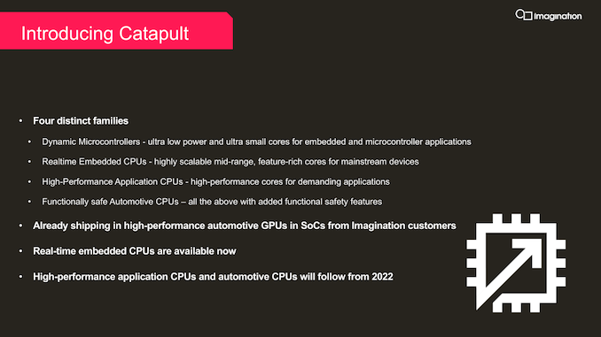
The current in-order core design supports up to 8 cores in a single cluster. The company didn’t quote any performance figures, though bear in mind this is a simple processor meant for microcontrollers and other very low power devices. Meanwhile, the core is available with ECC across both its L1 and TCM caches, as well as support for some of RISC-V’s brand-new extensions, such as the Vector computing extension, and potentially other extensions should customers ask for them.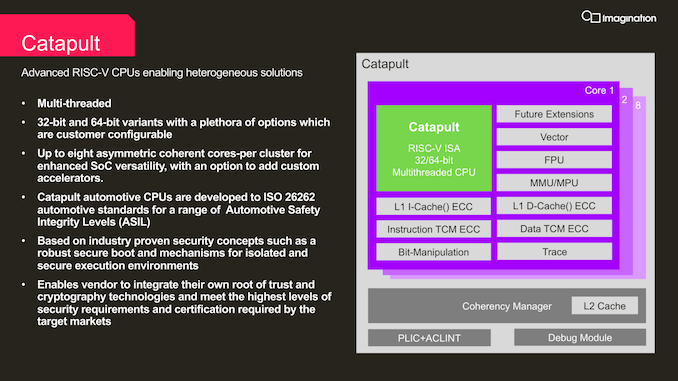
Following the current in-order core, Imagination has essentially three more core designs on their immediate roadmap. For 2022 the company is planning to release an enhanced version of the in-order core as an application processor-grade design, complete with support for “rich” OSes like Linux. And in 2023 that will be followed by another, even higher performing in-order core for the real-time and application processor markets. Finally, the company is also developing a much more complex out-of-order RISC-V core design as well, which is expected in the 2023-2024 timeframe. The out-of-order Catapult would essentially be their first take on delivering a high-performance RISC-V application processor, and like we currently see with high-performance cores the Arm space, has the potential to become the most visible member of the Catapult family.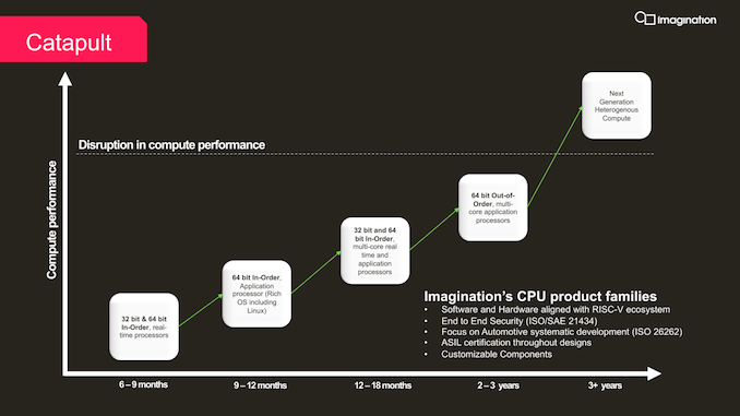
Farther out still are the company’s plans for “next generation heterogeneous compute” designs. These would be CPU designs that go beyond current heterogeneous offerings – namely, just placing CPU, GPU, and NPU blocks within a single SoC – by more deeply combining these technologies. At this point Imagination isn’t saying much more, but they are making it clear that they aren’t just going to stop with a fast CPU core.
Overall, these are all clean room designs for Imagination. While the company has long since sold off its Meta and MIPS CPU divisions, it still retains a lot of the engineering talent from those efforts – along with ownership of or access to a large number of patents from the area. So although they aren’t reusing anything directly from earlier designs, they are hoping to leverage their previous experience to build better IP sooner.
Of course, CPU cores are just one part of what it will take to succeed in the IP space; besides incumbent Arm, there are also multiple other players in the RISC-V space, such as SiFive, who are all vying for much of the same market. So Imagination needs to both differentiate themselves from the competition, and offer some kind of market edge to customers.
To that end, Imagination is going to be heavily promoting the possibilities for heterogenous computing designs with their IP. Compared to some of the other RISC-V CPU core vendors, Imagination already has well-established GPU and NPU IP, so customers looking to put together something more than just a straight CPU will be able to tap into Imagination’s larger library of IP. This does put the company more in direct competition with Arm (who already has all of these things as well), but then that very much seems to be Imagination’s goal here.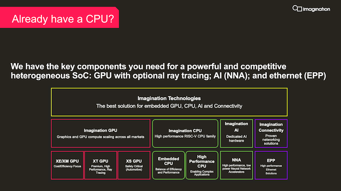
Otherwise, Imagination believes that their other big advantage in this space is the company’s history and location. As previously mentioned, Imagination holds access to a significant number of patents; so for clients who want to avoid extra patent licensing, they can take advantage of the fact that Imagination’s IP already comes indemnified against those patents. Meanwhile for chip designers who are based outside of the US and are weary of geopolitical issues affecting ongoing access to IP, Imagination is naturally positioned as an alternative there since they aren’t based in the US either – and thus access to their IP can’t be cut off by the US.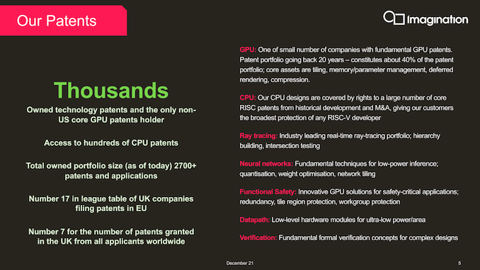
Wrapping things up, with the launch of their Catapult family of RISC-V CPU IP, imagination is laying out a fairly ambitious plan for the company for the next few years. By leveraging both their previous experience building CPUs as well as their current complementary IP like GPUs and NPUs, Imagination has their sights set on becoming a major player in the RISC-V IP space – and particularly when it comes to heterogeneous compute. Ultimately a lot will need to go right for the company before they can get there, but if they can succeed, then with their diverse collection of IP they would be in a rather unique position among RISC-V vendors.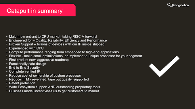
Gallery: Imagination Catapult Slide Deck


More...
-
12-14-21, 07:15 AM #11366
Anandtech: The Snapdragon 8 Gen 1 Performance Preview: Sizing Up Cortex-X2
At the recent Qualcomm Snapdragon Tech Summit, the company announced its new flagship smartphone processor, the Snapdragon 8 Gen 1. Replacing the Snapdragon 888, this new chip is set to be in a number of high performance flagship smartphones in 2022. The new chip is Qualcomm’s first to use Arm v9 as well as Samsung’s 4nm process node technology. In advance of devices coming in Q1, we attended a benchmarking session using Qualcomm’s reference design, and had a couple of hours to run tests focused on the new performance core, based on Arm’s X2 core IP.
More...
-
12-14-21, 10:29 AM #11367
Anandtech: Seagate Introduces AMD EPYC-Based Exos Application Platform: Up To 1.344PB
Seagate's Application Platform (AP) series of servers have targeted the market segments requiring tightly coupled storage and compute capabilities. The currently available SKUs - The Exos AP series with HDDs, and Nytro AP series with SSDs - are all based on Intel CPUs. That is changing today with the introduction of the Seagate Exos AP 5U84 based on the AMD EPYC Embedded 7292P processor.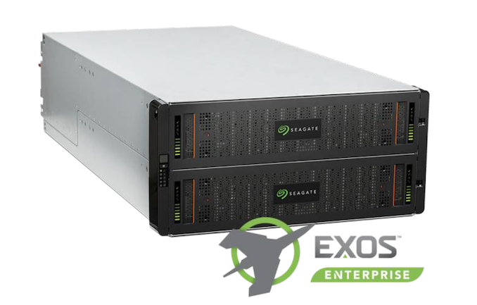
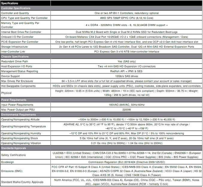
The Exos AP 5U84 equipped with the 2nd Gen. AMD EPYC platform enables a high-density building block for private clouds and on-premises equipment, with 84 3.5" HDD bays capable of storing up to 1.344PB (using Exos X16 HDDs) in a 5U form-factor. Capacity can further be expanded with EXOS E SAS expansion units. The platform includes redundancy options and all the other enterprise reliability functions expected in a storage / compute server. Networking with other rack components is enabled by dual port 25GbE controllers. The server processor can be configured for core counts of 8, 12, or 16 depending on required application compute requirements. The EPYC Embedded 7292P processor also include PCIe 4 lanes capable of delivering 200GbE network connectivity, if required.
Overall, the core count advantage and per-core power efficiency delivered by EPYC processors make it an ideal addition to Seagate's AP series. Given AMD's steady capturing of the server market, it doesn't come as a surprise to see the AMD EPYC Embedded 7292P getting adopted in the storage market.
More...
-
12-14-21, 10:11 PM #11368
Anandtech: SK Hynix to Manufacture 48 GiB and 96 GiB DDR5 Modules
Today SK Hynix is announcing the sampling of its next generation DDR5 memory. The headline is the commercialization of a new 24 gigabit die, offering 50% more capacity than the leading 16 gigabit dies currently used on high-capacity DDR5. Along with reportedly reducing power consumption by 25% by using SK Hynix’s latest 1a nm process node and EUV technology, what fascinates me most is that we’re going to get, for the first time in the PC space (to my knowledge), memory modules that are no longer powers of two.
For PC-based DDR memory, all the way back from DDR1 and prior, memory modules have been configured as a power of two in terms of storage. Whether that’s 16 MiB to 256 MiB to 2 GiB to 32 GiB, I’m fairly certain that all of the memory modules that I’ve ever handled have been powers of two. The new announcement from SK Hynix showcases that the new 24 gigabit dies will allow the company to build DDR5 modules in capacities of 48 GiB and 96 GiB.
To be clear, the DDR5 official specification actually allows for capacities that are not direct powers of two. If we look to other types of memory, powers of two have been thrown out the window for a while, such as in smartphones. However PCs and Servers, as least the traditional ones, have followed the power of two mantra. One of the changes in memory design that is now driving regular modules to non-power of two capacities is that it is getting harder and harder to scale DRAM capacities. The time it takes to figure out the complexity of the technology to get a 2x improvement every time is too long, and memory vendors will start taking those intermediate steps to get product to market.
In traditional fashion though, these chips and modules will be earmarked for server use first, for ECC and RDIMM designs. That’s the market that will absorb the early adopter cost of the hardware, and SK Hynix even says that the modules are expected to power high performance servers, particularly in machine learning as well as other HPC situations. One of the quotes on the SK Hynix press release was from Intel’s Data Center Group, so if there is any synergy related to support and deployment, that’s probably the place to start. A server CPU with 8x 64-bit channels and 2 DIMMs per channel gives 16 modules, and 16 x 48 GiB enables 768 GiB capacity.
As to when this technology will come to the consumer market, we’re going to have to be mindful of cost and assume that these chips will be used on high-cost hardware. So perhaps 48 GiB UDIMMs will be the first to market, although there’s a small possibility 24 GiB UDIMMs might make an appearance. Suddenly that 128 GiB limit on a modern gaming desktop will grow to 192 GiB.
Source: SKHynix Newsroom
More...
-
-
12-15-21, 02:42 PM #11370
Anandtech: Startup Showcases 7 bits-per-cell Flash Storage with 10 Year Retention
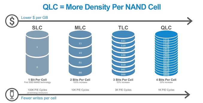
One of the key drivers to increase capacity in next generation storage has been to increase the number of bits that can be stored per cell. The easy jump of one to two bits-per-cell gives a straight 100% increase, in exchange for more control needed to read/write the bit but also limits the cell endurance. We’ve seen commercialization of storage up to four bits-per-cell, and talk about five. A Japanese company is now ready to start talking about their new 7 bits-per-cell solution.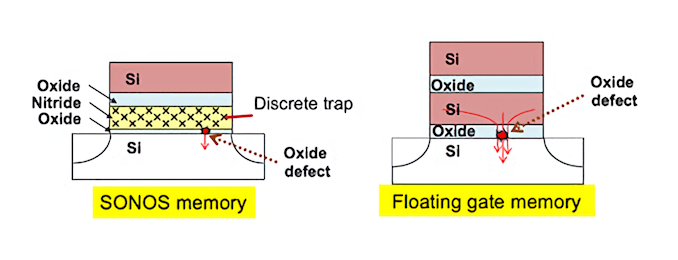
Moving from one to two bits-per-cell gives an easy doubling of capacity, and moving to three bits-per-cell is only another 50% increase. As more bits are added, the value of adding those bits diminishes, but the cost in the equipment to control the read and writes increases exponentially. There has to be a medium balance between how many bits-per-cell makes economic sense, and how much the control electronics costs to implement to enable those bits.
- 1 bit per cell requires detection of 2 voltage levels, base capacity
- 2 bit per cell requires detection of 4 voltage levels, +100% capacity
- 3 bit per cell requires detection of 8 voltage levels, + 50% capacity
- 4 bit per cell requires detection of 16 voltage levels, +33% capacity
- 5 bit per cell requires detection of 32 voltage levels, +25% capacity
- 6 bit per cell requires detection of 64 voltage levels, +20% capacity
- 7 bit per cell requires detection of 128 voltage levels, +16.7% capacity
Also, the more bits-per-cell, the lower the endurance – the voltage variation when you store many bits only has to drift slightly to get the wrong result, and so repeated read/writes to a high capacity cell will make that voltage drift until the cell is unusable. Right now the market seems happy with three bits-per-cell (3bpc) for performance and four bits-per-cell (4bpc) for capacity, with a few 2bpc designs for longer term endurance. Some of the major vendors have been working on 5bpc storage, although the low endurance may make the technology only good for WORM – write once, read many, which is a common acronym for the equivalent of something like an old-school CD or non-rewritable DVD.
Floadia Corp., a Series C startup from Japan, issued a press release this week to state that it has developed storage technology capable of seven bits-per-cell (7bpc). Still in the prototype stage, this 7bpc flash chip, likely in a WORM scenario, has an effective 10-year retention time for the data at 150C. The company says that a standard modern memory cell with this level of control would only be able to retail the data for around 100 seconds, and so the secret in the design is to do with a new type of flash cell they have developed.
The SONOS cell uses a distributed charge trap design relying on a Silicon-Oxide-Nitride-Oxide-Silicon layout, and the company points to an effective silicon nitride film in the middle where the charges are trapped to allow for high retention. In simple voltage program and erase cycles, the company showcases 100k+ cycles with a very low voltage drift. The oxide-nitride-oxide layers rely on SiO2 and Si3N4, the latter of which is claimed to be easy to manufacture. This allows a non-volatile SONOS cell to be used in NV-SRAM or embedded designs, such as microcontrollers.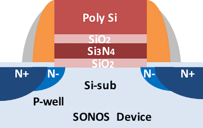
It’s actually that last point which means we’re a long time from seeing this in modern NAND flash. Floadia is currently partnering with companies like Toshiba to implement the SONOS cell in a variety of microcontrollers, rather than large NAND flash deployments, at the 40nm process node as embedded flash IP with compute-in-memory properties. Those aren’t at 7 bits-per-cell yet, to the effect that the company is promoting that two cells can store up to 8-bits of network weights for machine learning inference – when we get to 8 bits-per-cell, then it might be more applicable. The 10-year retention of the cell data is where it gets interesting, as embedded platforms will use algorithms with fixed weights over the lifetime of the product, except for the rare update perhaps. Even with increased longevity, Floadia doesn’t go into detail regarding cyclability at 7bpc at this time.
An increase from modern 3bpc to 6bpc NAND flash would afford a double density increase, however larger cells would be needed, which would negate the benefits. There’s also the performance aspect if the development of >4bpc ever made it to consumers, which hasn’t been touched upon.
It will be an interesting technology to follow.
Source: Floadia Press Release
More...


 Quote
Quote
Thread Information
Users Browsing this Thread
There are currently 15 users browsing this thread. (0 members and 15 guests)


Bookmarks