

Results 11,371 to 11,380 of 12094
Thread: Anandtech News
-
12-17-21, 01:32 PM #11371
Anandtech: NVIDIA Announces GeForce RTX 2050, MX570, and MX550 For Laptops: 2022's En
NVIDIA this morning had made an unexpected news drop with the announcement of a trio of new GeForce laptop GPUs. Joining the GeForce family next year will be a new RTX 2000 series configuration, the GeForce RTX 2050, as well as an update to the MX lineup with the addition of the GeForce MX550 and GeForce MX570. The combination of parts effectively provide a refresh to the low-end/entry-level segment of NVIDIA’s laptop product stack, overhauling these products in time for new laptops to be released next year.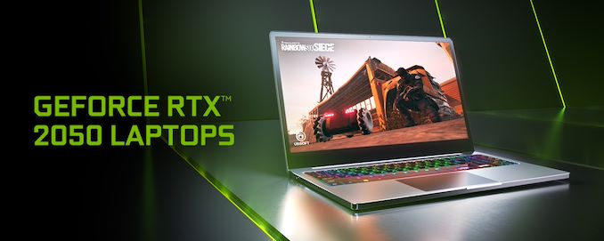
More...
-
12-17-21, 07:51 PM #11372
Anandtech: TSMC Unveils N4X Node: Extreme High-Performance at High Voltages
TSMC this week announced a new fabrication process that is tailored specifically for high-performance computing (HPC) products. N4X promises to combine transistor density and design rules of TSMC's N5-family nodes with the ability to drive chips at extra high voltages for higher frequencies, which will be particularly useful for server CPUs and SoCs. Interestingly, TSMC's N4X can potentially enable higher frequencies than even the company's next-generation N3 process.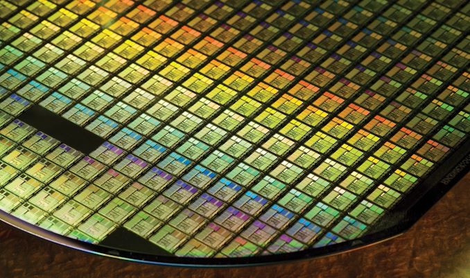
One of the problems that is caused by shrinking sizes of transistors is shrinking sizes of their contacts, which means increased contact resistance and consequent problems with power delivery. Various manufacturers use different ways of tackling the contact resistance issue: Intel uses cobalt contacts instead of tungsten contacts, whereas other makers opted to forming contacts using selective tungsten deposition technology. While these methods work perfectly for pretty much all kinds of chips, there are still ways to further improve power delivery for high-performance computing (HPC) designs, which are relatively immodest about the total about of power/voltage being used. This is exactly what TSMC did to its N4X node. But before we proceed to details about the new fabrication process, let us see what advantages TSMC promises with it.
TSMC claims that its N4X node can enable up to 15% higher clocks compared to a similar circuit made using N5 as well as an up to 4% higher frequency compared to an IC produced using its N4P node while running at 1.2V. Furthermore – and seemingly more important – N4X can achieve drive voltages beyond 1.2V to get even higher clocks. To put the numbers into context: Apple's M1 family SoCs made at N5 run at 3.20 GHz, but if these SoCs were produced using N4X, then using TSMC's math they could theoretically be pushed to around 3.70 GHz or at an even higher frequency at voltages beyond 1.2V.
TSMC does not compare transistor density of N4X to other members of its N5 family, but normally processors and SoCs for HPC applications are not designed using high-density libraries. As for power, drive voltages of over 1.2V will naturally increase power consumption compared to chips produced using other N5-class nodes, but since the node is designed for HPC/datacenter applications, its focus is to provide the highest performance possible with power being a secondary concern. In fact, total power consumption has been increasing on HPC-class GPUs and similar parts for the last couple of generations now, and there is no sign this will stop in the next couple of generations of products, thanks in part to N4X.
"HPC is now TSMC's fastest-growing business segment and we are proud to introduce N4X, the first in the ‘X’ lineage of our extreme performance semiconductor technologies," said Dr. Kevin Zhang, senior vice president of Business Development at TSMC. "The demands of the HPC segment are unrelenting, and TSMC has not only tailored our ‘X’ semiconductor technologies to unleash ultimate performance but has also combined it with our 3DFabric advanced packaging technologies to offer the best HPC platform."
In a bid to increase performance and make drive voltages of over 1.2V possible, TSMC had to evolve the entire process stack.Advertised PPA Improvements of New Process Technologies
Data announced during conference calls, events, press briefings and press releasesTSMC N5
vs
N7N5P
vs
N5N5HPC
vs
N5N4
vs
N5N4P
vs
N5N4P
vs
N4N4X
vs
N5N4X
vs
N4PN3
vs
N5Power -30% -10% ? lower -22% - ? ? -25-30% Performance +15% +5% +7% higher +11% +6% +15%
or
more+4%
or more+10-15% Logic Area
Reduction %
(Density)0.55x
-45%
(1.8x)
-
-0.94x
-6%
1.06x0.94x
-6%
1.06x
-
?
?0.58x
-42%
(1.7x)Volume
ManufacturingQ2 2020 2021 Q2 2022 2022 2023 H2 2022 H1
2024?H1 2024? H2 2022
- First, it redesigned its FinFET transistors and optimized them both for high clocks and high drive currents, which probably means reducing resistance and parasitic capacitance and boosting the current flow through the channel. We do not know whether it had to increase gate-to-gate pitch spacing and at this point TSMC does not say what exactly it did and how it affected transistor density.
- Secondly, it introduced new high-density metal-insulator-metal (MiM) capacitors for stable power delivery under extreme loads.
- Thirdly, it redesigned back-end-of-line metal stack to deliver more power to transistors. Again, we do not know how this affected transistor density and ultimately die sizes.
To a large degree, Intel introduced similar enhancements to its 10nm Enhanced SuperFin (now called Intel 7) process technology, which is not surprising as these are natural methods of increasing frequency potential.
What is spectacular is how significantly TSMC managed to increase clock speed potential of its N5 technology over time. A 15% increase puts N4X close to its next-generation N3 fabrication technology. Meanwhile, with drive voltages beyond 1.2V, this node will actually enable higher clocks than N3, making it particularly good for datacenter CPUs.
TSMC says that expects the first N4X designs to enter risk production by the first half of 2023, which is a very vague description of timing, as it may mean very late 2022 or early 2023. In any case, it usually takes a year for a chip to proceed from risk production to high-volume production iteration, so it is reasonable to expect the first N4X designs to hit the market in early 2024. This is perhaps a weakness of N4X as by the time its N3 will be fully ramped and while N4X promises to have an edge in terms of clocks, N3 will have a major advantage in terms of transistor density.
Source: TSMC
More...
-
12-22-21, 08:12 PM #11373
Anandtech: Qualcomms 8cx Gen 3 for Notebooks, Nuvia Core in 2022/2023
There are many column inches detailing Qualcomm’s design wins and marketing strategy, however to paint it all with a broad brush, it has often boiled down to ‘where can we stick our advanced wireless technology?’. The company has had great success with smartphones, cornering a large chunk of US market and sizeable numbers worldwide, and in the last few years has pivoted to new markets, such as automotive and virtual reality, but also tried to reinvigorate existing markets, such as notebooks and laptops. Since 2017, Qualcomm has wedged a new category into the market, dubbed the ‘Always Connected PC’, offering Windows control with extreme battery life and mobile connectivity. At this year’s Tech Summit, Qualcomm introduced its latest processor, however the real magic might come next year.
More...
-
12-23-21, 06:54 AM #11374
Anandtech: Samsung Announces First PCIe 5.0 Enterprise SSD: PM1743, Coming In 2022
Even though CES 2022 is technically still a couple of weeks away, CES-related announcements are already starting to roll in. Among these are Samsung, who is announcing their first PCIe 5.0 SSD for servers, the PM1743. Based around a new, unnamed PCIe controller, Samsung’s latest server SSD is pairing that with the company’s current (sixth) generation V-NAND. Based on their published specifications, Samsung is touting upwards of 70-90% better performance over their previous-generation drive based on the workload. And tying in with CES in a couple of weeks, the new drive has already been awarded a CES 2022 Innovation Award.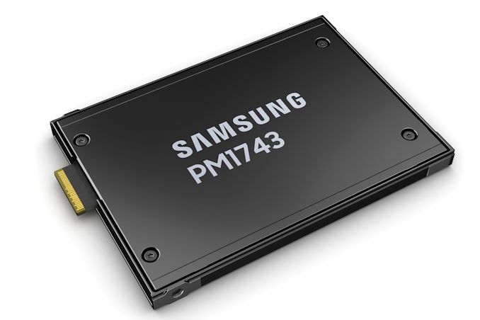
At a high level, the PM1743 is the successor to Samsung’s current PM1733 enterprise SSD. Whereas the existing drive is based around a PCIe 4.0 controller and Samsung’s 96L fifth-generation V-NAND, the PM1743 bumps this up to PCIe 5.0 and 128L sixth-generation V-NAND instead. Given the general nature of today’s announcement, the company isn’t offering detailed technical specifications on the drive’s architecture, but between the NAND and controller improvements, they would seem to largely be able to keep up with the additional bandwidth afforded by the move to PCIe 5.0.
On paper, the PCie 5.0 x4 link the drive uses can reach bandwidth rates as high as 15.76GB/sec. For the PM1743, in turn, Samsung is claiming peak sequential read rates of 13GB/second, and peak sequential write rates of 6.6GB/sec (presumably to the drive’s SLC cache). This adds up to 86% higher peak read speeds and 89% higher peak write speeds than the PM1733. Or to put that in terms of IOPS, Samsung is claiming that the new drive will be able to hit 2.5M IOPS on random reads, and 250K IOPS on random writes.
The updated Samsung controller is also embedding its own security processor and root of trust. Samsung’s announcement is light on the details, but at a high level, the company is doubling down on security by giving the drive a degree of security control independent of the host server.Samsung Enterprise SSD Specifications PM1743
(15.36TB)PM1733
(15.36TB)Form Factor U.2 or E3.S U.2 Interface PCIe 5.0 x4, NVMe PCIe 4.0 x4, NVMe Controller Unnamed Samsung PCIe 5.0 Samsung S4LR014 PCIe 4.0 NAND Flash Samsung 128L TLC? Samsing 96L TLC Sequential Read 13000 MB/s 7000 MB/s Sequential Write 6600 MB/s 3500 MB/s Random Read
IOPS2500k 1500k Random Write
IOPS250k 135k Power Active 30 W? 20 W Idle ? 8.5 W Write Endurance ? 28 PBW
1.0 DWPD for 5 Years
The company is also touting these updates as having improved the energy efficiency of the PM1743 by 30% over the PM1733, bringing it to 608MB/sec/watt. Given that data transfer rates have improved by upwards of 90% while power efficiency has only improved by 30%, it looks like the PM1743 will have a higher active power utilization rate than its predecessor. Doing some napkin math against the PM1733, which has a published figure of 20W, would put the active power of the PM1743 at around 30W.
Meanwhile, Samsung’s press release also confirms that the company has been working with Intel to validate the new drive. Samsung doesn’t go into any further details, but with Alder Lake (12th gen Core) already shipping now as the first mass market PCIe 5.0-capable platform, Samsung has presumably been testing against that, as well as the forthcoming Sapphire Rapids (next-gen Xeon) platform.
New for this generation of SSDs, Samsung will be offering the PM1743 in two form factors. The first will be the traditional 2.5-inch U.2 form factor. Meanwhile, joining U.2 will be E3.S, a newer 3-inch enterprise and data center form factor that is designed to be slightly larger than U.2 drives while incorporating a connector that can handle up to 16 lanes of PCIe. SSDs of course won’t use that many lanes, but it’s a form factor that both drive and system vendors have been pushing for, making it the front-runner as the eventual successor to U.2. Based on last year’s publication of the E3 2.0 specification, we had been expecting E3.S drives to land in early 2022, so Samsung is right on time.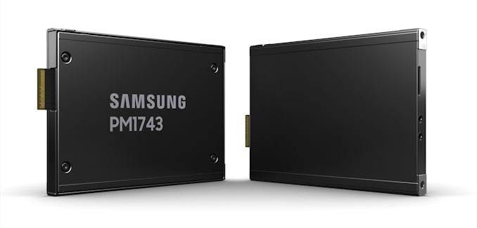
Finally, the PM1743 will be offered in capacities ranging from 1.92TB to 15.36TB, the same capacities the PM1733 is available at today. So although there is no capacity increase to speak of on a single drive level, since E3.S is half the thickness of a traditional 15mm U.2 drive, Samsung is touting the overall density improvements the new drive will afford. Essentially, if a server uses E3.S, it will be able to accommodate twice as many drives (and thus twice as much storage capacity) as a U.2 configuration.
The PM1743 is sampling now, and according to Samsung mass production will begin in the first quarter of next year.
More...
-
12-23-21, 11:56 AM #11375
Anandtech: Intel Alder Lake DDR5 Memory Scaling Analysis With G.Skill Trident Z5
One of the most agonizing elements of Intel's launch of its latest 12th generation Alder Lake desktop processors is its support of both DDR5 and DDR4 memory. Motherboards are either one or the other, while we wait for DDR5 to take hold in the market. While DDR4 memory isn't new to us, DDR5 memory is, and as a result, we've been reporting on the release of DDR5 since last year. Now that DDR5 is here, albeit difficult to obtain, we know from our Core i9-12900K review that DDR5 performs better at baseline settings when compared to DDR4. To investigate the scalability of DDR5 on Alder Lake, we have used a premium kit of DDR5 memory from G.Skill, the Trident Z5 DDR5-6000. We test the G.Skill Trident Z5 kit from DDR5-4800 to DDR5-6400 at CL36 and DDR5-4800 with as tight timings as we could to see if latency also plays a role in enhancing the performance.
More...
-
12-23-21, 06:08 PM #11376
Anandtech: AMD and GlobalFoundries Wafer Supply Agreement Updated Once More: Now $2.1
In a short note published by AMD this afternoon as part of an 8-K filing with the US Securities and Exchange Commission, AMD is disclosing that the company has once again updated its wafer supply agreement with long-time fab partner (and AMD fab spin-off) GlobalFoundries. Under the terms of the latest wafer supply agreement, AMD and GlobalFoundries are now committing to buying and supplying respectively $2.1 billion in wafers for the 2022 through 2025 period, adding an additional year and $500M in wafers to the previous agreement.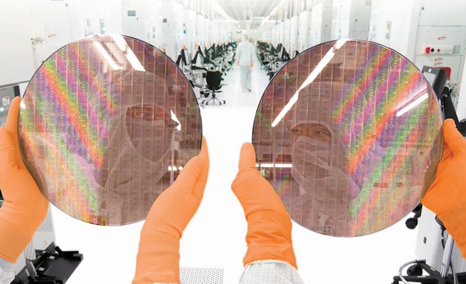
As a quick refresher, AMD and GlobalFoundries last inked a new wafer supply agreement (WSA) back in May of this year. That agreement further decoupled the two firms, ending any exclusivity agreements between the two and allowing AMD to use any fab for any node as they see fit. None the less, AMD opted to continue buying 12nm/14nm wafers from GlobalFoundries, with the two firms inking a $1.6 billion agreement to buy wafers for the 2022 through 2024 period.
Officially classified as the First Amendment to the Amended and Restated Seventh Amendment to the Wafer Supply Agreement, the latest amendment is essentially adding another year’s worth of production to the WSA. The updated amendment now goes through 2025, with AMD raising their 12nm/14nm wafer orders by $500 million to $2.1 billion. AMD and GlobalFoundries are not disclosing the specific per-year wafer supply targets, but the agreement essentially binds GlobalFoundries to supply AMD will a bit over $500M in wafers every year for the next 4 years.
Along with yearly spending commitments, the updated agreement also updates the price of said wafers, as well as the pre-payment requirements for 2022/2023. As with the specific number of wafers, AMD isn’t disclosing any further details here.
It’s also worth noting that, as with the previous agreement, these targets are binding in both directions. GlobalFoundries is required to allocate a minimum amount of its capacity to orders from AMD, and AMD in turn is required to pay for these wafers, whether they use this capacity or not. Given the ongoing chip crunch, it would seem that AMD is hedging their bets here, and locking in some additional supply a couple of years in advance. Though given the price re-negotiation, it would be interesting to see if AMD had to agree to higher overall prices in order to secure a larger supply of wafers from GlobalFoundries.AMD/GlobalFoundries Wafer Share Agreement History Amendment Date December 2021 May 2021 January 2019 Total Order Value $2.1B $1.6B N/A Start Date 2022 2022 2019 End Date 2025 2024 2024 GlobalFoundries Exclusivity? No No Partial
(12nm and larger)
Past that, AMD isn’t currently disclosing what they’ll be using the additional wafer capacity for – though they did clarify that it has nothing to do with acquisition target Xilinx. AMD currently uses GlobalFoundries’ 12nm/14nm processes for early-generation Ryzen products as well as the I/O dies for AMD’s current-generation Ryzen and EPYC CPUs. However under normal circumstances, we would expect demand for those products to be tapering off, especially by the 2024/2025 timeframe. The 12nm/14nm processes are already dated and are getting older still, so it’s unclear if this is AMD developing some backup plans to deal with the chip crunch, or if they are expecting demand for current 12/14 products to persist (e.g. if they need to produce their current long-term embedded products in larger numbers).
Baring any further amendments to the WSA, the current agreement between AMD and GlobalFoundries will now expire on December 31st, 2025.
On December 23, 2021, Advanced Micro Devices, Inc. (the “Company”) entered into the First Amendment (the “Amendment”) to its Amended and Restated Seventh Amendment to the Wafer Supply Agreement (the “A&R Seventh Amendment”) with GLOBALFOUNDRIES Inc. (“GF”) to extend GF’s capacity commitment and wafer pricing to the Company.
The Amendment modifies certain terms of the Wafer Supply Agreement applicable to wafer purchases at the 12 nm and 14 nm technology nodes by the Company for the period commencing on December 23, 2021 and continuing through December 31, 2025. GF agreed to increase the minimum annual capacity allocation to the Company for years 2022 through 2025. Further, the parties agreed to new pricing and annual wafer purchase targets for years 2022 through 2025, and modified the pre-payments agreed to by the Company to GF for those wafers in 2022 and 2023. The Amendment does not affect any of the prior exclusivity commitments that were removed under the A&R Seventh Amendment. The Company continues to have full flexibility to contract with any wafer foundry with respect to all products manufactured at any technology node. The Company currently estimates that it will purchase approximately $2.1 billion of wafers in total from GF for years 2022 through 2025 under the Amendment.
More...
-
12-29-21, 07:01 PM #11377
Anandtech: Intel Sells SSD Business to SK hynix as new Subsidiary Solidigm
In a brief news release from Intel this afternoon, the chip firm has announced that it has closed on the first stage of its deal to sell its SSD business to SK hynix. As of today, SK hynix has now formally acquired the bulk of Intel’s NAND and SSD businesses, as well as the company’s NAND fab in Dalian, China. Intel will continue to hold a small stake until 2025, and in the meantime Intel’s former SSD assets have been spun-off into a new SK hynix subsidiary, Solidigm.
The Intel-SK hynix deal was first announced in October of 2020, with the two companies inking a deal to transfer over Intel’s NAND and SSD operations over to SK hynix over a several year timeframe. The deal, valued at $9 billion, would see Intel retain all of their Optane/3D XPoint technology and patents, while SK Hynix would receive all of Intel’s NAND-related business, including the Dalian NAND fab and Intel’s SSD business interests.
Now, with approval of the deal from all of the necessary regulatory bodies, the two companies have been able to close on the first part of the deal. The “first closing,” as Intel puts it, has transferred the Dalian fab as well as part of Intel’s SSD IP portfolio to SK hynix. Some employees are also being transferred – essentially all those who aren't working for the fab or are involved in R&D. In return, SK hynix has paid Intel the first $7 billion of the deal.
The rest of the deal is set to close in three and a half years from now, in or around March of 2025. From now until then, Intel will continue to use the Dalian fab to manufacture NAND wafers. To do so, Intel has held on to some of their NAND-related IP, their R&D employees, and the fab employees. All of those assets will then finally be transferred to SK hynix once the deal fully closes and SK hynix pays Intel the final $2 billion.
Finally, SK hynix is taking the Intel assets they’ve acquired thus far and placing them into a new spin-off company, Solidigm. The standalone subsidiary, whose name is apparently a play on “paradigm” and “solid state storage” has setup shop in San Jose, and is being run by former Intel Non-Volatile Memory Solutions Group SVP and GM, Rob Crooke. Solidigm, in turn, has inherited Intel’s current NAND SSD product lineup; so Intel’s 660p and 670p client SSDs, as well as their D3/D5/D7 data center SSDs, are now in the process of becoming Solidigm products.
More...
-
12-30-21, 10:27 AM #11378
Anandtech: CPU Year In Review 2021: Efficient Cores Are The New Bling
As far as most years ago, 2021 has been an up and down year when it comes to the desktop CPU market. At the beginning of the year, the best CPUs on the market were almost impossible to find, and when they were in stock, it was only above the suggested pricing. Now at the end of the year, processors are plentiful, but the needle has swung in the other direction when it comes to performance. Here’s a rundown of the fun year that 2021 has been.
More...
-
12-30-21, 03:36 PM #11379
Anandtech: ASUS Demonstrates DDR5 to DDR4 Converter Card
One of the key issues with purchasing a modern Alder Lake system today is the cost of the memory, especially when an enthusiast wants to use DDR5. Due to component shortages, particularly the power management controllers that each DDR5 module needs, costs of DDR5 are quickly rising, with some scalpers looking for $1000+ for basic memory kits. The solution to this has been to recommend that users look to pair Alder Lake with DDR4 memory, which although it isn’t the latest, is the more cost effective scenario. The downside to this solution is that the user has a DDR4-only motherboard, and not the next generation DDR5. That might become a solved issue soon enough, however.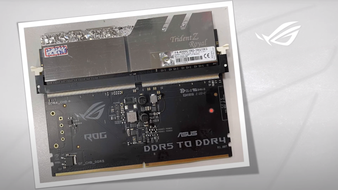
In a preview video on YouTube posted today by Bing, who I believe is an ASUS ROG employee, the company has been working on a solution to allow users that buy ASUS Z690 motherboards built on DDR5, to run DDR4 in them. Because Intel limited the platform to either DDR5 or DDR4 per motherboard, there’s no way to run both, until now. In the video, Bing describes the new add-in card they’ve been prototyping.
The use case is fairly simple – have a DDR5 board like the ROG Apex, put the carrier card in a memory slot, and place the qualified DDR4 in the top.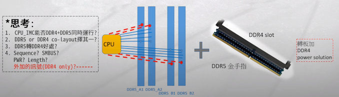
Obviously, the situation here is more complex than simply using this carrier card. DDR5 and DDR4 are more than simply a notch difference between them – DDR4 is a single 64-bit memory channel per module, while DDR5 is dual 32-bit channel per module. The key issue is that DDR5 does power management per module, where DDR4 relies on power management on the motherboard, so that has to be taken into consideration. Also, adding in a carrier card extends memory traces, which could degrade the quality of the signal.
What ASUS does here is use a special BIOS revision to allow the ROG Apex DDR5 to run in DDR4 mode. This means that the traces to the memory slots, although laid out for DDR5 operation, are switched into DDR4 mode. Then, on the carrier card, this takes the 5V power signal and runs it through the equivalent of motherboard power management, and controls the data lines to maintain integrity for signal, latency, power, etc.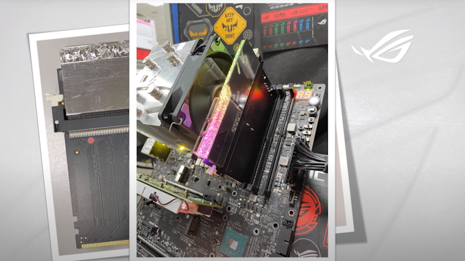
Bing explains in the video that this is still very much a prototype. It looks like they’re focusing to get it to work on one motherboard with one memory kit first, before optimizing it. Bing states that the carrier card is very tall, and there is room for optimization to make it smaller in the future before ASUS might offer it as a retail product. Also a wider range of validation is likely needed as well.
The video goes to show with a single DDR4 module in the carrier card the system running at DDR4-4400 with a Core i5-12600K. To confirm DDR5 still works, the system is shown running dual modules of DDR5-4400, at least to the BIOS screen. If these modules come to market, they are still in early prototypes, and ASUS will likely judge feasibility and demand for them for pricing.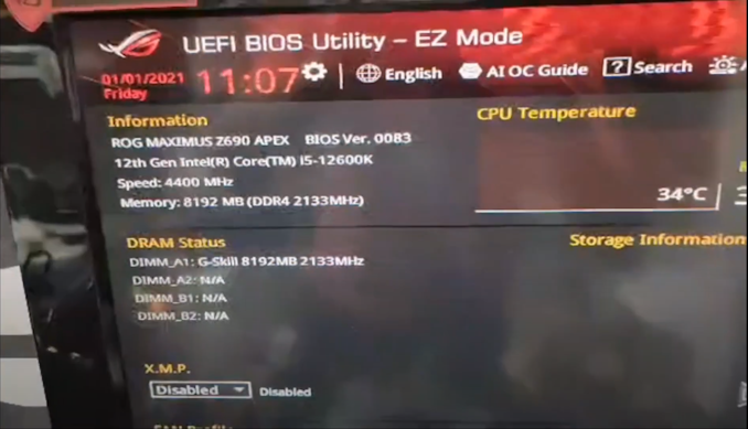
Source: YouTube (in Mandarin)
More...
-
12-30-21, 07:27 PM #11380
Anandtech: AMD-Xilinx Acquisition Now Expected to Close in Q1 of 2022
AMD this afternoon has sent out a brief update to the public and investors, offering an update on the status of the ongoing Xilinx acquisition. AMD’s purchase of the FPGA maker, which was previous expected to close by the end of this year, is now expected to close in the first quarter of 2022. Attributing the setback to delays in regulatory approval, AMD believes they’ll be able to finally secure the necessary approval for the $35 billion deal next quarter.
As a quick refresher, AMD first announced their intention to buy Xilinx back in October of 2020. The FPGA maker was a lucrative target for AMD, whose sales (and market capitalization) have been growing by leaps and bounds over the last few years. This has brought AMD to the point where they are looking at diversification, as well as covering any gaps in their product lineup that would be holding them back in the server market. As the plan goes, acquiring Xilinx, will allow AMD to offer FPGAs alongside (and potentially integrated with) their current CPU and GPU/accelerator products.
The deal was previously expected to close by the end of 2021, and AMD has remained very tight lipped on the matter outside of their initial announcement. None the less, acquiring the necessary regulatory approval is apparently taking AMD longer than planned. According to the company they are not expecting to need to change the deal or alter any of its terms, but they will need another quarter to get the last approvals required to close the deal.
“We continue making good progress on the required regulatory approvals to close our transaction. While we had previously expected that we would secure all approvals by the end of 2021, we have not yet completed the process and we now expect the transaction to close in the first quarter of 2022. Our conversations with regulators continue to progress productively, and we expect to secure all required approvals.”
There are no additional changes to the previously announced terms or plans regarding the transaction and the companies continue to look forward to the proposed combination creating the industry’s high-performance and adaptive computing leader.
More...


 Quote
QuoteThread Information
Users Browsing this Thread
There are currently 21 users browsing this thread. (0 members and 21 guests)


Bookmarks