

Results 11,411 to 11,420 of 12094
Thread: Anandtech News
-
01-18-22, 06:28 AM #11411
Anandtech: ASRock Unveils DeskMeet SFF PC Platform with Intel B660 / AMD X300 Chipset
ASRock has been at the forefront of the small form-factor (SFF) PC revolution right from the Sandy Bridge days. Starting with the Core HT series in the early 2010s, the company moved on to the Beebox (NUC clones) , and recently settled on the DeskMini lineup (based on mini-STX boards). At the 2022 CES, the company is introducing a new SFF PC - the DeskMeet. It is meant to be a step up from the DeskMini - allowing for a custom motherboard, more RAM slots, and space for discrete GPUs.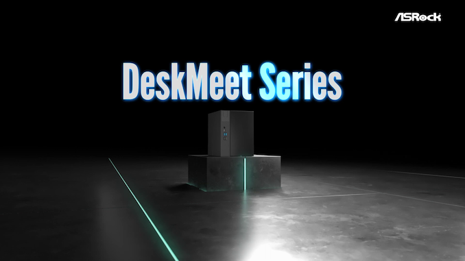
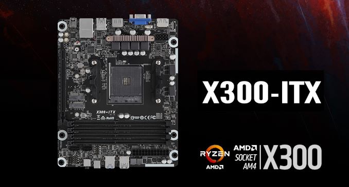
ASRock is delivering all this in a chassis with a 8L volume with two configurations - one based on the Intel B660 platform, and another based on the AMD X300 chipset (AM4 socket). The key specifications of the two systems are summarized in the table below.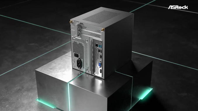
While the absence of high-end I/O ports like Thunderbolt 4 and USB 3.2 Gen 2x2 or high-end wired networking is a tad disappointing, ASRock is making up for that by supporting PCIe expansion cards and quad-DIMM configurations for up to 128GB of RAM. ASRock calls these boards -ITX, but they are not truly mini-ITX in size.ASRock DeskMeet SFF PCs - 2022 Lineup DeskMeet B660 DeskMeet X300 CPU Intel 12th Gen Core Processors AMD AM4 Socket Ryzen Desktop APUs / CPUs (Ryzen 2000/3000/4000/5000) (up to 65W) Cooler Stock coolers / up to 54mm in height Chipset Intel B660 AMD X300 Memory Dual-Channel DDR4
4x DDR4 DIMM Slots (up to 128GB)
non-ECC, un-bufferedDual-Channel DDR4
4x DDR4 DIMM Slots (up to 128GB)
ECC / non-ECC, un-bufferedDiscrete GPU Support Up to 200mm in length Networking 1x RJ-45 Gigabit LAN (Intel I219V)
M.2 2230 Slot for Wi-Fi + BT Module1x RJ-45 Gigabit LAN (Realtek RTL8111H)
M.2 2230 Slot for Wi-Fi + BT ModuleStorage 3x SATA III 6Gbps
1x Hyper M.2 2280 (PCIe Gen 4 x4 / SATA III 6Gbps)
1x Hyper M.2 2280 (PCIe Gen 4 x4)2x SATA III 6Gbps
1x Ultra M.2 2280 (PCIe Gen 3 x4)Expansion Slots 1x PCIe 4.0 x16 1x PCIe 3.0 x16 Audio Codec Realtek ALC897 Front I/O 1x Headset
1x USB 3.2 Gen 1 Type-C
2x USB 3.2 Gen 1 Type-A
2x USB 2.0 Type-ARear I/O 1x DP 1.4a
1x HDMI 2.0a
1x D-Sub
2x USB 2.0 Type-A
2x USB 3.2 Gen 1 Type-A
1x RJ-45<
HD Audio Jack (Line In / Speaker / Microphone)/td>1x DP 1.4a
1x HDMI 2.0a
1x D-Sub
2x USB 2.0 Type-A
2x USB 3.2 Gen 1 Type-A
1x RJ-45<
HD Audio Jack (Line Out)/td>Power Supply 500W (80+ Bronze / 550W Peak) Dimensions 168mm x 219.3mm x 218.3mm
The space inside the chassis allows for multiple configurations - with or without a discrete GPU, ability to mount multiple 3.5" drives etc. The DeskMeet aims to provide as many features and flexibilities as possible within the constraints dictated by the chipsets.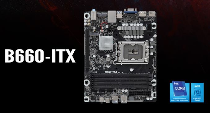
In other ASRock SFF PC news, the company has also released a new mini-STX platform using the Intel B660 chipset for Alder Lake. The DeskMini B660 retains the chassis design of the previous generations.
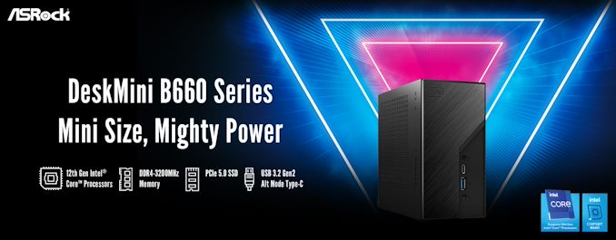
Thanks to the use of the B660 chipset, the front Type-C port is now USB 3.2 Gen 2x2 (20 Gbps). The rear Type-C port supports 10 Gbps data transfer alone with DP 1.4a, and 60W PD. The other interesting aspect is the availability of a PCIe 5.0 M.2 2280 SSD slot, in addition to a PCIe 4.0 M.2 2280 one. A M.2 2230 slot for Wi-Fi, and a gigabit Ethernet slot are the regular features retained from the previous DeskMini units.
After a couple of years of staid SFF PCs with rather unimpressive updates, ASRock is promising interesting offerings in 2022. No specific launch prices or retail availability timelines were provided for the new systems.
Gallery: ASRock Unveils DeskMeet SFF PC Platform with Intel B660 / AMD X300 Chipsets


More...
-
01-18-22, 12:40 PM #11412
Anandtech: The MSI MEG Z690 Unify (DDR5) Motherboard Review: The All-Black Option
With the Unify, we are looking at a premium model with support for DDR5 memory, but it doesn't feature any RGB LED lighting. The MSI MEG Z690 Unify represents MSI's Enthusiast Gaming series, which combines elements of an enthusiast-level motherboard, but with all the features designed for users to make the most of the latest controller sets and 12th gen features. Some of the features include five M.2 slots, support for DDR5-6666 memory, dual 2.5 GbE and Wi-Fi 6E networking, as well as an advertised 21-phase power delivery.
More...
-
01-19-22, 10:05 AM #11413
Anandtech: Launching Today: AMD's Radeon RX 6500 XT, Starring Navi 24
Following its announcement back at CES, today AMD is formally launching the entry-level member of its Radeon RX 6000 series of video cards: the Radeon RX 6500 XT. Based on AMD’s new Navi 24 GPU – the first GPU made on TSMC’s N6 process – AMD is broadening their desktop video card lineup by adding a new low-end option. And while the $199 price tag is unlikely to arouse much enthusiasm, the addition of another video card SKU – and one that’s relatively useless for crypto mining – is likely to be a welcome relief for the capacity-constrained discrete video card market.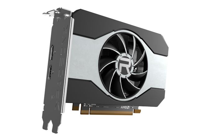
More...
-
01-19-22, 10:05 AM #11414
Anandtech: Intel Expands 12th Gen Core to Ultraportable Laptops, from 5-cores at 9 W
Over the years Intel has prided itself on its ability to provide processors that fit into the ultraportable, professional market. We’re talking thin and light designs with obscene levels of performance and battery life for the form factor. It’s so important to Intel, that over the years they’ve produced several design and validation standards relating to how the best ultraportables should be developed, such as low power displays, the best connectivity standards, and approaching all-day battery life. It surprised me somewhat that Intel didn’t really discuss its next generation of processors for these devices at CES at the beginning of the year, focusing their keynote almost entirely on the 45 W prosumer and workhorse designs instead. To find out about the more mainstream and ultraportable silicon, we had to dig into the back end of our press deck to get details.
More...
-
01-20-22, 12:19 PM #11415
Anandtech: Intels Next Gen Bitcoin ASIC called BZM2: Built on 7nm, 137 GigaHash/sec
It has been noted in the media that at the upcoming ISSCC conference at the end of February, Intel is set to give a talk entitled ‘Bonanza Mine: An Ultra-Low Voltage Energy Efficient Bitcoin Mining ASIC’. It already has a lot of attention, as it confirms the fact that Intel is working towards blockchain-enabling hardware. Through a number of channels, we’ve been able to acquire more details about this chip ahead of the conference.
More...
-
01-21-22, 01:05 PM #11416
Anandtech: Intel Announces Ohio Fab Complex: 2 New Fabs For $20B, And Space For More
With fab expansions on tap across the entire semiconductor industry, Intel today is laying out their own plans for significantly increasing their production capacity by announcing their intention to build a new $20 billion fab complex in Ohio. With the paperwork already inked and construction set to begin in late 2022, Intel will be building two new leading-edge fabs in their new Ohio location to support future chip needs. And should further demand call for it, the Ohio complex has space to house several more fabs.
Intel’s announcement follows ongoing concerns about chip fab capacity and national security, as like other chip fabs, Intel is looking to expand their capacity in future years amidst the current chip crunch. All the while, the United States government has become increasingly mindful about how much chip production takes place in geopolitically tricky Taiwan, placing additional pressure on firms to build additional fabs within the US. To that end, Intel has been not-so-secretly undertaking a search to find a good location for a new fab campus, and they have finally found their answer in Ohio.
The new site, Intel’s first new manufacturing site location in 40 years, is located in New Albany, Ohio, just outside of Columbus. Up until now, all of Intel’s major chip fab sites have been in the western United States – Oregon, Arizona, and at one point, Silicon Valley – so the Ohio site is a significant move for the company. All told, the Ohio “mega-site”, as Intel likes to call it, covers nearly 1000 acres. And while Intel is only initially planning for two fabs, the site offers plenty of room to grow, offering enough space for a total of 8 fabs.
The immediate goal of the company – and the crux of today’s announcement – revolves around the building of two new leading-edge fabs at the Ohio location. According to Intel, these two fabs will begin construction late this year, with production coming online in 2025. The company isn’t formally stating what the initial process node will be – instead saying that it will be using the "industry's most advanced transistor technologies" – however if the company is indeed building truly bleeding-edge fabs, then 2025 lines up with Intel’s 18A process, which will be 4 generations newer than what Intel is using now (Intel 7).
Altogether, Intel expects the project to cost about $20 billion, which is similar to what Intel will be spending for its two new Arizona fabs, which were announced just under a year ago. And further down the line, should Intel opt to fill the rest of the property with the other 6 fabs that the site can support, the company expects that the total price tag could reach nearly $100 billion. Ultimately, the company is making it clear that they are priming the site not just to met their mid-term production needs with the initial two fabs, but are making sure to have the space ready for further capacity expansion over the long-term.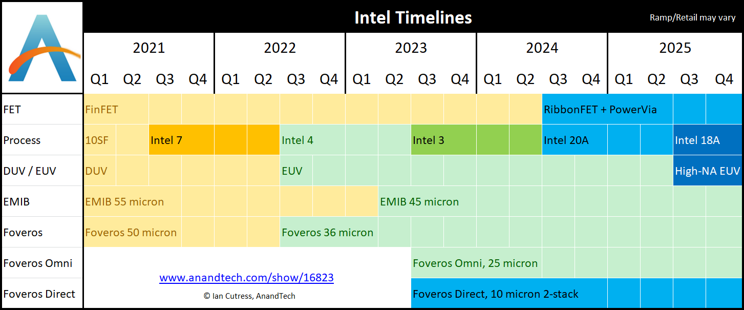
As to whether Intel eventually builds those further 6 fabs, that will depend on a few factors. Key among these will be demand from Intel Foundry Services clients; while Intel will be using some of the Ohio site’s capacity for their own needs, the site will also be used to fab chips for IFS customers. If Intel’s bid to break into the contract fab business is successful, and the company is able to woo over additional clients/orders, then they will need to build additional fabs to meet that demand.
Also hanging in the balance is what the US Government opts for, both in terms of orders and incentives. The Ohio fabs will be used for domestic production of sensitive chips, as the US looks to secure its supply lines. Meanwhile the CHIPS for America Act and its 53 billion in incentives will also be a. Intel for its part isn’t playing coy about its interest in the CHIPS money, explicitly stating that “The scope and pace of Intel’s expansion in Ohio, however, will depend heavily on funding from the CHIPS Act”. In some respects Intel is taking a bit of a gamble by investing in the Ohio location before any CHIPS funding is approved – on a pure cost basis, overseas production is traditionally cheaper – so there is certainly a political element in announcing these fabs and selecting an Ohio location. And as an added incentive to the US Government, Pat Gelsinger has told Time that Intel would even be interested in bringing some chip packaging, assembly, and testing back to the US if the CHIPS Act were funded, which in turn would allow Intel to do every last step of production within the US.
But more immediately, Intel’s focus is on getting its first two Ohio fabs up and running. Along with building the facilities they’ll need a workforce to operate them, and as a result the company is also pledging $100M over a decade in funding for local educational efforts. As with similar local industry efforts, that investment would be focused on helping local colleges and universities establish semiconductor manufacturing curricula to help train the technical workforce required.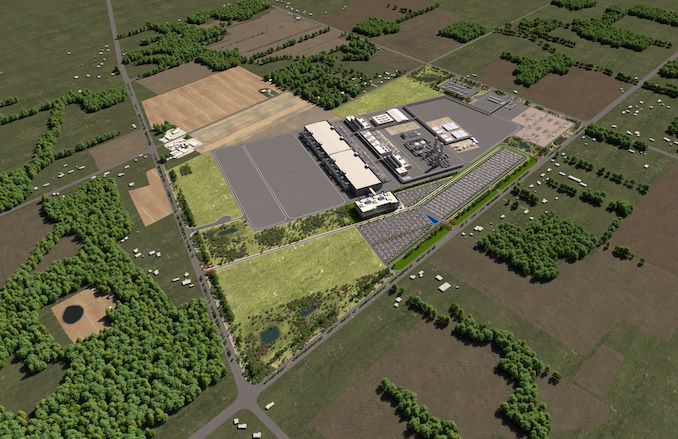
And while outside of Intel’s own investment scope, the creation of their Ohio fab complex means that Intel’s suppliers are also coming along for the ride. According to the company, Air Products, Applied Materials, LAM Research and Ultra Clean Technology have all indicated that they’ll be setting up facilities in the area. All of which the company is using to further underscore the size of the project and the value it brings to the area – and why they deserve that CHIPS Act funding.
Ultimately, the addition of a third US fab site and two more fabs to Intel’s portfolio is the latest step Intel has taken under Pat Gelsinger’s IDM 2.0 strategy. Gelsinger opted to go all-in on having Intel fab chips for themselves and others, and this is the kind of expansion that Gelsinger has been alluding to as necessary to make IDM 2.0 a reality. Taken altogether, Intel now has 4 leading-edge fabs set to come online in the 2024-2025 timeframe, and with any luck on Intel’s part, there will be room for several more to come.
Source: Intel
More...
-
01-24-22, 12:43 PM #11417
Anandtech: Interview with Intels Dan Ragland, Head of Overclocking: Tuning Alder Lak
The topic of overclocking has been an interesting one to track over the years. Over a decade ago, when dealing with 2-4 core processors, an effective overclock gave a substantial performance uplift, often allowing a $200 processor to perform like the one that cost $999. However, core counts have increased over the last couple of years, but also companies like Intel are getting better at understanding their silicon, and are able to ship it out of the box almost at the silicon limit anyway. So what use is overclocking? We turned to Dan Ragland, who runs Intel’s Overclocking Lab in Hillsboro, Oregon, to find out what overclocking now means for Intel, what it means for Alder Lake, but also how Intel is going to approach overclocking in the future.
More...
-
01-25-22, 08:54 AM #11418
Anandtech: Intel Alder Lake-H Core i9-12900HK Review: MSI's Raider GE76 Goes Hybrid
At CES this year, Intel officially announced its expanded Alder Lake lineup including the performance-laptop focused H-Series processors, which traditionally fit in the 45-Watt range. Today we finally get to take a look at the 12th generation H-Series processors, the first mobile incarnation of Alder Lake, and see how Intel's fastest mobile platform stacks up to not only Intel’s previous 11th generation Tiger Lake platform, but also AMD’s Ryzen 5000 series.
More...
-
01-25-22, 12:36 PM #11419
Anandtech: G.Skill Blitzes DDR5 World Record With Trident Z5 at DDR5-8888
For users buying a memory kit of DDR5, if they want to adhere to Intel specifications, will buy a DDR5-4800 kit. Though through XMP, there are other faster kits available - we've even tested G.Skill's DDR5-6000 kit in our memory scaling article. But going above and beyond that, there's overclocking.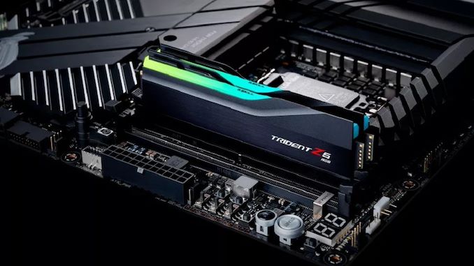
Back in November 2021, extreme overclocker 'Hocayu' managed to achieve DDR5-8704 using G.Skill's Trident Z5 DDR5-6000 memory. As always with these records, they are made to be broken, and fellow Hong-Kong native lupin_no_musume has managed to surpass this with an impressive DDR5-8888, also using G.Skill Trident Z5 memory, with an ASUS's ROG Maximus Z690 Apex motherboard, Intel's Core i9-12900K processor, and some liquid nitrogen.
Without trying to sound controversial, indeed, extreme overclocking isn't as popular as it once was. That isn't to say it doesn't have a purpose - using sub-ambient cooling methods such as liquid nitrogen, dry ice, and even liquid helium can boost frequencies on processors and graphics cards well beyond what's achievable with standard cooling. Doing this not only shows the potential of hardware, but it also gives companies 'bragging rights' as being the proud owners of overclocking world records. Car companies boast about the best Nürburgring record for a variety of categories, or tuning their mainstream offerings, in a similar fashion.
This not only pushes the boundaries of what DDR5 memory is capable of, but it's also an impressive feat given DDR5 is relatively nascent. For reference, going from DDR5-6000 to DDR5-8888 represents an overclock of around 48% over the XMP profile and a crazy 85% overclock over the JEDEC specification of DDR5-4800. It should be worth noting that this is an all out data rate record regardless of latency, which in this case was increased to 88 over the standard 40, for stability. Going back to the car analogy, this would be akin to speed records on the drag strip, rather than on the oval.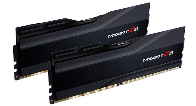
G.Skill Trident Z5 DDR5-6000 (2 x 16 GB) memory kit.
While speeds of DDR5-8888 are not attainable in the form of purchasable memory kits for Alder Lake, G.Skill did unveil a retail kit that tops out at DDR5-7000. We also reported back in November 2021 that S.K. Hynix was planning for DDR5-8400 at 1.1 volts, but that's actually part of the entended JEDEC specifications for when processors get verfied at that speed.
Source: G.Skill
Related Reading- Intel Alder Lake DDR5 Memory Scaling Analysis with G.Skill Trident Z5
- ASUS Demonstrates DDR5 to DDR4 Converter Card
- G.Skill Unveils Premium Trident Z5 and Z5 RGB DDR5 Memory, Up to DDR5-6400
- Insights into DDR5 Sub-timings and Latencies
More...
-
01-25-22, 12:36 PM #11420
Anandtech: Vulkan 1.3 Specification Released: Fighting Fragmentation with Profiles
Khronos this morning is taking the wraps off of Vulkan 1.3, the newest iteration of the group’s open and cross-platform API for graphics programming.
Vulkan 1.3 follows Khronos’s usual 2 year release cadence for the API, and it comes at a critical juncture for the API and its future development. Vulkan has been a full and official specification since 2016, turning 6 years old this year. This has given the API plenty of time to mature and have its kinks worked out, as well as to be adopted by software and hardware developers alike. But it also means that with the core aspects of the API having been hammered out, where to go next has become less obvious/harmonious. And with the API in use for everything from smartphones to high-end PCs, Vulkan is beginning to fragment at points thanks to the wide range of capabilities in devices.
As a result, for Vulkan 1.3, Khronos and its consortium members are taking aim at the future of the API, particularly from a development standpoint. Vulkan is still in a healthy place now, but in order to keep it that way, Khronos needs to ensure that Vulkan has room to grow with new features and functionality, but all without leaving behind a bunch of perfectly good hardware in the process. Thankfully, this isn’t a new problem for the consortium – it’s something virtually every standard faces if it lives long enough to become widely used – so Khronos is hitting the ground running with some further refinements to Vulkan.
Vulkan 1.3 Core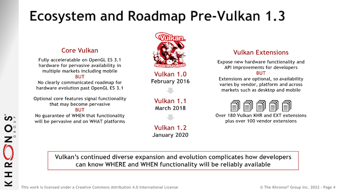
But before we get into Khronos’s fragmentation-fighting efforts, let’s first talk about what’s coming to the Vulkan 1.3 core specification. The core spec covers all of the features a Vulkan implementation is required to support, from the most basic smartphone to the most powerful workstation. As a result it has a somewhat narrow scope in terms of graphical features, but as the name says on the tin, it’s the common core of the API.
As with previous versions of the spec, Khronos is targeting this to work on existing Vulkan-compliant hardware. Specifically, Vulkan 1.3 is designed to work on OpenGL ES 3.1 hardware, meaning that of the new features being rolled into the core spec, none of them can be beyond what ES 3.1 hardware can do.
Consequently, Vulkan 1.3’s core spec isn’t focused on adding new graphical features or the like. By design, graphical feature additions are handled by extensions. Instead, the 1.3 core spec additions are largely a quality-of-life update for Vulkan developers, with a focus on adding features that simplify some aspect of the rendering process or add more control over it.
Altogether, Khronos is moving 23 existing extensions into the Vulkan 1.3 core spec. Most of these extensions are very much inside-baseball fodder for graphics programmers, but there are a couple of highlights. These include the integer dot product function, which is already widely used for machine learning inference on GPUs, as well as support for dynamic rendering. These functions already exist as extensions – so many developers can and are already using them – but by moving them into the core spec, they are now required for all Vulkan 1.3 implementations, opening them up to a wider array of developers.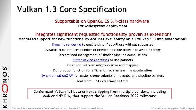
But arguably the single most important addition coming to Vulkan isn’t an extension being promoted into the core specification. Rather, it’s entirely new functionality entirely, in the form of feature profiles.
Vulkan Profiles: Simplifying Feature Sets and Roadmaps
Up until now, Vulkan has not offered a concept of feature levels or other organizational grouping for additional feature sets. Beyond the core specification, everything in Vulkan is optional, all 280+ extensions. Meaning that for developers who are building applications that tap into features that go beyond the core spec – which has quickly become almost everything not written for a smartphone – there hasn’t been good guidance available on what extensions are supported on what platforms, or even what extensions are meant to go together.
The freedom to easily add extensions to Vulkan is one of the standard’s greatest strengths, but it’s also a liability if it’s not done in an organized fashion. And with the core spec essentially locked at the ES 3.1 level for the time being, this means that the number of possible and optional extensions has continued to bloom over the last 6 years.
So in an effort to bring order to the potential chaos, as well as to create a framework for planning future updates, Khronos is adding profiles to the Vulkan standard.
Profiles, in a nutshell, are a precisely defined lists of supported features and formats. Profiles don’t define any new API calls (that’s done by creating new extensions outright), so they are very simple conceptually. But, absent any kind of way to define feature sets, they are very important going forward for Vulkan.
The power of profiles is that they allow for 280+ extensions to be organized into a much smaller number of overlapping profiles. Rather than needing to check to see if a specific PC video card supports a given extension, for example, a developer can just code against a (theoretical) “Modern Windows PC” profile, which in turn would contain all of the extensions commonly supported by current-generation PCs. Or alternatively, a mobile developer could stick to an Android-friendly profile, and quickly see what features they can use that will be supported by most devices.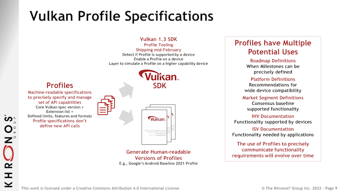
At a high level, profiles are the solution to the widening gap between baseline ES 3.1 hardware, and what current and future hardware can do. Rather than risk fragmenting the Vulkan specification itself (and thus ending up with an OpenGL vs. OpenGL ES redux), profiles allow Vulkan to remain whole while giving various classes and generations of hardware their own common feature sets.
In line with the open and laissez faire nature of the Khronos consortium, profiles are not centrally controlled and can be defined by anyone, be it hardware devs, software devs, potato enthusiasts, or even Khronos itself. Similarly, whether a hardware/platform vendor wants to support a given profile is up to them; if they do, then they will need to make sure they expose the required extensions and formats. So this won’t be as neat and tidy as, say, Direct3D feature levels, but it will still be functional while offering the flexibility the sometimes loose consortium needs.
That said, Khronos’s expectation that we should only see a limited number of widely used profiles, many of which they’ll be involved with in some fashion. So 280 extensions should not become 280 profiles, at least as long as the hardware vendors can find some common ground across their respective platforms.
Finally, on a technical level, it’s worth noting that profiles aren’t just a loose list of features, but they do have technical requirements. Specifically, profiles are built as JSON lists, which along with providing a means to check profile compatibility, also open the door to things like generating human-readable versions of profiles. It’s a small distinction, but it will help developers quickly implement profile support in a generic fashion, relying on the specific JSON lists to guide their programs the rest of the way.
Profiles are also not limited to being built upon Vulkan 1.3. Despite being introduced at the same time as 1.3, they are actually a super-feature of sorts that can work with previous Vulkan versions, as all of the heavy lifting is being done at the application and SDK level. So it will be possible to have a profile that only calls for a Vulkan 1.0 implementation, for example.
Google’s Android Baseline 2021 Profile
The first profile out the door, in turn, comes from Google. The Android author is defining a Vulkan profile for their market that, at a high level, will help to better define and standardize what feature are available on most Android devices.
Interestingly, Google’s profile is built upon Vulkan 1.0, and not a newer version of Vulkan. From what we’re told, there are features in the Vulkan 1.1 core specification that are still not widely supported by mobile devices (even with the ES 3.1 hardware compatibility goal), and as a result, any kind of common progression with Vulkan on Android has become stalled. So since Google can’t get Vulkan 1.1/1.2/1.3 more widely supported across Android devices, the company is doing the next best thing and using a profile to define a bunch of common post-1.0 extensions that are supported by the current crop of devices.
The net result of this is the Android Baseline 2021 Profile. By establishing a baseline profile for the ecosystem, Google is aiming to not only make newer functionality more accessible to developers, but to simplify graphics programming in the process. Essentially, the Baseline 2021 Profile is a fix for existing fragmentation within the Android ecosystem by establishing a reasonable set of commonly supported features and formats.
Of particular note, Google’s profile calls for support for both ETC and ASTC texture compression formats. As well, sample shading and multi-sample interpolation are on the list as well. Given that this is a baseline specification, there aren’t any high-concept next-generation features contained within the profile. But over time, that will change. Google has already indicated that they will be developing a 2022 profile for later this year, and will continue to keep adding further baseline profiles as the situation warrants.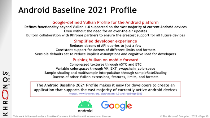
Finally, Google’s use of profiles is also a solid example of taking advantage of the application-centric nature of profiles. According to Google, developers will be able to use profiles on the “vast majority” of Android devices without the need for over-the-air updates for those devices. Since profiles are handled at the application/SDK level, all the device itself needs to present are the necessary Vulkan extensions, which in accordance with a baseline specification are already present and supported in the bulk of Android devices.
Vulkan Roadmap 2022: Making Next-Generation Features Common Features
Last but certainly not least, the other big development to stem from the addition of profiles is a renewed path forward for developing and adopting new features for next-generation hardware. As mentioned previously, Vulkan has until now lacked a way to define feature sets for more advanced (non-core) features, which profiles are finally resolving. As a result, Khronos and the hardware vendors finally have the tools they need to establish baselines for not just low-end hardware, but high-end hardware as well.
In other words, profiles will provide the means to finally create some common standards that incorporate next-generation hardware and the latest programming features.
Because of Vulkan core’s ES 3.1 hardware requirements, there is a significant number of advanced features that have remained optional extensions. This includes everything from ray tracing and sample rate shading to more basic features like anisotropic filtering, multiple processor scheduling, and bindless resources (descriptor indexing). To be sure, these are all features that developers have had access to for years as extensions, but lacking profiles, there has been no assurance for developers that a given feature is going to be in all the platforms they want to target.
To that end, Khronos and its members have developed the Vulkan Roadmap 2022, which is both a roadmap of features they want to become common, as well as a matching profile to go with the roadmap. Conceptually, the Vulkan Roadmap 2022 feature set can be thought of as the inverse of Google’s baseline profile; instead of basing a profile around low-end devices, Roadmap 2022 excises low-end devices entirely in order to focus on common features found in newer hardware.
Roadmap 2022 is being based around features found in mid-end and high-end devices, mobile and PC alike. So while it significantly raises the bar in terms of features supported, it’s still not leaving mobile devices behind entirely – nor would it necessarily be ideal to do so. In practice, this means that Roadmap 2022 is slated to become the common Vulkan feature set for mid-end and better devices across the hardware spectrum.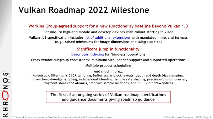
Meanwhile, adoption of Roadmap 2022 should come very quickly since it’s based around features and formats already supported in existing hardware. AMD and NVIDIA have already committed to enabling support for the necessary features in their Vulkan 1.3 drivers, which are out today in beta and should reach maturity in a couple of months. In fact, the biggest hold-up to using profiles is Khronos itself – the Vulkan SDK won’t get profile support until next month.
Finally, according to Khronos Roadmap 2022 is just the start of the roadmapping process for the group. After getting caught-up with current-generation hardware with this year’s profile, the group will be developing longer-term roadmaps for Vulkan profiles. Specifically, the group wants to get far enough ahead of the process that profiles are being planned out years in advance, when the next-generation of hardware is still under development. This would enable Khronos to have a compete pipeline of profiles in the works, giving hardware and software developers a roadmap for the next couple of years of Vulkan features.
Ultimately, having a roadmap will serve to help keep the development of advanced features for Vulkan on-track. Freed from having to support the oldest of hardware, the Vulkan group members will be able to focus on developing and implementing new features, knowing exactly when support is expected/planned/desired to arrive. Up until now the planning process has been weighed down by the lack of a timeline for making new features a requirement (de jure or otherwise), so having a formal process to standardize advanced features will go a long way towards speeding up and simplifying that process.
More...


 Quote
Quote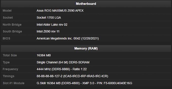
Thread Information
Users Browsing this Thread
There are currently 12 users browsing this thread. (0 members and 12 guests)


Bookmarks