

Results 11,431 to 11,440 of 12091
Thread: Anandtech News
-
02-15-22, 08:14 AM #11431
Anandtech: Intel to Acquire Tower Semiconductor for $5.4B To Expand IFS Capabilities
Continuing their recent spending spree in expanding their foundry capabilities, Intel this morning has announced that it has struck a deal to acquire specialty foundry Tower Semiconductor for $5.4 billion. If approved by shareholders and regulatory authorities, the deal would result in Intel significantly expanding its own contract foundry capabilities, acquiring not only Tower’s various fabs and specialty production lines, but also the company’s experience in operating contract foundries over the long run.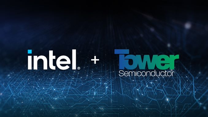
The proposed deal marks the latest venture from Intel that is designed to bolster Intel Foundry Services’ (IFS) production capabilities. In the last month and a half alone, Intel has announced plans to build a $20B fab complex in Ohio that will, in part, be used to fab chips for IFS, as well as a $1B fund to support companies building new and critical technologies for the overall foundry ecosystem. The Tower Semiconductor acquisition, in turn, is yet another piece of the puzzle for IFS, fleshing out Intel’s foundry capabilities for more exotic products.
As a specialty foundry, the Israel-based Tower Semiconductor is best known for its analog offerings, as well as its other specialized process lines. Among the chip types produced by Tower are MEMS, RF CMOS, BiCMOS, CMOS image sensors, silicon–germanium transistors, and power management chips. Essentially, Tower makes most of the exotic chip types that logic-focused Intel does not – so much so that Intel has been a Tower customer long before today’s deal was announced. All of which is why Intel wants the firm and its capabilities: to boost IFS’s ability to make chips for customers who aren’t after a straight ASIC processor.
The proposed acquisition would also see Intel pick up ownership of/access to the 8 foundry facilities that Tower uses. This includes the Tower-owned 150mm and 200mm fabs in Israel and two 200mm fabs in the US. Meanwhile Tower also has majority ownership in two 200mm fabs and a 300mm fab in Japan, and a future 300mm facility in Italy that will be shared with ST Microelectronics. As is typical for analog and other specialty processes where density is not a critical factor (if not a detriment), all of these fabs are based around mature process nodes, ranging from 1000nm down to 65nm, which sits in stark contrast to Intel’s leading-edge logic fabs.
Along with Tower’s manufacturing technology, the proposed deal would also see Intel pick up Tower’s expertise in the contract foundry business, which is something the historically insular Intel lacks. On top of their fab services, Tower also offers its customers electronic design automation and design services using a range of IP, all of which will be folded into IFS’s expanded offerings as part of the deal. Consequently, although the company has already brought on executives and other personnel with contract fab experience in past hirings, this would be the single largest talent transaction for IFS.
All told, Intel currently expects the deal to take around 12 months to close, with the company paying $5.4 billion in cash from its balance sheet for Tower Semiconductor shares. Though approved by both the Intel and Tower Semiconductor boards, Tower’s stockholders will still need to approve the deal. Intel will also need regulatory approval from multiple governments in order to close the deal, to which the company isn’t expecting much objection to given the complementary nature of the two companies’ foundry offerings. Still, as the last week alone has proven, regulatory approval for multi-billion dollar acquisitions is not always guaranteed.
More...
-
02-16-22, 10:58 AM #11432
Anandtech: Ampere Goes Quantum: Get Your Qubits in the Cloud
When we talk about quantum computing, there is always the focus on what the ‘quantum’ part of the solution is. Alongside those qubits is often a set of control circuitry, and classical computing power to help make sense of what the quantum bit does – in this instance, classical computing is our typical day-to-day x86 or Arm or others with ones and zeros, rather than the wave functions of quantum computing. Of course, the drive for working quantum computers has been a tough slog, and to be honest, I’m not 100% convinced it’s going to happen, but that doesn’t mean that companies in the industry aren’t working together for a solution. In this instance, we recently spoke with a quantum computing company called Rigetti, who are working with Ampere Computing who make Arm-based cloud processors called Altra, who are planning to introduce a hybrid quantum/classical solution for the cloud in 2023.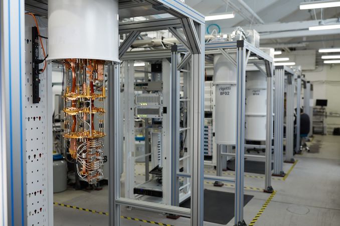
More...
-
02-16-22, 10:58 AM #11433
Anandtech: A Visit to Intels D1X Fab: Next Generation EUV Process Nodes
On a recent trip to the US, I decided to spend some time criss-crossing the nation for a couple of industry events and spend some of the time visiting friends and peers. One of those stops was at Intel’s D1X Fab in Hillsboro, Oregon, one of the company’s leading edge facilities used for both production and development. It’s very rare to get time in a fab as a member of the press – in the ten years covering the industry, I’m lucky to say this was my second, which is usually two more than most. As you can imagine, everything had to be pre-planned and pre-approved, but Intel managed to fit me into their schedule.
More...
-
02-17-22, 02:44 PM #11434
Anandtech: Intel Goes Full XPU: Falcon Shores to Combine x86 and Xe For Supercomputer
One of Intel’s more interesting initiatives over the past few years has been XPU – the idea of using a variety of compute architectures in order to best meet the execution needs of a single workload. In practice, this has led to Intel developing everything from CPUs and GPUs to more specialty hardware like FPGAs and VPUs. All of this hardware, in turn, is overseen at the software level by Intel’s oneAPI software stack, which is designed to abstract away many of the hardware differences to allow easier multi-architecture development.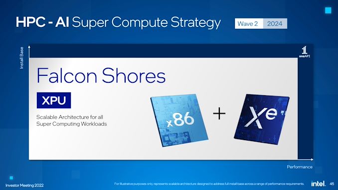
Intel has always indicated that their XPU initiative was just a beginning, and as part of today’s annual investor meeting, Intel is finally disclosing the next step in the evolution of the XPU concept with a new project codenamed Falcon Shores. Aimed at the supercomputing/HPC market, Falcon Shores is a new processor architecture that will combine x86 CPU and Xe GPU hardware into a single Xeon socket chip. And when it is released in 2024, Intel is expecting it to offer better than 5x the performance-per-watt and 5x the memory capacity of their current platforms.
At a very high level, Falcon Shores appears to be an HPC-grade APU/SoC/XPU for servers. While Intel is offering only the barest of details at this time, the company is being upfront in that they are combining x86 CPU and Xe GPU hardware into a single chip, with an eye on leveraging the synergy between the two. And, given the mention of advanced packaging technologies, it’s a safe bet that Intel has something more complex than a monolithic die planned, be it separate CPU/GPU tiles, HBM memory (e.g. Sapphire Rapids), or something else entirely.
Diving a bit deeper, while integrating discrete components often pays benefits over the long run, the nature of the announcement strongly indicates that there’s more to Intel’s plan here than just integrating a CPU and GPU into a single chip (something they already do today in consumer parts). Rather, the presentation from Raja Koduri, Intel’s SVP and GM of the Accelerated Computing Systems and Graphics (AXG) Group, makes it clear that Intel is looking to go after the market for HPC users with absolutely massive datasets – the kind that can’t easily fit into the relatively limited memory capacity of a discrete GPU.
A singular chip, in comparison, would be much better prepared to work from large pools of DDR memory without having to (relatively) slowly shuffle data in and out of VRAM, which remains a drawback of discrete GPUs today. In those cases, even with high speed interfaces like NVLink and AMD’s Infinity Fabric, the latency and bandwidth penalties of going between the CPU and GPU remain quite high compared to the speed at which HPC-class processors can actually manipulate data, so making that link as short as physically possible can potentially offer performance and energy savings.
Meanwhile, Intel is also touting Falcon Shores as offering a flexible ratio between x86 and Xe cores. The devil is in the details here, but at a high level it sounds like the company is looking at offering multiple SKUs with different numbers of cores – likely enabled by varying the number of x86 and Xe titles.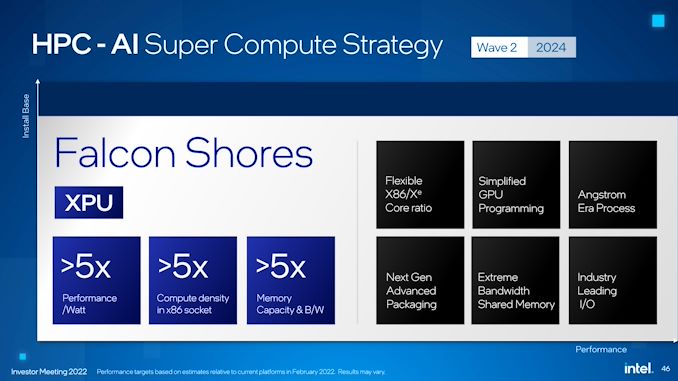
From a hardware perspective then, Intel seems to be planning to throw most of their next-generation technologies at Falcon Shores, which is fitting for its supercomputing target market. The chip is slated to be built on an “angstrom era process”, which given the 2024 date is likely Intel’s 20A process. And along with future x86/Xe cores, will also incorporate what Intel is calling “extreme bandwidth shared memory”.
With all of that tech underpinning Falcon Shores, Intel is currently projecting a 5x increase over their current-generation products in several metrics. This includes a 5x increase in performance-per-watt, a 5x increase in compute density for a single (Xeon) socket, a 5x increase in memory capacity, and a 5x increase in memory bandwidth. In short, the company has high expectations for the performance of Falcon Shores, which is fitting given the highly competitive HPC market it’s slated for.
And perhaps most interestingly of all, to get that performance Intel isn’t just tackling things from the raw hardware throughput side of matters. The Falcon Shores announcement also mentions that developers will have access to a "vastly simplified GPU programming model" for the chip, indicating that Intel isn’t just slapping some Xe cores into the chip and calling it a day. Just what this entails remains to be seen, but simplifying GPU programming remains a major goal in the GPU computing industry, especially for heterogeneous processors that combine CPU and GPU processing. Making it easier to program these high throughput chips not only makes them more accessible to developers, but reducing/eliminating synchronization and data preparation requirements can also go a long way towards improving performance.
Like everything else being announced as part of today’s investor meeting, this announcement is more of a teaser for Intel. So expect to hear a lot more about Falcon Shores over the next couple of years as Intel continues their work to bringing it to market.
More...
-
02-17-22, 02:44 PM #11435
Anandtech: Intels Arctic Sound-M Server Accelerator To Land Mid-2022 With Hardware A
Rounding out Intel’s direct GPU-related announcements from this morning as part of the company’s annual investor meeting, Intel has confirmed that the company is also getting ready to deliver a more traditional GPU-based accelerator card for server use a bit later this year. Dubbed Arctic Sound-M, the forthcoming accelerator is being aimed in particular at the media encoding and analytics market, with Intel planning to take full advantage of what should be the first server accelerator with hardware AV1 video encoding. Arctic Sound-M is expected to launch in the middle of this.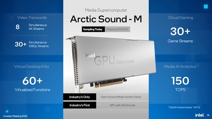
The announcement of Arctic Sound-M follows a hectic, and ultimately sidetracked set of plans for Intel’s original GPU server hardware. The company initially commissioned their Xe-HP series of GPUs to anchor the traditional server market, but Xe-HP was canceled in November of last year. Intel didn’t give up on the server market, but outside of the unique Ponte Vecchio design for the HPC market, they did back away from using quite so much dedicated server silicon.
In the place of those original products, which were codenamed Arctic Sound, Intel is instead coming to market with Arctic Sound-M. Given the investor-focused nature of today’s presentation, Intel is not publishing much in the way of technical details for their forthcoming server accelerator, but we can infer from their teaser videos that this is an Alchemist (Xe-HPC part), as we can clearly see the larger Alchemist die mounted on a single-slot card in Intel’s teaser video. This is consistent with the Xe-HP cancellation announcement, as at the time, Intel’s GPU frontman, Raja Koduri indicated that we’d see server products based on Xe-HPG instead.
Arctic Sound-M, in turn, is being positioned as a server accelerator card for the media market, with Intel calling it a “media and analytics supercomputer”. Accordingly, Intel is placing especially heavy emphasis on the media processing capabilities of the card, both in regards to total throughput and in codecs supported. In particular, Intel expects that Arctic Sound-M will be the first accelerator card released with hardware AV1 encoding support, giving the company an edge with bandwidth-sensitive customers who are ready to use the next-generation video codec.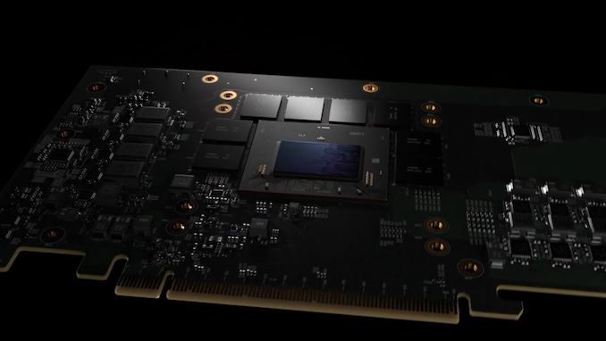
Interestingly, this also implies that hardware AV1 encoding is a native feature of (at least) the large Alchemist die. Though given the potential value of the first hardware AV1 encoder, it remains to be seen whether Intel will enable it on their consumer Arc cards, or leave it restricted to their server card.
Meanwhile in terms of compute performance for media analytics/AI inference, Intel is quoting a figure of 150 TOPS for INT8. There aren’t a ton of great comparisons here in terms of competing hardware, but the closest comparison in terms of card size and use cases would be NVIDIA’s A2 accelerator, where on paper, the Arctic Sound-M would deliver almost 4x the inference performance. It goes without saying that the proof is in the pudding for a new product like Intel’s GPUs, but if they can deliver on these performance figures, then Arctic Sound-M would be able to safely occupy a very specific niche in the larger server accelerator marketplace.
Past that, like the rest of Intel’s Arc(tic) products, expect to hear more details a bit later this year.
More...
-
02-17-22, 07:33 PM #11436
Anandtech: Intel Discloses Multi-Generation Xeon Scalable Roadmap: New E-Core Only Xe
It’s no secret that Intel’s enterprise processor platform has been stretched in recent generations. Compared to the competition, Intel is chasing its multi-die strategy while relying on a manufacturing platform that hasn’t offered the best in the market. That being said, Intel is quoting more shipments of its latest Xeon products in December than AMD shipped in all of 2021, and the company is launching the next generation Sapphire Rapids Xeon Scalable platform later in 2022. Beyond Sapphire Rapids has been somewhat under the hood, with minor leaks here and there, but today Intel is lifting the lid on that roadmap.
More...
-
02-18-22, 08:24 AM #11437
Anandtech: AnandTech Interview with Dr. Ann Kelleher: EVP and GM of Intels Technolog
It’s somewhat of an understatement to say that Intel’s future roadmap on its process node development is one of the most aggressive in the history of semiconductor design. The company is promising to pump out process nodes quicker than we’ve ever seen, despite having gone through a recent development struggle. Even with CEO Pat Gelsinger promising more than ever before, it’s up to Intel’s Technology Development (TD) team to pick up the ball and run with it in innovative ways to make that happen. In charge of it all is Dr. Ann Kelleher, EVP and GM of Intel’s Technology Development, and on the back of some strong announcements last year we reached out for the chance to interview her regarding Intel’s strategy.
More...
-
02-18-22, 05:42 PM #11438
Anandtech: EVGA Unleashes Z690 Dark K|NGP|N Edition Motherboard: Alder Lake Goes Extr
Although these long, cold, and dark nights are starting to come to an end, EVGA has launched its darkest and most devilish desktop motherboard to date, the EVGA Z690 Dark K|NGP|N Edition. Designed in collaboration with legendary extreme overclocker Vince 'K|NGP|N' Lucido, the Z690 Dark K|NGP|N Edition boasts an impressive feature set including support for DDR5-6600 memory, three PCIe 4.0 x4 M.2 slots, eight SATA ports, and a large 21-phase power delivery to push Intel's Alder Lake to the extreme.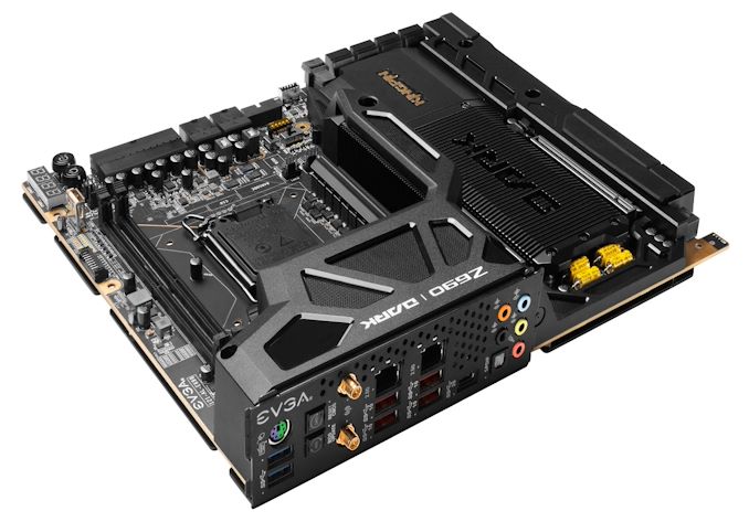
Built around the Intel's high-end Z690 chipset, the EVGA Z690 Dark K|NGP|N Edition isn't a conventional motherboard by any stretch of the imagination. It is based on the E-ATX form factor and has interesting design characteristics, including a transposed LGA1700 socket that allows extreme overclockers to mount LN2 pots more easily.
To make the board more robust, EVGA includes a large black metal backplate on the rear of the board to reinforce the PCB. This also includes right-angled connectors, including two 8-pin 12V ATX CPU power inputs and a 24-pin 12V ATX motherboard power input that intrudes into the PCB with a handy cutout designed to make cable management more effortless. It also includes an impressive accessories pack that features an EVGA flat test bench plate that we saw in our previous review of the EVGA Z590 Dark motherboard.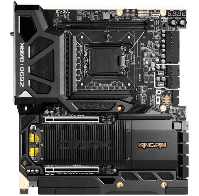
Looking at the feature set, the Z690 Dark K|NGP|N Edition includes two full-length PCIe 5.0 slots that can operate at x16 and x8/x8, with three PCIe 4.0 x4 M.2 slots that sit in between the PCIe slots and underneath a large black finned 'Dark' branded heatsink. There are eight SATA ports for conventional storage and optical drives, six of which are from the chipset with RAID 0, 1, 5, and 10 support, and two that come via an ASMedia ASM1061 SATA controller.
Even though the Z690 Dark has a solid feature set for enthusiasts, the real focus by EVGA with this model is on extreme overclocking. This includes a large 21-phase power delivery cooled by an active heatsink with two fans. It also has a 10-layer PCB throughout and contains an overclocker's toolkit in the top right-hand corner that consists of dual two-digit LED debuggers, a power button, a reset button, dip-switches to disable PCIe slots, and a slow mode switch. There's also a probe-lt header where users can monitor voltages in real-time from various components on the board, such as the CPU and power inputs.
In terms of connectivity, there's plenty on the rear panel, including one USB 3.2 G2x2 Type-C, four USB 3.2 G2 Type-A, and two USB 3.2 G1 Type-A ports. For networking, EVGA uses two Intel I225-V 2.5 GbE controllers and includes Intel's latest AX211 Wi-Fi 6E CNVi. Despite focusing on performance, EVGA has also gone with a premium audio solution, including a Realtek ALC1220 HD audio codec and an EVGA NU Audio SV3H615 headphone amplifier with five 3.5 mm audio jacks and a single S/PDIF optical output.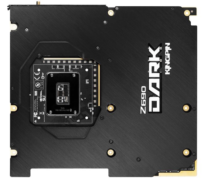
The large black metal backplate on the rear of the EVGA Z690 Dark K|NGP|N Edition
The EVGA Z690 Dark K|NGP|N Edition is currently available to purchase at the EVGA website for $830. However, at the time of writing, purchases are limited to one per household, and it seems as though it's only available to EVGA Elite Members at this time.
Gallery: EVGA Unleases Z690 Dark K|NGP|N Edition Motherboard, Alder Lake Goes Extreme


Source: EVGA
Related Reading- The MSI MEG Z690 Unify (DDR5) Motherboard Review: The All-Black Option
- CES 2022: ASRock Unveils Z690 Aqua and Z690 Aqua OC Motherboards
- The Intel Z690 Motherboard Overview (DDR5): Over 50+ New Models
- The Intel Z690 Motherboard Overview (DDR4): Over 30+ New Models
More...
-
02-18-22, 05:42 PM #11439
Anandtech: From There to Here, and Beyond
I’ll be the first to admit, I had no history with AnandTech before I joined. It was by sheer chance, meeting one of the writers at an overclocking event, that led me to first become a reader, then a writer, to what has become my career in journalism. If you’re new to AnandTech then welcome! It’s been my home for over a decade, where we’ve always had the goal of pushing the boundaries for all things technical and engineering-related. For all the old hands - I know many of you work at the companies we report on around the industry, and we’ve been forever glad for your continued support and interactions. Long may it continue, especially in an industry that is slowly consolidating around a few key players, both in technical and publishing – for as long as the audience demands it, AnandTech will aim to provide.
Personally, I was always into computers, but it was overclocking that got me into hardware. Not just getting more frames in my games, but actual competitive overclocking, trying to get the best scores in the world. People liken it to the Formula 1 or car tuning, when in reality it feels like drag racing – 8 hours of preparation for a 10 seconds quarter mile. Studying chemistry at the time, on the surface there seemed to be not much more than a little overlap, except for a desire to learn more about what I was doing, the why, and how it all worked. That oblivious-yet-determined manner led to Rajinder Gill, senior motherboard editor at the time, suggesting that Anand bring me on as a freelancer back in 2010. Initially with news, I transitioned into Rajinder’s role rather quickly after he left, and starting from the Sandy Bridge launch in early 2011, I spent the next five years reviewing motherboards at AnandTech as my day job after graduating my PhD. I still look back on my first proper motherboard review, the ASRock P67 Extreme4, with rose-tinted spectacles. It was a great board for the time, and I still have it in my collection.
That’s what got me to AnandTech, and after 11 years I feel the need to change, so I have decided to take up a new position in the industry. When Anand left in 2014, after 18 years at the helm, I was still quite green in my role and didn’t really take his words to heart at the time. Looking back at them today, I see a lot of parallels, even though I’ve never sat in that senior role. Since Anand left, I was promoted to Senior CPU Editor, and Ryan Smith has taken the Editor-in-Chief role with grace and poise – he’s consistently talked me down from a ledge when this industry has piled on, and all I’ve wanted to do is lash out! After Anand left, it was Ryan who brought me on as a full-time employee, and helped navigate AnandTech through two acquisitions, to where the brand currently sits today with Future. Despite being (roughly) the same age, Ryan has been a mentor and a director for a lot of the content I’ve written, for which I’m very thankful. I hope he knows how much it has meant over the years.
I’ve really enjoyed working at AnandTech. I love getting my teeth into the latest technical details, and getting advance briefings from the researchers never ceases to be a great pleasure of mine. It doesn’t matter whether that’s for an upcoming product, attending technical IEEE conferences, or for Hot Chips talk, or seeing inside the secret R&D room at Computex. In a lot of ways, my academic experience has overlapped with my coverage that I would never have predicted - we're on the cusp of finding out how we need More Than Moore's Law in the modern era. My travel in 2019 topped 200,000 miles, which doesn’t really bother me in the slightest, as I’ve been able to meet and discuss with key industry movers and shakers. A crowning moment was talking AMD into making its 64-core Threadripper into a better price the evening before the announcement. Or biting one of Intel’s 10nm wafers. Being able to travel around and visit companies has shown me just how many amazing people and stories there are in our industry, and it’s a shame there aren’t enough hours in the day to focus on them all, as I know a lot of you would want to hear about them. I hope I've also been able to bring a little bit of humor and fun to my content too.
If there’s one thing that has remained through all that time, it’s the dedication of AnandTech’s writers to provide as many detailed technical write-ups as we can. Over the years I’ve worked with some incredible talent, especially Andrei, and I’ve managed individuals that I’ve seen improve leaps and bounds, especially Gavin who now leads our motherboard coverage. Big shoutouts go to the rest of the team over the years: Ryan, Brett, Ganesh, Billy, Kristian, Tracy, Anton, Joe, Matt, Matt, Josh, Nate, Rajinder, Gary, Virginia, and Howard. You’ve all meant a lot to me in so many different ways. Then there’s also the audience, who have always provided copious feedback, either here, on social media, or through our email conversations. Please don’t stop giving all of us constructive criticism on how to do our jobs better, regardless of where we are or who we work for.
As for me, I’m finding new ventures: a mixture of behind-the-scenes and public-facing opportunities, as well as continued consulting, but still within this tech industry that we love to analyze. We're on the cusp of finding out how we need More Than Moore's Law in the modern era. I’ll still be that loud voice on Twitter, criticizing every financial disclosure and presentation, and if you’re interested in what I’m doing next, then I’m likely to announce my future roles over there or on LinkedIn in short course. While today is my final day at AnandTech, don't be surprised if my name pops up again here over the next week or two, as I’ve prepared some content in advance, including our AMD Rembrandt review and an interview with Raja Koduri. Stay tuned for those.
To all of the readers over the years, thank you so much for this opportunity. I couldn’t have done it without you. I hope that you’ll continue to give all the AnandTech writers the support you have shown me.
~Ian
More...
-
02-22-22, 03:29 PM #11440
Anandtech: Netgear Launches WAX630E AX7800 Wi-Fi 6E Access Point for SMBs
Netgear has been building up a portfolio of software-defined networking (SDN) products over the last few years. The introduction of the cloud-based Insight management feature to their lineup of SMB products has made their lineup of routers, switches, and access points appeal to a wider customer base. SMB-focused versions of leading technologies often lag their consumer counterparts by a year or so, and updates to flagship offerings are often spaced apart. However, Netgear's Wi-Fi 6 WAX630 (introduced in June 2021) is receiving a Wi-Fi 6E upgrade / companion today in the form of the WAX630E.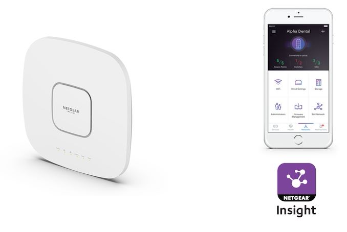
The Qualcomm-based WAX630E is one of the first reasonably-priced SMB Wi-Fi 6E APs for SMBs and micro-businesses. Many announced and leaked offerings in the Wi-Fi 6E space have been delayed (with FCC certification being a stumbling block), allowing Netgear's offering to become available for purchase ahead of the competition. The advantages of Wi-Fi 6E have been covered in multiple articles previously - including the original Wi-Fi Alliance announcement coverage, and Netgear's first Wi-Fi 6E product in the consumer space last year. The availability of a much wider interference-free spectrum in 6 GHz - up to seven usable 160 MHz - means that consumer experience is bound to be much better. The downside is the reduced range due to power limitations (APs at 30 dBm max., and clients at 24 dBm max.).
On the technical front, the WAX630E replaces the third 4x4 5GHz band of the WAX630 with a 2x2 6GHz radio. The 2.4 GHz radio configuration has also been reduced to 2x2 in the WAX630E from the 4x4 in the WAX630. These updates have allowed Netgear to price the WAX630E very competitively at $350 - a reasonable premium of $20 over the WAX630's $330. The reduced number of radios also allows the WAX630E to sport lower maximum power consumption compared to the WAX630 (27.6W vs. 30.1W). However, the availability of 160MHz channels enables the AP to be marketed as an AX7800 device (600 Mbps for the 2x2 2.4 GHz, 4800 Mbps for the 4x4 5 GHz, and 2400 Mbps for the 2x2 6 GHz radios). The AP has a 3000 sq. ft. coverage area. The WAX630E retains the same physical footprint as the WAX630, though it is slight heavier.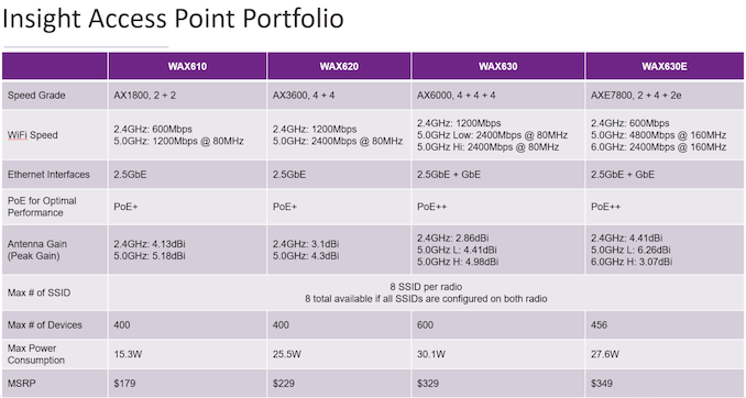
The AP supports PoE++ over the 2.5GbE LAN port (an extra 1Gbps LAN port is also available). Netgear recommends the Insight-managed MS510TXUP NBASE-T PoE++ switch for use with the WAX630E. The introduction of the new AP provides a wider range of options for Netgear's customers, whose needs with respect to required number of clients and client types to support, speeds, and pricing may vary.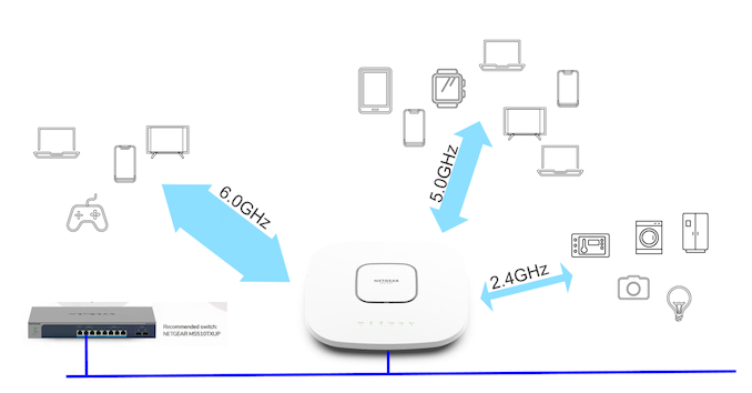
Netgear believes that cloud-based management of Wi-Fi 6E APs will be a must in the long-run. Outdoor APs will eventually need to figure out a solution for ensuring that they do not interfere with other licensed 6 GHz band users. FCC mandates that real-time geolocation database cross-checks need to be performed by APs, which might be a challenge without regular updates to the database. While the WAX630E is not affected by this (due to its indoor nature), cloud-based management / real-time connection to a database maintained by the vendor might become essential moving forward. Netgear's Insight provides IT administrators with a centralized dashboard for multi-location installations, allowing for both local and remote management. Netgear is touting scalability and easy-to-use multi-location support as advantages over solutions requiring local controllers.
The WAX630E is available for pre-order today - $350 for the PoE variant, and $370 for the one with a power adapter included. The units are expected to ship early next month.
Gallery: Netgear Launches WAX630E AX7800 Wi-Fi 6E Access Point for SMBs


More...


 Quote
QuoteThread Information
Users Browsing this Thread
There are currently 14 users browsing this thread. (0 members and 14 guests)


Bookmarks