

Results 11,511 to 11,520 of 12091
Thread: Anandtech News
-
06-06-22, 11:29 AM #11511
Anandtech: The Apple WWDC 2022 Keynote Live Blog (Starts at 10am PT/17:00 UTC)
As we round the corner after Computex and transition into June, it's time once more for Apple's annual World Wide Developers Conference. As always, Apple kicks off WWDC with their big keynote event, which though aimed first and foremost at developers, is also used as a venue to announce new products and ecosystem strategies. The keynote starts at 10am Pacific (17:00 UTC) today, and AnandTech will be offering live blog coverage of Apple's event.
With WWDC going virtual once again this year, we're expecting another rapid-fire, two-hour run through of Apple's ecosystem. WWDC keynotes have historically covered everything from macOS and iOS to individual Apple applications and more. On the hardware side of matters, in previous years we've seen things like the official announcement of Apple's shift from x86 to Apple Silicon; and while 2021 was light on hardware, one never quite knows what Apple has in store. Apple has yet to launch an Arm-based Mac Pro, so there's still some big surprises left in their bag, and of course there's always the chance of the periodic product refresh.
So join us at 10am Pacific to see just what Apple is working on for this year and beyond.
More...
-
06-06-22, 06:42 PM #11512
Anandtech: Apple Announces M2 SoC: Apple Silicon for Macs Updated For 2022
Though primarily a software-focused event, Apple’s WWDC keynotes are often stage for an interesting hardware announcement or two as well, and this year Apple did not disappoint. At the company’s biggest Mac-related keynote of the year, Apple unveiled the M2, their second-generation Apple Silicon SoC for the Mac (and iPad) platform. Touting modest performance gains over the original M1 SoC of around 18% for multithreaded CPU workloads and 35% in peak GPU workloads, the M2 is Apple’s first chance to iterate on their Mac SoC to incorporate updated technologies, as well as to refresh their lower-tier laptops in the face of recent updates from their competitors.
With the king of the M1 SoCs, M1 Ultra, not even 3 months behind them, Apple hasn’t wasted any time in preparing their second generation of Apple Silicon SoCs. To that end, the company has prepared what is the first (and undoubtedly not the last) of a new family of SoCs with the Apple Silicon M2. Designed to replace the M1 within Apple’s product lineup, the M2 SoC is being initially rolled out in refreshes of the 13-inch MacBook Pro, as well as the MacBook Air – which is getting a pretty hefty redesign of its own in the process.
The launch of the M2 also gives us our first real glimpse into how Apple is going to handle updates within the Apple Silicon ecosystem. With the iPhone family, Apple has kept to a yearly cadence for A-series SoC updates; conversely, the traditional PC ecosystem is on something closer to a 2-year cadence as of late. M2 seems to split this down the middle, coming about a year and a half after the M1 – though in terms of architecture it looks closer to a yearly A-series SoC update.
More...
-
06-08-22, 12:54 PM #11513
Anandtech: Supermicro SYS-E100-12T-H Review: Fanless Tiger Lake for Embedded Applicat
Compact passively-cooled systems find application in a wide variety of market segments including industrial automation, IoT gateways, digital signage, etc. These are meant to be deployed for 24x7 operation in challenging environmental conditions. Supermicro has a number of systems targeting this market under the Embedded/IoT category. Their SuperServer E100 product line makes use of motherboards in the 3.5" SBC form-factor. In particular, the E100-12T lineup makes use of embedded Tiger Lake-U SoCs to create powerful, yet compact and fanless systems. Today's review takes a look at the top-end of this line - the SYS-E100-12T-H based on the Intel Core i7-1185GRE embedded processor.
More...
-
06-09-22, 06:05 PM #11514
Anandtech: AMD's Desktop CPU Roadmap: 2024 Brings Zen 5-based "Granite Ridge"
As part of AMD's Financial Analyst Day 2022, it has provided us with a look at the company's desktop client CPU roadmap as we advance towards 2024. As we already know, AMD's latest 5 nm chips based on its Ryzen 7000 family are expected to launch in Fall 2022 (later this year), but the big news is that AMD has confirmed their Zen 5 architecture will be coming to client desktops sometime before the end of 2024 as AMD's "Granite Ridge" chips.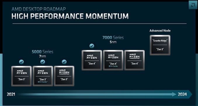
At Computex 2022, during AMD's Keynote presented by CEO Dr. Lisa Su, AMD unveiled its Zen 4 core architecture using TSMC's 5 nm process node. Despite not announcing specific SKUs during this event, AMD did unveil some expected performance metrics that we could expect to see with the release of Ryzen 7000 for desktop. This includes 1 MB per core L2 cache, which is double the L2 cache per core with Zen 3, and up to a 15% performance uplight in single-threaded IPC performance.
AMD 3D V-Cache Coming to Ryzen 7000 and Beyond
One key thing to note with AMD's updated client CPU roadmap, it highlights some more on what to expect with its Zen 4 core, which is built on TSMC's 5 nm node. AMD is expecting 8-10% IPC gains over Zen 3, on top of their previously announced clockspeed gains. As a result, the company is expecting single-threaded performance to improve by at least 15%, and by even more for multi-threaded workloads.
Meanwhile AMD's 3D V-Cache packaging technology will also come to client desktop Zen 4. AMD is holding any further information close to their chest, but their current roadmap makes it clear that we should, at a minimum, expect a successor to the the Ryzen 7 5800X3D.
AMD Zen 5 For Client Desktop: Granite Ridge
The updated AMD client CPU roadmap until 2024 also gives us a time frame of when we can expect its next-generation Zen 5 cores. Built on what AMD is terming an "advanced node" (so either 4 nm or 3 nm), Zen 5 for client desktops will be Granite Ridge.
At two years out, AMD isn't offering any further details than what they've said about the overall Zen 5 architecture thus far. So while we know that Zen 5 will involve a significant reworking of AMD's CPU architecture with a focus on the front end and issue width, AMD isn't sharing anything about the Granite Ridge family or related platform in particular. So sockets, chipsets, etc are all up in the air.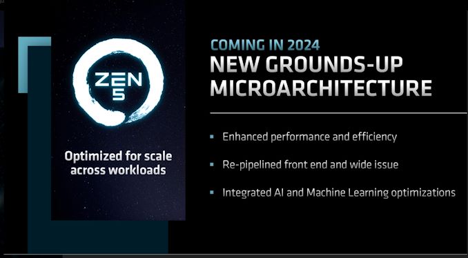
But for now, AMD's full focus is on the Zen 4-based Ryzen 7000 family. Set to launch this fall, 2022 should end on a high note for the company.

More...
-
06-09-22, 06:05 PM #11515
Anandtech: Updated AMD Notebook Roadmap: Zen 4 on 4nm in 2023, Zen 5 By End of 2024
As we've come to expect during AMD's Financial Analyst Day (FAD), we usually get small announcements about big things coming in the future. This includes updated product roadmaps for different segments such as desktop, server, graphics, and mobile. In AMD's latest notebook roadmap stretching out to 2024, AMD has unveiled that its mobile Zen 4 core (Pheonix Point) will be available sometime in 2023 and Zen 5 for mobile on an unspecified node which is expected to land sometime by the end of 2024.
The updated AMD Notebook roadmap through to 2024 highlights two already available mobile processors, the Zen 3-based Ryzen 5000 series with Vega integrated graphics and the latest Ryzen 6000 based on Zen 3+ and with the newest RDNA 2 mobile graphics capabilities. But there's more that is due to be announced starting in 2023.
From The Rembrandt, Rises a Pheonix: Zen 4 Mobile AKA Pheonix Point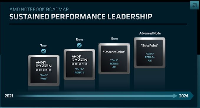
What's new and upcoming on the updated AMD mobile roadmap is the successor to Rembrandt (Ryzen 6000), which AMD has codenamed Pheonix Point. AMD Phenoix Point will be based on AMD's upcoming Zen 4 core architecture and will be built using TSMC's 4 nm process node. According to the roadmap, AMD's Zen 4 Pheonix Point mobile processors will use Artificial Intelligence Engine (AIE) and AMD's upcoming and next-generation RDNA 3 integrated graphics. It's unclear whether the platform will use DDR5 or DDR4 memory, but seeing as how Ryzen 7000 (Zen 4) uses the same core architecture and will be exclusive to DDR5 only that Pheonix Point will use DDR5 memory.
Also Announced: Zen 5 Mobile Codenamed Strix Point
Also on the AMD notebook roadmap is the announcement of its Zen 5-based platform on an unspecified manufacturing process, codenamed Strix Point. While details on Strix Point are minimal, AMD does state that Strix Point will use AMD's unreleased RDNA 3+ graphics technology, which will likely be a refreshed and perhaps more performance per watt efficient RDNA 3 variation.
Also listed within the slide of the roadmap with Pheonix Point and Strix Point is an Artificial Intelligence Engine (AIE), which is more commonly found in mobile phones. The AI Engine or AIE will allow AMD to spec its products based on tiling with an adaptive interconnect. Still, it hasn't unveiled much more about how it intends to incorporate AIE into its notebook portfolio. We know that it is part of AMD's XDNA Adaptive Architecture IP, which comes from its acquisition of Xilinx.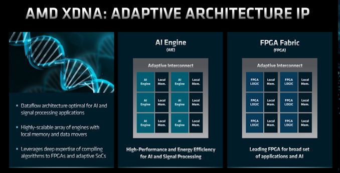
We will likely learn more about AMD's Pheonix Point based on Zen 4 in the coming future, as a release date sometime in 2023 is expected. As for Strix Point, which will be using its unannounced Zen 5 microarchitecture, we're likely to hear more about this next year sometime.
More...
-
06-13-22, 06:16 AM #11516
Anandtech: Intel 4 Process Node In Detail: 2x Density Scaling, 20% Improved Performan
Taking place this week is the IEEE’s annual VLSI Symposium, one of the industry’s major events for disclosing and discussing new chip manufacturing techniques. One of the most anticipated presentations scheduled this year is from Intel, who is at the show to outline the physical and performance characteristics of their upcoming Intel 4 process, which will be used for products set to be released in 2023. The development of the Intel 4 process represents a critical milestone for Intel, as it’s the first Intel process to incorporate EUV, and it’s the first process to move past their troubled 10nm node – making it Intel’s first chance to get back on track to re-attaining fab supremacy.
Intel’s scheduled to deliver their Intel 4 presentation on Tuesday, in a talk/paper entitled “Intel 4 CMOS Technology Featuring Advanced FinFET Transistors optimized for High Density and High-Performance Computing”. But this morning, ahead of the show, they re publishing the paper and all of its relevant figures, giving us our first look at what kind of geometries Intel is attaining, as well as some more information about the materials being used.
More...
-
06-15-22, 07:36 AM #11517
Anandtech: The ASUS ROG Maximus Z690 Hero Motherboard Review: A Solid Option For Alde
Over the last six months since Intel launched its 12th Gen Core series of processors, we've looked at several Alder Lake desktop CPUs and seen how competitive they are from top to bottom - not just in performance but price too. To harness the power of Alder Lake, however, there are many options in terms of Z690 motherboards, and today we're taking a look at one of ASUS's more premium models, the ROG Maximus Z690 Hero.
They say hard times don't create heroes, but ASUS has done for many years with good results. Equipped with plenty of top-tier features such as Thunderbolt 4, Intel's Wi-Fi 6E CNVi, and support for up to DDR5-6400 memory, it has enough to make it a solid choice for gamers and enthusiasts. It's time to see if the Z690 Hero option stacks up against the competition and if it can sparkle in a very competitive LGA1700 market.
More...
-
06-16-22, 03:12 PM #11518
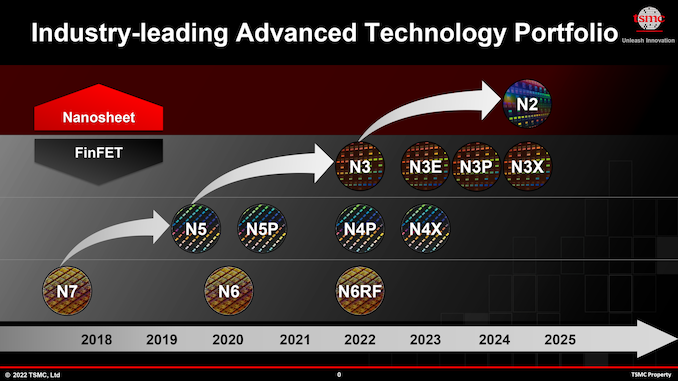
Anandtech: TSMC Unveils N2 Process Node: Nanosheet-based GAAFETs Bring Significant Be
At its 2022 Technology Symposium, TSMC formally unveiled its N2 (2 nm class) fabrication technology, which is slated to go into production some time in 2025 and will be TSMC's first node to use gate-all-around field-effect transistors (GAAFETs). The new node will enable chip designers to significantly reduce the power consumption of their products, but the speed and transistor density improvements seem considerably less tangible.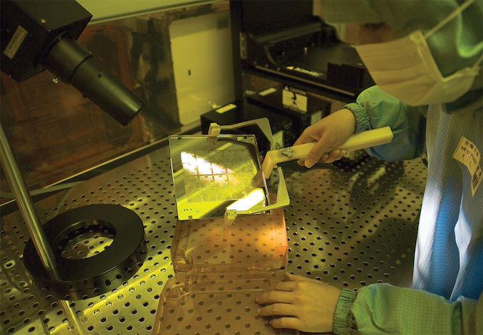
TSMC's N2 is a brand-new platform that extensively uses EUV lithography and introduces GAAFETs (which TSMC calls nanosheet transistors) as well as backside power delivery. The new gate-all-around transistor structure promises well-published advantages, such as greatly reduced leakage current (now that the gates are around all four sides of the channel) as well as ability to adjust channel width to increase performance or lower power consumption. As for the backside power rail, it is generally designed to enable better power delivery to transistors, offering a solution to the problem of increasing resistances in the back-end-of-line (BEOL). The new power delivery is slated to increase transistor performance and lower power consumption.
From feature set standpoint, TSMC's N2 looks like a very promising technology. As for actual numbers, TSMC promises that N2 will allow chip designers to increase performance by 10% to 15% at the same power and transistor count, or reduce power consumption at the same frequency and complexity by 25% ~ 30%, all the while increasing chip density by over 1.1-fold when compared to N3E node.
*Chip density published by TSMC reflects 'mixed' chip density consisting of 50% logic, 30% SRAM, and 20% analog.Advertised PPA Improvements of New Process Technologies
Data announced during conference calls, events, press briefings and press releasesTSMC N5
vs
N7N3
vs
N5N3EvsN5N2
vs
N3EPower -30% -25-30% -34% -25-30% Performance +15% +10-15% +18% +10-15% Chip Density* ? ? ~1.3X >1.1X Volume
ManufacturingQ2 2022 H2 2022 Q2/Q3 2023 H2 2025
Versus N3E, the performance improvements and power reductions enabled by TSMC's N2 node are in line with what the foundry's new nodes typically bring in. But the so-called chip density improvements (which should reflect transistor density gains) are just a little over 10%, which is not particularly inspiring, especially considering that N3E already offers a slightly lower transistor density when compared to vanilla N3. Keeping in mind that SRAM and analog circuits barely scale these days, mediocre improvements in transistor density of actual chips should probably be expected these days. However, a chip density improvement of 10% in about three years is certainly not great news for GPUs and other chips that live or die based on rapidly increasing their transistor counts.
Bearing in mind that by the time TSMC's N2 enters production the company will also have the density-optimized N3S node, it would appear that the foundry will have two process technologies based on different types of transistors yet offering very similar transistor densities, something that has never happened before.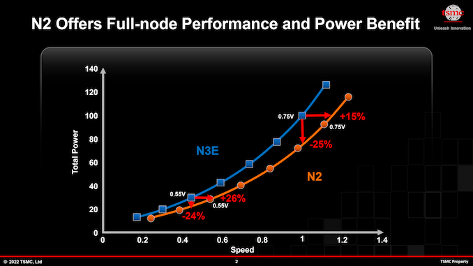
As usual, TSMC will offer their N2 node with various features and knobs to allow chip designers to optimize for things like mobile and high-performance computing designs (note that TSMC calls HPC everything that is not mobile, automotive or specialty. which includes everything from a low-power laptop CPU to a high-end compute GPU aimed at supercomputers). Also, platform offerings include something that TSMC calls 'chiplet integration', which probably means that TSMC enable its customers to easily integrate N2 chips into multi-chiplet packages made using various nodes. Since transistor density scaling is slowing down and new process technologies are getting more expensive to use, multi-chiplet packages are going to become more common in the coming years as developers will be using them to optimize their designs and costs.
TSMC expects to start risk production of chips using its N2 fabrication process sometimes in the second half of 2024, which means that the technology should be available for high volume manufacturing (HVM) of commercial products in the second half of 2025. But, considering the length of modern semiconductor production cycles, it's likely more pragmatic to expect the first N2 chips to become available either very late in 2025 or 2026, if everything goes as planned.
More...
-
06-16-22, 03:12 PM #11519
Anandtech: TSMC Readies Five 3nm Process Technologies, Adds FinFlex For Design Flexib
Taiwan Semiconductor Manufacturing Co. on Thursday kicked off its 2022 TSMC Technology Symposium, where the company traditionally shares it process technology roadmaps as well as its future expansion plans. One of the key things that TSMC is announcing today are its leading-edge nodes that belong to its N3 (3 nm class) and N2 (2nm class) families that will be used to make advanced CPUs, GPUs, and SoCs in the coming years.
N3: Five Nodes Over Next Three Years
As fabrication processes get more complex, their pathfinding, research, and development times get stretched out as well, so we no longer see a brand-new node emerging every two years from TSMC and other foundries. With N3, TSMC's new node introduction cadence is going to expand to around 2.5 years, whereas with N2, it will stretch to around three years.
This means that TSMC will need to offer enhanced versions of N3 in order to meet the needs of its customers who are still looking for a performance per watt improvement as well as transistor density bump every year or so. Another reason why TSMC and its customers need multiple versions of N3 is because the foundry's N2 relies on all-new gate-all-around field-effect transistors (GAA FETs) implemented using nanosheets, which is expected to come with higher costs, new design methodologies, new IP, and many other changes. While developers of bleeding-edge chips will be quick to jump to N2, many of TSMC's more rank & file customers will stick to various N3 technologies for years to come.
At its TSMC Technology Symposium 2022, the foundry talked about four N3-derived fabrication processes (for a total of five 3 nm-class nodes) — N3E, N3P, N3S, and N3X — set to be introduced over the coming years. These N3 variants are slated to deliver improved process windows, higher performance, increased transistor densities, and augmented voltages for ultra-high-performance applications. All these technologies will support FinFlex, a TSMC "secret sauce" feature that greatly enhances their design flexibility and allows chip designers to precisely optimize performance, power consumption, and costs.
*Note that TSMC only started to publish transistor density enhancements for analog, logic, and SRAM separately around 2020. Some of the numbers still reflect 'mixed' density consisting of 50% logic, 30% SRAM, and 20% analog.Advertised PPA Improvements of New Process Technologies
Data announced during conference calls, events, press briefings and press releasesTSMC N4
vs
N5N4P
vs
N5N4P
vs
N4N4X
vs
N5N4X
vs
N4PN3
vs
N5N3E
vs
N5Power lower -22% - ? ? -25-30% -34% Performance higher +11% +6% +15%
or
more+4%
or more+10-15% +18% Logic Area
Reduction* %
Logic Density*0.94x
-6%
1.06x0.94x
-6%
1.06x
-
?
?0.58x
-42%
1.7x0.625x
-37.5%
1.6xVolume
Manufacturing2022 2023 H2 2022 2023 2023 H2 2022 Q2/Q3 2023
N3 and N3E: On Track for HVM
TSMC's first 3 nm-class node is called N3 and this one is on track to start high volume manufacturing (HVM) in the second half of this year. Actual chips are set to be delivered to customers in early 2023.This technology is mostly aimed at early adopters (read: Apple and the like) who can invest in leading-edge designs and would benefit from the performance, power, area (PPA) advantages offered by leading-edge nodes. But as it's tailored for particular types of applications, N3 has a relatively narrow process window (a range of parameters that produce a defined result), which may not be suitable for all applications in terms of yields.
This is when N3E comes into play. The new technology enhances performance, lowers power, and increases the process window, which results in higher yields. But the trade-off is that the node features a slightly reduced logic density. When compared to N5, N3E will offer a 34% reduction in power consumption (at the same speed and complexity) or an 18% performance improvement (at the same power and complexity), and will increase logic transistor density by 1.6x.
It is noteworthy that, based on data from TSMC, N3E will offer higher clockspeeds than even N4X (due in 2023). However the latter will also support ultra-high drive currents and voltages of above 1.2V, at which point it will be able to offer unbeatable performance, but with very high power consumption.
In general, N3E looks to be a more versatile node than N3, which is why it is not surprising that TSMC has more '3nm tape outs' at this point than it had with its 5 nm-class node at a similar point of its development.
Risk production of chips using N3E is set to start in the coming weeks (i.e., in Q2 or Q3 2022) with HVM set for mid-2023 (again, TSMC does not disclose whether we are talking about Q2 or Q3). So expect commercial N3E chips to be available in late 2023 or early 2024.
N3P, N3S, and N3X: Performance, Density, Voltages
N3's improvements do not stop with N3E. TSMC is set to bring out N3P, a performance-enhanced version of its fabrication process, as well as N3S, density-enhancing flavor of this node, some time around 2024. Unfortunately, TSMC is not currently disclosing what improvements these variants will offer compared to baseline N3. In fact, at this point TSMC does not even show N3S in all versions of its roadmap, so it is really not a good business to try guessing its characteristics.
Finally, for those customers who need ultra-high performance no matter power consumption and costs, TSMC will offer N3X, which is essentially an ideological successor of N4X. Again, TSMC is not revealing details about this node other than that it will support high drive currents and voltages. We might speculate that N4X could use backside power delivery, but since we are talking about a FinFET-based node and TSMC only going to implement backside power rail in GAAFET-based N2, we are not sure this is the case. Nonetheless, TSMC probably has a number of aces up its sleeve when it comes to voltage increases and performance enhancements.
FinFlex: N3's Secret Sauce
Speaking of enhancements, we should definitely mention TSMC's secret sauce for N3: FinFlex technology. In short, FinFlex allows chip designers to precisely tailor their building blocks for higher performance, higher density, and lower power.
When using a FinFET-based node, chip designers can choose between different libraries using different transistors. When developers need to minimize die size and save power at the cost of performance, they use double-gate single-fin (2-1) FinFETs (see the illustration). But when they need to maximize performance at the trade-off of die size and higher power, they use triple-gate dual-fin (3-2) transistors. When developers need a balance, they go with dual-gate dual-fin (2-2) FinFETs.
Currently, chip designers have to stick to one library/transistor type either for the whole chip or the whole block in a SoC design. For example, CPU cores can be implemented using 3-2 FinFETs to make them run faster, or 2-1 FinFETs to reduce their power consumption and footprint. This is a fair tradeoff, but it's not ideal for all cases, especially when we are talking about 3 nm-class nodes that will be more expensive to use than existing technologies.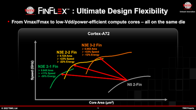
For N3, TSMC's FinFlex technology will allow chip designers to mix and match different kinds of FinFETs within one block to precisely tailor performance, power consumption, and area. For complex structures like CPU cores, such optimizations give a lot of opportunities to increase core performance while still optimizing die sizes. So, we are eager to see how SoC designers will be able to take advantage of FinFlex in the looming N3 era.
FinFlex is not a substitute for node specialization (performance, density, voltages) as process technologies have greater differences than the ibraries or transistor structures within a single process technology, but FinFlex looks to be a good way to optimize performance, power, and costs for TSMC's N3 node. Ultimately, this technology will bring the flexibility of FinFETs a little closer to that of GAAFETs, which are slated to offer adjustable channel widths to get higher performance or reduce power consumption.
Summary
Like TSMC's N7 and N5, N3 will be another family of long-lasting nodes for the world's largest contrast maker of semiconductors. Especially with the jump to GAAFETs coming up at 2nm for TSMC, the 3nm family will be the final family of "classic" leading-edge FinFET nodes from the firm, and one that a lot of customers will stick to for several years (or more). Which, in turn, is why TSMC is prepping multiple versions of N3 tailored for different applications – as well as FinFlex technology to give chip designers some additional flexibility with their designs.
The first N3 chips are set to enter production in the coming months and arrive to the market in early 2023. Meanwhile, TSMC will keep producing semiconductors using its N3 nodes long after it introduces its N2 process technology in 2025.
More...
-
06-16-22, 05:55 PM #11520
Anandtech: TSMC to Expand Capacity for Mature and Specialty Nodes by 50%
TSMC this afternoon has disclosed that it will expand its production capacity for mature and specialized nodes by about 50% by 2025. The plan includes building numerous new fabs in Taiwan, Japan, and China. The move will further intensify competition between TSMC and such contract makers of chips as GlobalFoundries, UMC, and SMIC.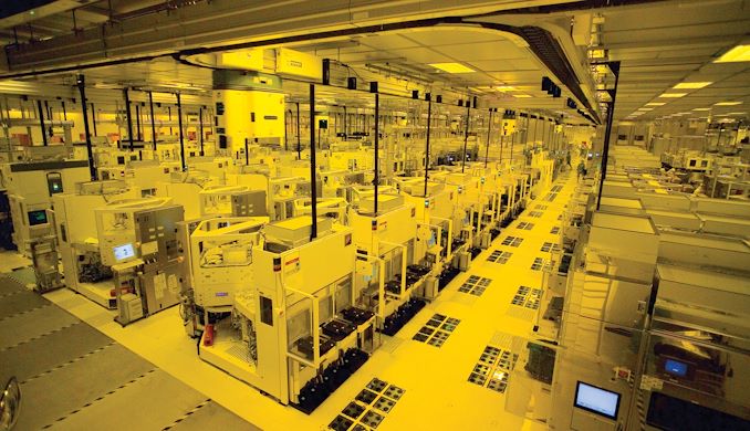
When we talk about silicon lithography here at AnandTech, we mostly cover leading-edge nodes used produce advanced CPUs, GPUs, and mobile SoCs, as these are devices that drive progress forward. But there are hundreds of device types that are made on mature or specialized process technologies that are used alongside those sophisticated processors, or power emerging smart devices that have a significant impact on our daily lives and have gained importance in the recent years. The demand for various computing and smart devices in the recent years has exploded by so much that this has provoked a global chip supply crisis, which in turn has impacted automotive, consumer electronics, PC, and numerous adjacent industries.
Modern smartphones, smart home appliances, and PCs already use dozens of chips and sensors, and the number (and complexity) of these chips is only increasing. These parts use more advanced specialty nodes, which is one of the reason why companies like TSMC will have to expand their production capacities of otherwise "old" nodes to meet growing demand in the coming years.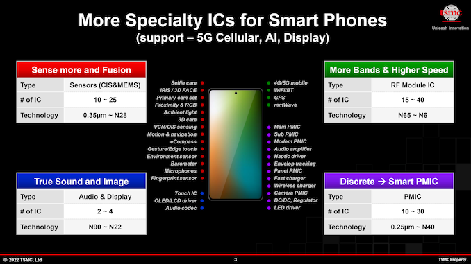
But there is another market that is about to explode: smart cars. Cars already use hundreds of chips, and semiconductor content is growing for vehicles. There are estimates that several years down the road the number of chips per car will be about 1,500 units – and someone will have to make them. Which is why TSMC rivals GlobalFoundries and SMIC have been increasing investments in new capacities in the last couple of years.
TSMC, which has among the largest CapEx budgets in the semiconductor industries (which is challenged only by Samsung) has in recent years been relatively quiet about their mature and specialty node production plans. But at their 2022 TSMC Technology Symposium, the company outlined its plans formally.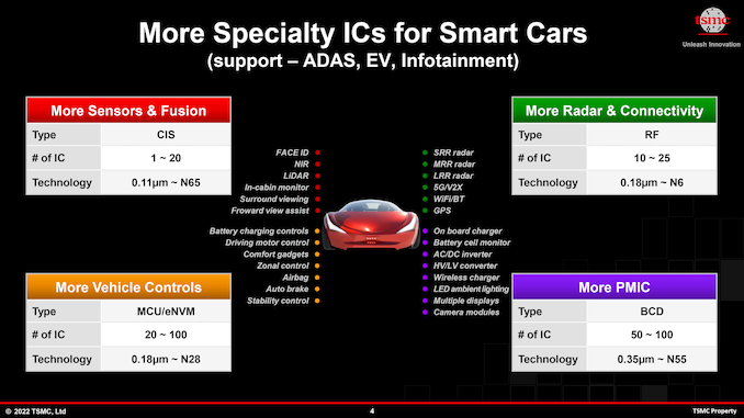
The company is investing in four new facilities for mature and specialty nodes:
- Fab 23 Phase 1 in Kumamoto, Japan. This semiconductor fabrication facility will make chips using TSMC's N12, N16, N22, and N28 nodes and will have a production capacity of up to 45,000 300-mm wafer starts per month.
- Fab 14 Phase 8 in Tainan, Taiwan.
- Fab 22 Phase 2 in Kaohsiung, Taiwan.
- Fab 16 Phase 1B in Nanjing, China. TSMC currently makes chips on its N28 in China, though the new phase was once rumored to be capable of making chips using more advanced nodes.
Increasing mature/specialized capacity by 50% over the next three years is a big shift for the company, and one that will improve TSMC's competitive positions on the market. What is perhaps more important is that the company's specialty nodes are largely based on its common nodes, which allows at least some companies to re-use IP they once developed for compute or RF for a new application.
"[Our] specialty technology is quite unique as it is based on common technology platform [logic technology platform], so our unique strategy is to allow our customer to share or reuse many of the [common] IP," said Kevin Zhang, senior vice president of business development at TSMC. "For example, you have RF capability, you build that RF on a common logic platform, but later you find 'hey someone need a so-called ULV feature to support an IoT product application.' You want to build that on a common platform so you can allow different product lines to be able to share IP across the board, this is very important for our customers so we do want to provide a integrated platform to address the market needs of customer from product perspective.'
There are other advantages too. For example, TSMC's N6RF allows chip designers to combine high-performance logic with RF, which enables them to build products such as modems and other, more unique solutions. Many companies are already familiar with TSMC's N6 logic node, so now they have an opportunity to add RF connectivity to something that benefits from high performance. GlobalFoundries has a similar approach, but since the U.S.-based foundry does not have anything comparable to TSMC's N6, TSMC has an indisputable advantage here.
With its common platform approach for mature nodes as well as specialized technologies, and 50% more capacity, TSMC will be able to offer the world more chips for smart and connected devices in the coming years. Furthermore, it will also benefit TSMC by significantly increasing the company's revenues from mature and specialized nodes, as well as increasing pressure on their rivals.
More...


 Quote
QuoteThread Information
Users Browsing this Thread
There are currently 22 users browsing this thread. (0 members and 22 guests)


Bookmarks