

Results 11,591 to 11,600 of 12091
Thread: Anandtech News
-
10-28-22, 01:00 AM #11591
Anandtech: Intel Reports Q3 2022 Earnings: Back To Profitability, But Still Painful
While always an interesting topic by default, corporate earnings reports in the tech industry have become especially important in the last few months, as the industry prepares to weather what’s expected to be the biggest downturn in demand in the last several years. Intel’s brutal Q2’22 report, which found the company losing money on a GAAP basis for the first time in 5 years, seems to have been a herald of things to come for the largest industry, with AMD and other companies since issuing earnings warnings ahead of their own Q3 reports. So as the first major tech company to publish their complete Q3’22 earnings report, Intel is once again likely to be a barometer of the tech industry’s performance over the past three months.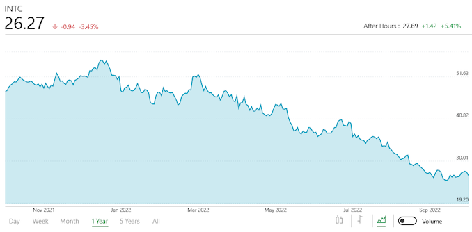
For the third quarter of 2022, Intel reported $15.3B in revenue, a $3.9B decline versus the year-ago quarter. Compared to Intel’s harsh Q2 report, the company has returned to profitability, booking a cool billion dollars in net income, though this is still well below their historical norms. In fact, the company is still operating at a (GAAP) loss, booking an operating income of -$175M. For Q3 at least, it would appear that it’s Intel’s tax situation that’s pushing them into the black, with the company recording a $1.2B tax benefit.
More...
-
10-28-22, 01:00 AM #11592
Anandtech: TSMC Forms 3DFabric Alliance to Accelerate Development of 2.5D & 3D Chiple
Currently the majority of high-end processors are monolithic, but design methodologies are slowly but surely shifting to multi-chiplet modules as leading-edge fabrication technologies get more expensive to use. In the coming years multi-chiplet system-in-packages (SiPs) are expected to become much more widespread, and advanced 2.5D and 3D chip packaging technologies will gain importance. To accelerate and simplify development of 3D designs, TSMC this week established its 3DFabric Alliance.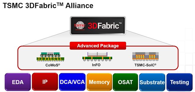
While multi-chiplet SiPs promise to simplify development and verification of highly complex designs, they require brand-new development methodologies as 3D packages bring a number of new challenges. This includes new design flows required for 3D integration, new methods of power delivery, new packaging technologies, and new testing techniques. To make the best use of the benefits of TSMC's 2.5D and 3D packaging technologies (InFO, CoWoS, and SoIC), the chip development industry needs the whole ecosystem to work in concert on chiplet packaging – and this is what 3DFabric Alliance is designed to do.
“3D silicon stacking and advanced packaging technologies open the door to a new era of chip-level and system-level innovation, and also require extensive ecosystem collaboration to help designers navigate the best path through the myriad options and approaches available to them,” said Dr. L.C. Lu, TSMC fellow and vice president of design and technology platform.
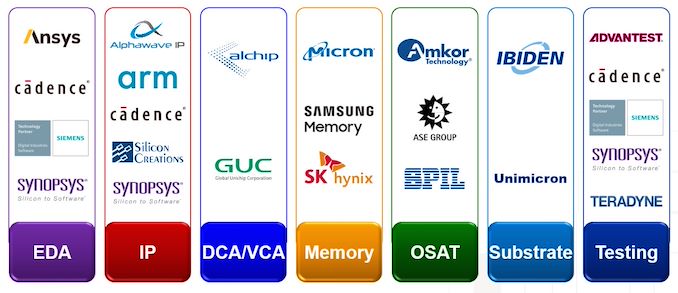
TSMC's 3DFabric Alliance brings together developers of electronic design automation (EDA) tools, intellectual property providers, contract chip designers, memory manufacturers, advanced substrate producers, semiconductor assembly and test companies, and the groups making the equipment used for testing and verification. The alliance currently has 19 members, but over time it is expected to expand as new members join the group.
As the leader of the Alliance, TSMC will set certain ground rules and standards. Meanwhile members of 3DFabric Alliance will co-define and co-develop some of the specifications for TSMC's 3DFabric technologies, will gain early access to TSMC's 3DFabric roadmap and specs to align their plans with the foundry's plans as well as those of other members of the alliance, and will be able to design and optimize solutions that are compatible with the new packaging methods.
Ultimately, TSMC wants to ensure that members of 3DFabric Alliance will offer its clients compatible and interoperable solutions that will enable quick development and verification of multi-chiplet SiPs that use 2.5D and 3D packaging.
For example, to unify the design ecosystem with qualified EDA tools and flows, TSMC has developed its 3Dblox standard. 3Dblox covers various aspects of building multi-chiplet devices featuring 2.5D and 3D packaging methodologies (such as chiplet and interface definitions), including physical implementation, power consumption, heat dissipation, electro-migration IR drop (EMIR), and timing/physical verification.
“Through the collective leadership of TSMC and our ecosystem partners, our 3DFabric Alliance offers customers an easy and flexible way to unlocking the power of 3D IC in their designs, and we can’t wait to see the innovations they can create with our 3DFabric technologies,” added Lu.
Ultimately, TSMC envisions that the alliance will greatly simplify and streamline the process for developing more advanced chips, especially for small and mid-size companies that rely more heavily on outside IP/designs. For example, if a company wants to develop a SiP consisting of logic chiplets stacked together and connected to an HBM3-based memory subsystem, EDA software from Ansys Cadence, Synopsys, and Siemens will allow it to design compatible chiplets, IP providers will sell those blocks the designer does not already have, TSMC will produce silicon, memory producers will offer compatible HBM3 KGSDs (known good stack dies), and then Ase Technology will assemble everything together. Meanwhile companies that do not have their own engineers will be able to order the design of the whole SiP (or individual chiplets) through Alchip or GUC, and then update their product over time if needed without needing to redesign everything, as the SiP will be built in accordance with 3DFabric and 3Dblox standards.
3Dblox is currently supported by four major EDA developers. Eventually it will be supported by all members of the members if the alliance where needed.
While large companies like AMD and Nvidia tend to develop their own IP, interconnection, and packaging technologies, multi-chiplet SiPs promise to make the development of complex, chiplet-style processors accessible to smaller companies. For them, standard third-party IP, fast time-to-market, and proper integration are key to success, so 3DFabric Alliance and what it brings will be vital for them.
Source: TSMC
More...
-
10-28-22, 11:40 AM #11593
Anandtech: The CyberPower ValuePro VP1600ELCD 1600 VA UPS Review: A Solid Budget Powe
In today's review, we are taking a look at the ValuePro VP1600ELCD, a popular low-cost UPS from CyberPower, the renowned US-based power systems manufacturer. As the name suggests, it is a product developed with value in mind, in an effort to entice home users and small business owners. Truly, features such as built-in AVR and completely silent operation are very enticing at this price range from a renowned brand name. As with all things that are too good to be true though, there are tradeoffs.
More...
-
11-03-22, 09:50 PM #11594
Anandtech: AMD Reveals Radeon RX 7900 XTX and 7900 XT: First RDNA 3 Parts To Hit Shel
With AMD’s first-wave of Zen 4 CPUs now in the books with the Ryzen 7000 series, the consumer arm of AMD is now shifting its attention over to its graphics business. In a presentation that ended moments ago dubbed “together we advance_gaming”, Dr. Lisa Su and other AMD leaders laid out the future of AMD’s graphics products. And that future is the RDNA 3 architecture, which will be the basis of the new Radeon RX 7900 XTX and Radeon RX 7900 XT video cards.
The two cards, set to be released on December 13th, will be the first products released using the RDNA 3 architecture. According to AMD, the new flagship 7900 XTX will deliver up to 70% more performance at 4K than their previous flagship, the 6950 XT. This performance boost comes curtesy of several architectural improvements in RDNA that cumulatively offer 54% higher performance per watt than RDNA 2, as well as higher clockspeeds courtesy of TSMC’s 5nm (and 6nm) processes, and higher overall power consumption.
The full-fledged RX 7900 XTX will be hitting the streets at $999. Meanwhile the second-tier RX 7900 XT will run for $899.
More...
-
11-03-22, 09:50 PM #11595
Anandtech: AMD RDNA 3 GPU Unveil "together we advance_gaming Live Blog (1pm PT/20:00
Following hot on the heels of AMD’s major CPU launch of the year – the Zen 4 architecture and Ryzen 7000 family – today AMD will be giving their GPU architecture its moment in the sun with their gaming-centric “together we advance_gaming” event. Today’s event will be all about AMD’s next-generation Radeon GPU architecture, RDNA 3, which among other things, promises a 50% improvement in performance-per-watt over the previous-generation RDNA 2 (Radeon RX 6000 series) parts.
Notably, unlike AMD’s CPU event back in August, AMD has held their (video) cards closer to their proverbial chest for this event. We know that it’s all about the RDNA 3 architecture, but AMD is being quieter about product information and details. For example, any “Radeon RX 7000 series” branding is completely absent from all of AMD’s official communiques. So while the Radeon RX 7000 series is still the branding we’re expecting to see, AMD is leaving themselves a noticeable amount of room to throw some curveballs here.
In any case, AMD has offered a few high-level details on the RDNA 3 architecture throughout the year. The biggest items disclosed thus far are that AMD is targeting another 50% increase in performance-per-watt, and that these new GPUs (Navi 3x) will be made on a 5nm process (undoubtedly TSMC’s). Past that, AMD hasn’t given any guidance on what to expect for performance.
One interesting aspect, however, is that AMD has confirmed that they will be employing chiplets with this generation of products. To what extent, and whether that’s on all parts or just some, remains to be seen. But chiplets are in some respects the holy grail of GPU construction, because they give GPU designers options for scaling up GPUs past today’s die size (reticle) and yield limits. That said, it’s also a holy grail because the immense amount of data that must be passed between different parts of a GPU (on the order of terabytes per second) is very hard to do – and very necessary to do if you want a multi-chip GPU to be able to present itself as a single device.
We’re also apparently in store for some more significant upgrades to AMD’s overall GPU architecture. Though what exactly a “rearchitected compute unit” and “optimized graphics pipeline” fully entail remains to be seen.
The answers to all that, and more, are coming up here in a few hours. So be sure to join us today, November 3rd, at 1pm Pacific (20:00 UTC) for our full live blog coverage of AMD’s latest GPU announcements. We can’t wait!
More...
-
11-08-22, 08:30 AM #11596
Anandtech: Intel Launches Raptor Canyon: Desktop Raptor Lake Sizzles in NUC13 Extreme
Intel is officially taking the wraps off the first member of their Raptor Lake-based NUC13 family today. The NUC13 Extreme (like the three previous Extreme NUCs) caters to the gamers and content creators requiring leading edge performance and high-end discrete GPU support. Unlike the mainstream NUCs which have been consistently maintaining an ultra-compact form-factor profile, the Extreme family has slowly grown in size to accommodate flagship CPUs and discrete GPUs. These systems integrate a motherboard in a PCIe add-in card form factor (the Compute Element) and a baseboard that provides additional functionality with PCIe slots and other I/O features. As a refresher, Intel created the NUC Extreme category with the introduction of the Ghost Canyon NUC family in 2019. This was followed by the Tiger Lake-based Beast Canyon NUC in 2021 and the Alder Lake-based Dragon Canyon NUC earlier this year. The latest member of this family is today's introduction - the Raptor Canyon NUC based on the Shrike Bay Compute Element.
The NUC Extreme family has grown in physical footprint with each generation, and the NUC13 Extreme is Intel's biggest one yet. Coming in at 317mm x 129mm x 337mm (13.7L), this is more of a traditional tower desktop than the NUCs that the market has grown accustomed to. However, this size has allowed Intel to integrate flagship components. The Shrike Bay Compute Element supports socketed LGA 1700 processors with a PL1 of 150W and PL2 of 250W (tau of 28s). The vertical centering of the baseboard within the case enables plenty of isolation between the Compute Element on the top and the discrete GPU on the bottom. Triple-slot dGPUs up to 12.5" in length are supported.
The NUC13 Extreme Kit comes in three flavors, while the Shrike Bay Compute Element itself has six variations. These allow system integrators and OEMs to offer a wide variety of systems targeting different market segments. The table below summarizes the key differences between the three NUC13 Extreme kits.
Each kit SKU corresponds to a NUC13SBB Shrike Bay Compute Element. In addition, Intel is also readying the NUC13SBBi(9/7/5)F variants that come with the KF processors - those Compute Elements do not have any Thunderbolt 4 ports. The HDMI port / graphics outputs are also not present. The three KF SKUs also forsake the 10GbE port.Intel NUC13 Extreme Kits (Raptor Canyon) Model NUC13RNGi9 NUC13RNGi7 NUC13RNGi5 CPU Intel Core i9-13900K
Raptor Lake, 8P + 16E / 32T
5.8 GHz (Turbo) / 5.4 GHz (P) / 4.3 GHz (E)
125W TDP (Up to 253W)Intel Core i7-13700K
Raptor Lake, 8P + 8E / 24T
5.4 GHz (Turbo) / 5.3 GHz (P) / 4.2 GHz (E)
125W TDP (Up to 253W)Intel Core i5-13600K
Raptor Lake, 6P + 8E / 20T
5.1 GHz (Turbo) / 5.1 GHz (P) / 3.9 GHz (E)
125W TDP (Up to 181W)GPU Intel UHD Graphics 770 (300 MHz - 1.65 GHz) Intel UHD Graphics 770 (300 MHz - 1.60 GHz) Intel UHD Graphics 770 (300 MHz - 1.50 GHz) Memory 2x DDR5-5600 SODIMMs
(up to 64GB)Motherboard (Compute Element) 295.3mm x 136.5mm x 46.1mm (Custom) Storage 1x CPU-attached PCIe 4.0 x4 M.2 2280
1x PCH-attached PCIe 4.0 x4 M.2 2242 / 2280
1x PCH-attached PCIe 4.0 x4 / SATA M.2 2242 / 2280
2x SATA 6 Gbps (on baseboard)I/O Ports 2x USB4 / Thunderbolt 4 (Type-C) (Rear)
6x USB 3.2 Gen 2 Type-A (Rear)
1x USB 3.2 Gen 2 Type-C (Front)
2x USB 3.2 Gen 1 Type-A (Front)Networking Intel Killer Wi-Fi 6E AX1690i
(2x2 802.11ax Wi-Fi inc. 6 GHz + Bluetooth 5.2 module)
1× 2.5 GbE port (Intel I226-V)
1x 10 GbE port (Marvell AQtion AQC113C)Display Outputs 2x DP 2.0 (1.4 certified) (via Thunderbolt 4 Type-C, iGPU)
1x HDMI 2.1 (up to 4Kp60) (rear, iGPU)Audio / Codec 7.1 digital (over HDMI and Thunderbolt 4)
Realtek ALC1220 Analog Audio / Microphone / Speaker / Line-In 3.5mm (Rear)
USB Audio 3.5mm combo audio jack (Front)Enclosure Metal
Kensington lock with base securityPower Supply FSP750-27SCB 750W Internal PSU Dimensions 337mm x 317mm x 129mm / 13.7L Chassis Expansion One PCIe 5.0 x16 with triple-slot GPU support up to 317.5mm in length Customizable RGB LED illumination on chassis underside
CEC support for HDMI port
Power LED ring in front panel
3-year warranty
The block diagram below gives some insights into the design of the system in relation to the I/O capabilities. Note that the system continues to use the Z690 chipset that was seen in the Dragon Canyon NUC.
PCIe x16 bifurcation (x8 + x8) is possible for the Gen 5 lanes. However, the baseboard design in the Raptor Canyon NUC kits does not support it. This is yet another aspect that OEMs could use to differentiate their Shrike Bay-based systems from the NUC13 Extreme.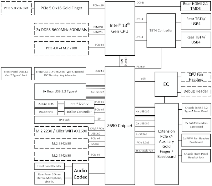
Intel has provided us with a pre-production engineering sample of the flagship Raptor Canyon NUC (augmented with an ASUS TUF Gaming RTX 3080Ti GPU) for review, and it is currently being put through the paces. The 150W PL1 and microarchitectural advances in Raptor Lake have ensured that the benchmark scores are off the charts compared to the previous NUC Extreme models, albeit at the cost of significantly higher power consumption. On the industrial design side, I have been very impressed. By eschewing a fancy chassis and opting for a simple cuboid, Intel has ensured that all the I/O ports are easily accessible, installation of components is fairly straightforward, and cable management is hugely simplified. The increased dimensions of the chassis are well worth these advantages over the previous NUC Extreme models. Stay tuned for a comprehensive review later this week.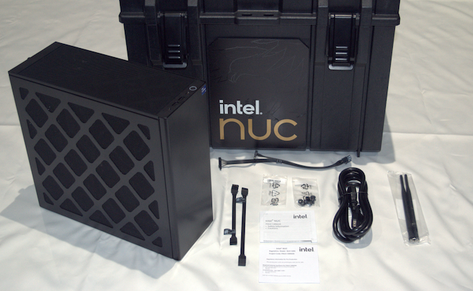
More...
-
11-18-22, 09:48 AM #11597
Anandtech: WD_BLACK P40 Game Drive USB 3.2 Gen 2x2 Portable SSD Review: Balanced Stor
Western Digital had announced new products in the WD_BLACK lineup back in May 2022 to augment their offerings in the gaming market. The WD_BLACK P40 Game Drive SSD was part of the set, and became widely available last quarter. Western Digital has positioned the portable drive (PSSD) as a mid-range alternative to the premium WD_BLACK P50 Game Drive SSD. Sporting a USB 3.2 Gen 2x2 (20 Gbps) interface, the drive launched at a much lower price point compared to the P50 despite the addition of RGB lighting to the case. What corners has Western Digital cut in this mid-range offering, and what do gamers have to lose in going with the P40 over competing PSSDs? This review provides some answers.
More...
-
11-21-22, 08:41 PM #11598
Anandtech: Sponsoed Post: Trying to Pick Out Your New RTX 40 Series GPU? ASUS Has Two
ASUS is introducing two versions of the GeForce RTX 4090 and 4080 in its Republic of Gamers and TUF Gaming lines, giving gamers stylish and robust options for the latest graphics cards.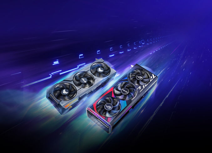
More...
-
12-02-22, 02:22 AM #11599
Anandtech: Site News: December 1st Outage
As many of you noticed, AnandTech has spent several hours offline today. We are still in recovery mode at the moment (as I write this, the site has been restored to a copy from November 25th), but now that our major restoration efforts are completed, I wanted to offer you guys a brief update on the status of AnandTech.
At around 13:00 UTC (5am PT) today, the on-site cloud storage for AnandTech’s hosting provider became corrupted. As a result, AnandTech (and some other sites) were brought offline. Due to the nature of the corruption and the need to begin restoration efforts ASAP, we opted to restore the site from an off-site cold storage backup, rather than trusting the questionable on-site storage.
This is the first time we’ve ever had to execute our off-site data recovery plan before. And while it meant AT took a bit longer to restore than would be ideal, ultimately everything worked out and proved the necessity for off-site backups.
We’re still working to restore content from the last few days. Articles will be back, but we’ve likely lost any comments and user account registrations/updates made since midday Friday. Sorry about that! And thank you for bearing with us during today's outage.
More...
-
12-08-22, 05:20 AM #11600
Anandtech: TSMC Unveils Major U.S. Fab Expansion Plans: 3nm and $40 Billion by 2026
TSMC this week held its Arizona fab 'first tool-in' ceremony, where alongside celebrating its first US fab, the company also announced major expansion plans for the production facility. The world's largest foundry is set to invest tens of billions of dollars in the next phase of its Fab 21 near Phoenix, Arizona, to significantly expand its capacity and start production of chips on its N3 process technologies there by 2026.
Construction of TSMC's Fab 21 phase 1 in Arizona was completed earlier this year, and this week the company began installation of production tools into the facility. The fab will be equipped with tools from companies like ASML, Applied Materials, KLA, Lam Research, and Tokyo Electroni in the next few quarters, and it is scheduled to come online in early 2024. The fab will be producing chips using various process technologies that belong to TSMC's N5 family, which now includes N5, N5P, N4, N4P, and N4X nodes. Production capacity of this phase of the fab will be around 30,000 wafer starts per month (WSPM), though the precise number will depend on actual technologies and designs.
Companies like AMD, Apple, and NVIDIA are set to run orders through Fab 21 phase 1 to produce their advanced chips in the U.S. for the first time in years.
But that isn't all that TSMC has in store for Fab 21. The company has announced that they now intend to build a second fab on the site, further expanding their US production capacity and setting up an even newer production line.
The new Arizona fab will expand TSMC's capacity at the site to around 50,000 WSPM and will bring TSMC's total investments in the site to $40 billion. Notably, that's a $28B jump over the initial $12B investment TSMC made in their first Arizona fab, underscoring how costs continue to rise for newer fabs, but also that TSMC is becoming more comfortable with making larger infrastructure investments within the US. TSMC expects annual revenue from Arizona fabs to be in $10 billion per year ballpark, according to a Reuters report. Meanwhile, TSMC's clients using the fabs will generate about $40 billion in revenue selling products made by the foundry in the U.S.
Set to come online in 2026, the second Arizona fab will be starting life a generation ahead of its initial counterpart, producing chips on TSMC's N3 family of production nodes, which includes N3, N3E, N3P, N3S, and N3X. TSMC is expected to deliver its first N3 chips to a client in early 2023, so while the fab still represents cutting-edge technology as of the time of its inception, by the time it comes online it will technically be a trailing-edge fab. TSMC has previously indicated that they would be keeping leading-edge production within Taiwan – in large part because that's where their actual R&D takes place – so the company's updated Arizona fab plans are consistent with that stance.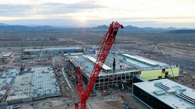
With regards to capacity, the new Arizona fab, like its existing sibling, will be another "MegaFab" in TSMC parlance. That is to say a mid-range fab producing around 25,000 wafer starts per month. TSMC hasn't disclosed a specific output figure for just the new fab, but with Fab 21 slated to offer 20,000 WSPM, it looks like this fab will be a bit bigger, at closer to 30,000 WSPM. Still, with a combined capacity of 50,000 wafers per month, TSMC's Arizona facility is still among one of TSMC's smaller operations – 50,000 wafers is only half the production capacity a single one of TSMC's class-leading GigaFabs. So even with a second fab line, TSMC's US operations will only represent a relatively small fraction of the company's overall chip fab capacity.
Looking forward, TSMC has already begun construction of the second Arizona fab, and given the usual fab construction timelines, we can expect the shell to be complete by early 2024. After which it will take TSMC around another two years to equip it.
Gallery: TSMC Supplier Tool Photos PVD Endura II_thumb.jpg)
 XP8 QCM_thumb.png)
 YieldStar 385H_thumb.png)
 SpectraFilm F1_thumb.png)
 Argos MACH IV_thumb.png)
 CELLESTA-i_thumb.png)
Meanwhile, TSMC is set to start producing chips using its N2 node in Taiwan in the second half of 2025. That node will use will be TSMC's first node to use their nanosheet-based gate-all-around field-effect transistors (GAAFETs), and over time will gain backside power delivery. Still, since not all products need a leading-edge node, TSMC won't have any trouble lining up customers for their N3 US domestic capacity.
"A strong, geographically diverse, and resilient supply chain is essential to the global semiconductor industry," said Lisa Su, chief executive and chairman of AMD. "TSMC's investment and expansion in Arizona is extremely important and mission critical for both the semiconductor industry and our extended ecosystem of partners and customers. AMD expects to be a significant user of the TSMC Arizona fabs and we look forward to building our highest performance chips in the United States."
Source: TSMC
More...


 Quote
QuoteThread Information
Users Browsing this Thread
There are currently 17 users browsing this thread. (0 members and 17 guests)


Bookmarks