

Results 11,671 to 11,680 of 12094
Thread: Anandtech News
-
03-27-23, 11:27 AM #11671
Anandtech: Intel NUC 13 Pro Arena Canyon Review: Raptor Lake Brings Incremental Gains
Ultra-compact form-factor PCs have emerged as bright spots in the PC market over the last decade after Intel introduced the NUC. The company celebrated the 10-year anniversary of its introduction last year with the Alder Lake-based 4"x4" Wall Street Canyon NUCs. Barely a couple of quarters down the road, Intel is updating its Pro line of UCFF NUCs with the 13th Gen. Core Processors (Raptor Lake). The new Arena Canyon NUCs carry forward the same hardware features of the Wall Street Canyon SKUs, with the only update being the change in the internal SoC.
Raptor Lake-P brings incremental gains in terms of both performance and power efficiency over Alder Lake-P. We already saw one of Intel's partners - ASRock Industrial - take the lead in delivering UCFF mini-PCs based on Raptor Lake-P. How does Intel's own efforts in the segment pan out? Read on to find out more about Intel's lineup of Arena Canyon NUCs and a detailed investigation into the performance profile of the NUC13ANKi7 based on the Core i7-1360P.
More...
-
03-28-23, 02:38 AM #11672
Anandtech: MinisForum Launches NAB6 mini-PC With Dual 2.5G Ethernet Ports
MinisForum is a well-known manufacturer from Shenzhen, China, specializing in compact systems. The company recently added the NAB6 to its diverse portfolio of mini-PCs powered by Intel processors. The NAB6, which leverages Intel's Core i7-12650H (Alder Lake) processor, offers not one but two high-speed 2.5G Ethernet ports. The feature is common on higher-end motherboards but rarely on a mini-PC.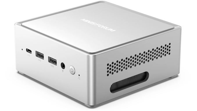
The NAB6 is a compact system that will leave a small footprint on even the most miniature desks. It arrives with a minimalistic but slick exterior. MinisForum doesn't list the dimensions or the materials used in the device's fabrication on the product page. Instead, the manufacturer highlights the device's focus on maintenance and upgradability. Getting inside the NAB6 is easy and fast. A single press on the top plate is sufficient to pop it off for upgrading or switching out memory or SSDs. The NAB6 has an adequate cooling solution that consists of two copper heat pipes that transfer the heat from the processor to the compact heatsink, where a small cooling fan dissipates the heat through two air outlets. As modest as the cooler may look, it suffices to keep the 45 W Intel 12th Generation Alder Lake-H processor cool.
Only one processor option is available to consumers on the NAB6: the last-generation Core i7-12650H. The 10-core hybrid mobile chip wields six P-cores, four E-cores, and 24 MB of L3 cache. The Core i7-12650H has a 4.7 GHz boost clock but operates within 45 W PBP and 115 W MTP limits. Consumers can pair the 10nm chip with up to 64 GB of DDR4-3200 memory, as there are two SO-DIMM memory slots inside the NAB6. The mini-PC has a single M.2 slot that adheres to the PCIe 4.0 interface. It supports M.2 drives with a length of 80 mm and up to 2 TB of storage. If buyers purchase the NAB6 with an SSD from MinisForum, the company includes an active heatsink with the drive. Alternatively, consumers can use the heatsink included with their SSDs or one of the numerous third-party heatsinks on the market. The NAB6's design has a specially placed vent where the SSD is located to allow M.2 SSD heatsinks with active cooling to expel the heat outside the device freely. The NAB6 also provides spacing for a standard 2.5-inch SATA SSD or hard drive for secondary storage.
One of the NAB6's strong suits is the presence of two 2.5G Ethernet ports, making the mini-PC a terrific asset in home and enterprise environments with a high-bandwidth Internet connection. Unfortunately, MinisForum didn't specify the model of the two 2.5G Ethernet controllers. There's a small compromise, though. The NAB6 doesn't have wireless connectivity by default, so consumers must spend extra to get that wireless connection. Instead, the motherboard has reserved a regular M.2 2230 slot for a WiFi module.MinisForum NAB6 Specifications CPU Intel Core i7-12650H GPU UHD Graphics (64 EUs, 1.4 GHz) Memory 2 x DDR4 SO-DIMM slots (Up to 64 GB of DDR4-3200) Storage M.2 PCIe 4.0 M.2 2280 (Up to 2TB) DFF 1 x 2.5" SSD/HDD Wireless N/A Ethernet 2 x 2.5 Gigabit Ethernet with RJ45 Display Outputs 2 x HDMI 2.1 Audio 2 x 3.5 mm combo jack USB 1 x USB 3.2 Gen 1 Type-C
1 x USB 3.2 Type-C (DisplayPort)
1 x USB 3.2 Type-C (Alt DP, Data Transfer)
4 x USB 3.2 Gen 2 Type-AThunderbolt 4 N/A PSU External OS Barebones Model (No OS)
Windows 11 Home pre-installedPricing Barebones: $459
16 GB + 512 GB SSD: $559
32 GB + 512 SSD: $609
32 GB + 1 TB SSD: $659
MinisForum didn't cheap out on connectivity on the NAB6. The device's front panel conveniently provides one USB 3.2 Gen 2 Type-C port and two USB 3.2 Gen 2 Type-A ports. If that's not enough, the rear panel houses two more USB 3.2 Gen 2 Type-A ports and two USB 3.2 Type-C ports (one's DP only, and the other supports Alt DP and data transfer). There are also two standard HDMI 2.1 ports. As a result, the NAB6 is an excellent option for heavy multitaskers since the mini-PC can handle up to four simultaneous displays at 4K with a 60 Hz refresh rate.
The barebone NAB6 system sells for $459. The 16 GB memory and 512 GB SSD configuration retails for $559, whereas the 32 GB variant with the same SSD costs $609. The highest-specced variant, which sports 32 GB of memory and a 1 TB SSD, carries a $659 price tag. MinisForum is presently running a limited-time discount on its website for the NAB6, where consumers can save up to 22% if they put in their orders now. Unfortunately, the vendor didn't specify the period for the promotion. Buyers will also have to factor in the shipping cost. MinisForum has a store on Amazon, so there's free shipping for Amazon Prime members. However, the company hasn't listed the NAB6 on Amazon yet. MinisForum plans to ship NAB6 orders in mid-April.
More...
-
03-28-23, 02:38 AM #11673
Anandtech: NVIDIA's cuLitho to Speed Up Computational Lithography for 2nm and Beyond
Production of chips using leading-edge process technologies requires more compute power than ever. To address requirements of 2nm nodes and beyond, NVIDIA is rolling out its cuLitho software library that uses the company's DGX H100 systems based on H100 GPUs and promises to increase performance available to mask shops within a reasonable amount of consumed power by 40 times.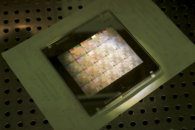
Modern process technologies push wafer fab equipment to its limits and often require finer resolution than is physically possible, which is where computational lithography comes into play. The primary purpose of computational lithography is to enhance the achievable resolution in photolithography processes without modifying the tools. To do so, CL employs algorithms that simulate the production process, incorporating crucial data from ASML's equipment and shuttle (test) wafers. These simulations aid in refining the pellicle (photomask) by deliberately altering the patterns to counteract the physical and chemical influences that arise throughout the lithography and patterning steps.
There are several computational lithography techniques, including Resolution Enhancement Technology (RET), Inverse Lithography Technology (ILT, a method to reduce manufacturing variations by utilizing non-rectangular shapes on the photomask), Optical Proximity Correction (OPC, a technique for improving photolithography by correcting image inaccuracies resulting from diffraction or process-related impacts), and Source Mask Optimization (SMO). All of them are widely used at today's fabs.
Meanwhile, compute-expensive techniques like inverse lithography technology and source mask optimization are specific to a given design. They have to be implemented individually for each chip to ensure appropriate resolution and avoid yield-limiting hotspots. Synthesis of pellicles that use RET, ILT, OPC, and SMO involves the usage of computational lithography. As nodes get thinner, the complexity of computations increases, and compute horsepower becomes a bottleneck for mask shops as each modern chip uses dozens of pellicles. For example, NVIDIA's H100 uses 89 of them.
NVIDIA says that computational lithography currently consumes tens of billions of CPU hours every year and, therefore, enormous power. Meanwhile, highly parallel GPUs like NVIDIA's H100 promise higher performance at lower cost and power consumption. In particular, NVIDIA says that 500 of its DGX H100 systems packing 4000 of its H100 GPUs (that consume 5 MW of power) and using computational lithography software that uses cuLitho can offer the performance of 40,000 CPU-based systems which consume 35 MW that TSMC uses today. The company also goes on to say that mask makers can produce 3 – 5 times more pellicles per day using nine times less power than they use today once they start relying on GPU-accelerated computational lithography, another claim that requires verification by actual mask shops, but which gives a basic understanding where the company wants to go.
"With lithography at the limits of physics, NVIDIA's introduction of cuLitho and collaboration with our partners TSMC, ASML, and Synopsys allows fabs to increase throughput, reduce their carbon footprint and set the foundation for 2nm and beyond."
While performance targets set by NVIDIA are impressive, it should be noted that the cuLitho software library for computational lithography must be incorporated in software offered by ASML, Synopsys, and TSMC well used by their partners, among mask shops. For current-generation lithography (think 7 nm, 5 nm, and 3 nm-class nodes), mask shops already use CPU-based computational lithography solutions and will continue to do so for at least a while. This is perhaps why NVIDIA is discussing its computational lithography efforts in context with next-generation 2 nm-class nodes and beyond. Meanwhile, it makes sense to expect foundries and mask shops to at least try deploying NVIDIA's cuLitho for some of their upcoming 3 nm-class nodes to increase yields and performance. TSMC, for example, will start to qualify cuLitho in mid-2023, so expect the platform to be available to the company's customers beginning in 2024.
"Computational lithography, specifically optical proximity correction, or OPC, is pushing the boundaries of compute workloads for the most advanced chips," said Aart de Geus, chief executive of Synopsys. "By collaborating with our partner NVIDIA to run Synopsys OPC software on the cuLitho platform, we massively accelerated the performance from weeks to days! The team-up of our two leading companies continues to force amazing advances in the industry."
An official statement by NVIDIA states that "A fab process change often requires an OPC revision, creating bottlenecks." "cuLitho not only helps remove these bottlenecks, but it also makes possible novel solutions and innovative techniques like curvilinear masks, high NA EUV lithography, and sub-atomic photoresist modeling needed for new technology nodes."
Extra compute horsepower available for computational lithography applications will come in particularly handy for the next generation of production nodes that will use High-NA lithography scanners and will mandate the usage of ILT, OPC, and SMO to consider physical peculiarities of lithography scanners and resists to ensure decent yields, low variation (i.e., foreseeable performance and power consumption), and predictable costs. Meanwhile, computational costs for RET, ILT, OPC, and SMO will inevitably increase at 2 nm and beyond, so it looks like NVIDIA will introduce its cuLitho platform at a good time.
More...
-
03-29-23, 01:07 AM #11674
Anandtech: Kingston Launches Fury Beast And Fury Renegade DDR5 Memory in White
Kingston Fury, the gaming and high-performance division of Kingston Technology Company, Inc., has expanded the aesthetics of the company's Fury DDR5 memory portfolio. The Fury Beast and Fury Renegade DDR5 memory lineups now arrive with a white heat spreader design. As a result, consumers of both AMD and Intel platforms can take advantage of the new memory kits when putting together a PC with a white theme.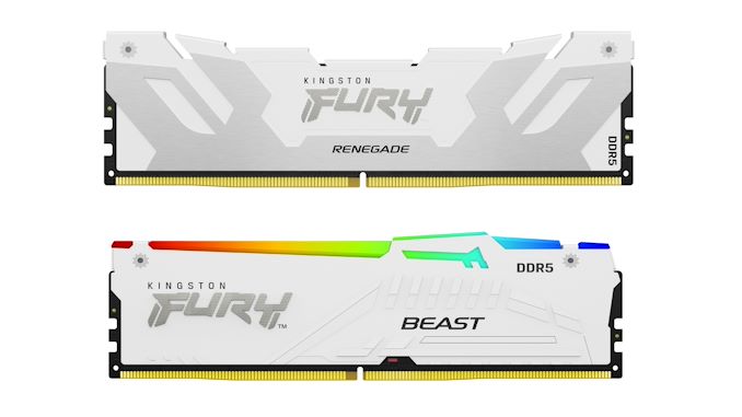
The Fury Beast and Fury Renegade memory kits arrive in vanilla and RGB variants. In the case of the Fury Beast, the non-RGB version measures 34.9 mm, whereas the RGB version stands at 42.23 mm. The memory sticks to a single color, either black or white. On the other hand, the Fury Renegade is slightly taller at 39.2 mm. The RGB-illuminated trim is 44 mm in height. Unlike the Fury Beast, the Fury Renegade rocks a dual-tone exterior in either black and silver or the more recent white and silver combination.
Included within the RGB variations of the Fury Beast and Fury Renegade is Kingston's patented Infrared Sync technology, which, as the name implies, keeps the illumination on the memory module in sync. Kingston provides the company's proprietary Fury CTRL software for users to control the lighting, or they can use the included RGB software from their memory vendors.
Kingston commercializes the Fury Beast and Fury Renegade as individual memory modules and dual-DIMM memory kits. Unfortunately, consumers that want a quad-DIMM memory kit are out of luck until next month. Kingston still uses standard 16 gigabit dies with the brand's DDR5 memory kits. As a result, the company cannot match other vendors who have hit 192 GB (4 x 48 GB) capacity with non-binary memory modules.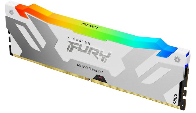
Kingston Fury Renegade DDR5 memory with white heatsink
The Fury Beast portfolio caters to mainstream consumers and offers more varieties. The speeds span from 4,800 MT/s to 6,000 MT/s, with memory kit capacities starting at 16 GB. There are Intel XMP 3.0- and AMD EXPO memory kits. The DDR5-4800 memory kit has CL 38-38-38 timings and is plug-and-play friendly. The higher-grade memory kits come with either Intel XMP 3.0 or AMD EXPO support. The Intel version of the Fury Beast DDR5-6000 memory kit sports 40-40-40 timings and requires 1.35 volts. On the contrary, the AMD version possesses better memory timings (CL 36-38-38) while using the same voltage.Fury Beast Specifications Frequency Latency Timings Capacities DDR5-6000 40-40-40 (1.35 V)
36-38-38 (1.35 V)8 GB (1 x 8 GB)
16 GB (1 x 16 GB)
16 GB (2 x 8 GB)
32 GB (2 x 16 GB)
64 GB (2 x 32 GB)DDR5-5600 40-40-40 (1.25 V)
36-38-38 (1.25 V)8 GB (1 x 8 GB)
16 GB (1 x 16 GB)
16 GB (2 x 8 GB)
32 GB (2 x 16 GB)
64 GB (2 x 32 GB)DDR5-5200 40-40-40 (1.25 V)
36-40-40 (1.25 V)8 GB (1 x 8 GB)
16 GB (1 x 16 GB)
16 GB (2 x 8 GB)
32 GB (2 x 16 GB)
64 GB (2 x 32 GB)DDR5-4800 38-38-38 (1.10 V) 8 GB (1 x 8 GB)
16 GB (1 x 16 GB)
16 GB (2 x 8 GB)
32 GB (2 x 16 GB)
64 GB (2 x 32 GB)
The Fury Renegade series targets gamers and enthusiasts. The memory kits start where the Fury Beast left off. The slowest Fury Renegade memory kit clock in at 6,000 MT/s, and the fastest option maxes out at 7,200 MT/s. Kingston only sells the Fury Renegade in 32 GB and 64 GB kit capacities. All Fury Renegade memory kits are Intel XMP 3.0-certified. The DDR5-7200 memory kit, available only in 32 GB (2 x 16 GB), has the memory timings configured to CL 38-44-44 and pulls 1.45 volts.Fury Renegade Specifications Frequency Latency Timings Capacities DDR5-7200 38-44-44 (1.45 V) 16 GB (1 x 16 GB)
32 GB (2 x 16 GB)DDR5-6800 36-42-42 (1.40 V) 16 GB (1 x 16 GB)
32 GB (2 x 16 GB)DDR5-6400 32-39-39 (1.40 V) 16 GB (1 x 16 GB)
32 GB (2 x 16 GB)DDR5-6000 32-38-38 (1.35 V) 16 GB (1 x 16 GB)
32 GB (2 x 16 GB)
32 GB (1 x 32 GB)
64 GB (2 x 32 GB)
In addition, Kingston backs its Fury Beast and Fury Renegade products with a limited lifetime warranty. The Fury Beast memory kits start at $69, $119, and $228 for the 16 GB, 32 GB, and 64 GB options, respectively. Meanwhile, the starting prices for the Fury Renegade 32 GB and 64 GB memory kits are $159 and $368, respectively.
More...
-
03-29-23, 01:07 AM #11675
Anandtech: JOLED Files for Bankruptcy: Set to Transfer OLED IP to JDI and Close Down
JOLED, a Japan-based producer of OLED panels and displays, said it had applied for bankruptcy protection at the Tokyo District Court, citing total liabilities of ¥33.7 billion ($257 million). It also supplied OLED displays for Apple's smartwatches. The company will transfer its patents and R&D operations to Japan Display Inc and will shut down its manufacturing, affecting makers of high-end OLED-based displays and TVs, including Asus, Eizo, LG, and Sony.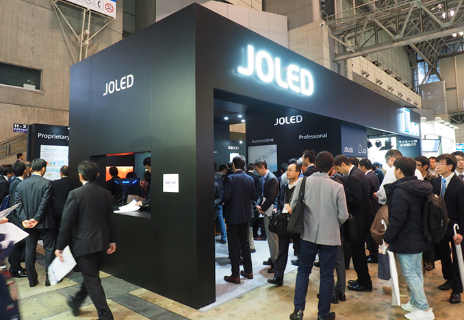
The Innovation Network Corporation of Japan (INCJ), the main shareholder of JOLED, said it could not expect other stakeholders to help bail the company out, reports Nikkei. As a result, JOLED will shut down two plants located in Japan and terminate approximately 280 workers as it exits the OLED panel manufacturing and sales. Additionally, JOLED has reached an agreement to transfer its technology and development operations, which employ roughly 100 people, to Japan Display Inc., which is also co-owned by INCJ.
"We could not expect relevant parties to make additional investments," said Mikihide Katsumata, the president of INCJ.
Established in 2015, JOLED bet on its high-speed inkjet printing technology for EL layer formation as it promised to increase productivity and lower production costs of OLED panels, which was projected to be its key advantage over rivals. But it took the company years to begin mass production of its OLED panels using its innovative method. The company's OLED panels production facility in Nomi started operation in 2019, and it began making OLED display modules at its site in Chiba in 2020. Essentially, the company only began to produce its OLED products in high volumes in 2021.
By that time, such companies dominated the market of OLED panels, including BOE Display, China Star Optoelectronics Technology (CSOT), LG Display, and Samsung Display, so it has not been easy for JOLED to establish its presence in the market. But JOLED has still managed to ink deals to supply high-end OLED panels to Asus and Eizo, which used them for professional and premium products, and Apple, which used its screens for Apple Watch. Also, JOLED sold its panels to Sony and LG and marketed them under its own OLEDIO brand.
Unfortunately for the company, it has been bleeding money on its operations and was never profitable. Its owners decided to pull the plug on JOLED, close its manufacturing facilities, and transfer its engineers and IP to JDI, which considers OLED technologies particularly important.
JOLED's Nomi site in Ishikawa, Japan
JDI has agreed to acquire JOLED's OLED IP, know-how, and engineers, as part of its growth strategy. The agreement focuses on keeping OLED technology development by incorporating JOLED's expertise into JDI's operations and providing employment opportunities for JOLED engineering teams. Meanwhile, JDI will not be taking over JOLED's unprofitable product manufacturing and sales divisions, which JOLED has chosen to divest. Yet, JDI has committed to facilitating the smooth termination and liquidation of JOLED's non-inherited businesses to mitigate the impact on local communities, the company said in its statement.
It is unclear when JOLED is set to cease production of its panels and display modules for Asus, Eizo, LG, and Sony. It is also unknown what will happen to the OLEDIO brand, though it will likely be divested.
JOLED was founded in 2015, merging the OLED businesses of Sony and Panasonic. Initial investors in the startup included INCJ, who contributed 75% of the startup capital, as well as Japan Display Inc. (15%), Panasonic (5%), and Sony (5%). Over time JOLED needed more funding to build new manufacturing facilities (OLED panels facility in Nomi, Ishikawa, and OLED display modules facility in Chiba), so it got $400 million from Denso in 2018 as well as $281 million from CSOT/TCL in 2020.
Meanwhile, JDI sold its stake in JOLED in 2020. Currently, INCJ controls 56.8% of JOLED, Denso holds a 16.1% stake, whereas CSOT owns a 10.8% share. Japan's Ichigo Asset Management controls JDI, yet INCJ maintains a stake in the company.
More...
-
03-30-23, 02:31 AM #11676
Anandtech: Intel Updates Data Center Roadmap: Xeons On Track - Emerald in Q4'23, Sier
Coming to the end of the first quarter of 2023, Intel’s Data Center and AI group is finding itself at an interesting inflection point – for reasons both good and bad. After repeated delays, Intel is finally shipping their Sapphire Rapids CPUs in high volumes this quarter as part of the 4th Generation Xeon Scalable lineup, all the while its successors are coming up very quickly. On the other hand, the GPU side of the business has hit a rough spot, with the unexpected cancelation of Rialto Bridge – what would have been Intel’s next Data Center GPU Max product. It hasn’t all been good news in the past few months for Intel’s beleaguered data center group, but it’s not all bad news, either.
It’s been just over a year since Intel last delivered a wholesale update on its DCAI product roadmaps, which were last refreshed at their 2022 investors meeting. So, given the sheer importance of the high margin group, as well as everything that has been going on in the past year – and will be going on over the next year – Intel is holding an investor webinar today to update investors (and the public at large) at the state of its DCAI product lineups. The event is being treated as a chance to recap what Intel has accomplished over recent months, as well as to lay out an updated roadmap for the DCAI group covering the next couple of years.
The high-level message Intel is looking to project is that the company is finally turning a corner in their critical data center business segment after some notable stumbles in 2021/2022. In the CPU space, despite the repeated Sapphire Rapids delays, Intel’s successive CPU projects remain on track, including their first all E-core Xeon processor. Meanwhile Intel’s FPGA and dedicated AI silicon (Gaudi) are similarly coming along, with new products hitting the market this year while others are taping-in.
More...
-
03-30-23, 08:05 PM #11677
Anandtech: Synopsys Intros AI-Powered EDA Suite to Accelerate Chip Design and Cut Cos
Synopsys has introduced the industry's first full-stack AI-powered suite of electronic design automation tools that covers all stages of chip design, from architecture to design and implementation to manufacturing. The Synopsys.ai suite promises to radically reduce development time, lower costs, improve yields, and enhance performance. The set of tools is set to be extremely useful for chips set to be made on leading-edge nodes, such as 5nm, 3nm, 2nm-class, and beyond.
Chip Design Challenges
As chips gain complexity and adopt newer process technologies, their design and manufacturing costs escalate to unprecedented levels. Designing a reasonably complex 7 nm chip costs about $300 million (including ~ 40% for software). In contrast, the design cost of an advanced 5 nm processor exceeds $540 million (including software), according to International Business Strategies (IBS) estimates. At 3 nm, a complex GPU will cost about $1.5 billion to develop, including circa 40% for software.
The traditional 'waterfall' semiconductor design approach is perhaps one of the reasons why chip development costs skyrocket so rapidly. It takes hundreds (if not thousands) of engineers and thousands of servers over several years to develop and simulate architectural, structural, logic, and layout designs. Meanwhile, every design stage involves tasks that are essential for the quality of the chip, but they are iterative and time-consuming in nature. For obvious reasons, as chips get more complex, each design change gets longer as companies cannot throw in as many engineers as they want to a given task because the number of people they have is limited.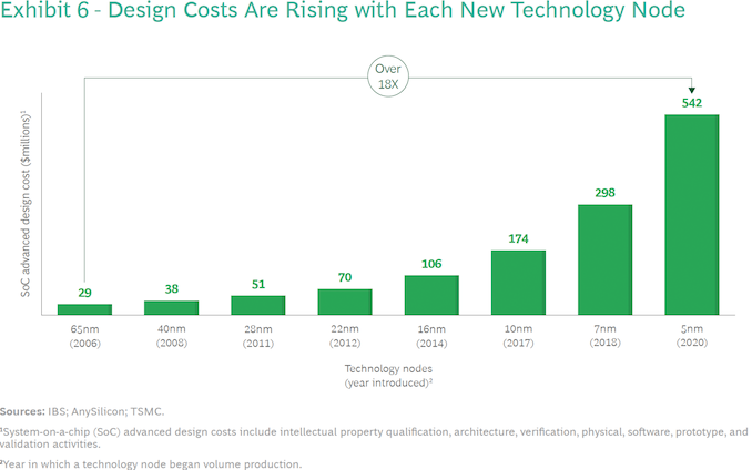
Things get more challenging as the waterfall approach almost excludes backward flows, so people implementing one of the thousands of possible place and route designs have little to zero influence on the architectural or structural design. As a result, the only way to avoid inefficiencies resulting in higher-than-expected costs, lower-than-expected performance, and/or higher-than-expected power consumption is to make different design teams work closer together at all stages. Yet, this gets harder as design cycles get longer.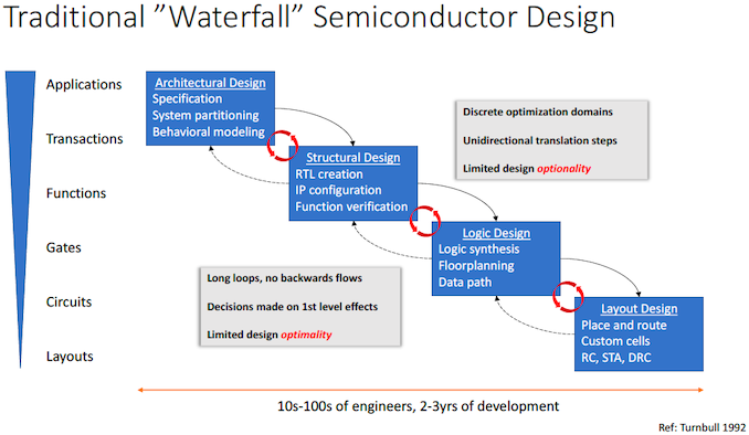
Manufacturing costs at 5 nm and 3 nm production nodes are also noticeably higher than those on previous-generation fabrication technologies. The latest leading-edge manufacturing processes extensively use extreme ultraviolet lithography and more expensive raw materials (e.g., pellicles for photomasks, resists, etc.). Therefore, it gets even more crucial for chip developers to build close-to-perfect designs that are cheaper to make.
In general, the semiconductor industry faces several challenges these days as it needs to cut down development time, maintain (or even reduce) chip development costs, and ensure predictable manufacturing costs. Everything has to be done when the industry faces a deficit of highly skilled engineers.
This is where the Synopsys.ai EDA suite comes into play.
From Scratch to High-Volume Manufacturing
The Synopsys.ai full-stack EDA suite consists of three key applications the DSO.ai AI for chip design: the Synopsys VSO.ai for functional verification, and the TSO.ai for silicon test. The suite is designed to speed up iterative and time-consuming chip design stages using machine learning and reinforcement learning accelerated by modern CPUs and GPUs.
Synopsys has been offering its DSO.ai place and route AI-driven solution for about two years now, and over 100 designs have been taped out using the EDA tool so far. But this time around, the company is looking at fast-tracking all design stages with AI. The software suite can be used at all stages, including simulations, design capture, IP verification, physical implementation, signoff, test, and manufacturing.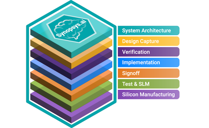
Better Architectures Delivered Faster
Small groups of very talented engineers typically develop microarchitectures, and this stage is considered by many as an intersection of technology and art. In fact, microarchitectures are developed fairly quickly too. Synopsys says that even this stage can be accelerated and improved with AI as artificial as, unlike people, machines can quickly estimate the most efficient architecture parameters and data paths.
The General Manager of Synopsys's Electronic Design Automation Group (EDA), Shankar Krishnamoorthy, states, "The whole process of developing a chip starts with the architecture of the chip and there are a lot of decisions to be made there," He also went on to say "How big does your cache need to be? What kind of interfaces run between your computer and memory? What configurations of memory should you consider, so there are many, many choices there, which an architecture expert would explore rapidly, and then converge on what are the right parameters to implement the chip with. So that process itself is something where AI can be used to rapidly explore that solution space […] and produce an even better result that they may not have gotten to, just because of the compute power that AI can work with."
Another aspect of using AI for microarchitectural explorations is boosting the microarchitecture development capabilities of a given company amid shortages of experienced architects.
Shankar Krishnamoorthy also said, "In cases when you have an expert architect already there, AI is really an assistant. The modern AI techniques are really good at zooming in on the spaces of interest in a very large parameter space by using rewards and penalties. Then you [end up with] a set of menu of choices (such as tradeoffs between power and performance) from which the architect sort of picks the best one for the workload of interest."
Speeding Up IP Verification
Functional and IP verification is a chip design step that takes up a lot of time. It is imperative to test each IP individually and ensure that it functions correctly before integrating them, as the complexity of verification increases exponentially when multiple IPs are combined. Meanwhile, it is crucial to achieving a high level of test coverage for each individual IP.
Nowadays, the common approach for verifying IP involves the designer creating a test benchmark that reflects their verification strategy. This test benchmark is then simulated using conventional simulation techniques, such as constrained random simulation, with the help of a traditional simulator. Achieving high target coverage for a given IP faster is a challenge that can be addressed by the Synopsys VSO.ai, which is part of Synapsys.ai.
"By embedding techniques like reinforcement learning deep into the simulation engine, you can achieve that target coverage" said the head of Synopsys's EDA group. "You say, I need 99% coverage of this IP, you can achieve that target coverage in a much shorter period of time, and using much fewer simulations, because essentially, that reinforcement learning engine that is embedded into the simulation engine is constantly [communication] with the engine that is generating the stimulus."
Renesas confirmed that the Synapsys VSO.ai software could both expand target coverage and speed up the IP verification process.
Takahiro Ikenobe, who is the IP Development Director of the Shared R&D Core IP Division at Renesas, said, "Meeting quality and time-to-market constraints is fast becoming difficult using traditional human-in-the-loop techniques due to the ramp in design complexity. Using AI-driven verification with Synopsys VSO.ai, part of Synopsys.ai, we have achieved up to 10x improvement in reducing functional coverage holes and up to 30% increase in IP verification productivity demonstrating the ability of AI to help us address the challenges of our increasingly complex designs."
Place and Route Done Fast
Speaking of increasingly complex designs, we must remember how hard it is to realize the modern processor's design physically. While modern EDA tools streamline chip development, skilled human engineers are still required to efficiently implement chip floorplan, layout, placement, and routing, utilizing their experience to create efficient designs. Although experienced engineers typically work fast, they are limited in their ability to evaluate hundreds of design options, explore all potential combinations, and simulate tens or even hundreds of different layouts to identify the optimal design within a reasonable timeframe. As a result, in many cases, they implement their best-known methodologies, which may not be the most efficient ones for a particular chip made on a particular production node.
This is when they can use the Synopsys DSO.ai platform that does not need to simulate all the possible ways to place and route a chip but leverages artificial intelligence to evaluate all combinations of architectural choices, power and performance targets, geometries and then simulate a few different layouts to find the one that complies with desired performance, power, area, and cost (PPA) combination in a fraction of the time.
Speaking of simulation, it is important to note that simulating a physically large chip (whether a CPU, GPU or a memory IC) is rather hard to accomplish. Traditionally chip designers used large machines based on CPUs or FPGAs to simulate future chips. Still, recently Synopsys applied GPU acceleration for these workloads and got a several-fold performance uplift.
"If we look at the design of discrete memory, like DRAM or NAND flash, these are very large circuits that need to be simulated for electrical correctness, physical correctness, you know, stress, IR drop all the other types of effects," Krishnamoorthy told us. "Simulation of these very large discrete memory structures is very time-consuming. That's an area where we have successfully applied GPU acceleration in order to achieve several-fold acceleration of the time it takes to simulate these large circuits."
One of the interesting things that Synopsys mentioned during our conversation is that the DSO.ai tool can be used to implement analog circuits — which barely (if at all) scale with each new node — in accordance with new design rules.
"Fundamentally, if you take a PLL, or you take any other type of analog circuit, and you are really not changing the circuit itself, you are migrating it from, let's say, 7 nm to 5 nm or 5 nm to 3 nm," explained the Synopsys executive. "That process of migrating a circuit from one node to another is something that is ripe for automation and ripe for the application of AI. So that is another area where we have applied AI to accelerate that process and cut down the effort and time needed to migrate analog circuits by a significant amount."
According to Synopsys, comparable AI capabilities can simplify the task of transferring chip designs between diverse foundries or process nodes. However, it is worth considering that intricate designs' power, performance, and area characteristics (PPAc) are customized for specific nodes. It remains uncertain whether AI can effectively migrate such a design from one foundry to another while preserving all the key characteristics and whether potential trade-offs of such a migration could be significant.
Synopsys has been offering its DSO.ai platform for about a couple of years, and by now, about 170 chip designs implemented using this EDA tool have been taped out.
"We talked about crossing the 100 tape out milestone in January," said Krishnamoorthy. "We are close to 170 now, so the pace of adoption of that AI-based physical design is really fast among the customer base."
Test and Silicon Lifecycle Management
After a chip was implemented and produced, chip designers need to verify that everything works fine in a process that is somewhat similar to IP verification. This time around, no simulations are involved. Instead, a chip is inserted into a tester device, and specific test patterns are run to confirm that the chip is operating correctly. Therefore, the number of patterns required to test an SoC or an actual system is a major concern for product engineering departments.

The Synopsys TSO.ai tool is designed to help semiconductor companies generate the right test patterns, cut the number of patterns they have to run by 20% to 30% and speed up the silicon test/verification phase. The same test sequences are then used to test all mass-produced chips to ensure they function correctly. The duration of the testing phase directly impacts costs, so it is particularly crucial, especially for high-volume parts.
"We have shown how AI can cut down the total number of patterns needed in order to test circuits by a significant amount," said the Synopsys executive. "We are talking about 20% to 30% type of reductions in test patterns. So that directly translates to cost of test and time on the tester, which is a big deal for companies."
Make Chip Designs Cheaper
Using AI-enabled tools in chip development can speed up their time to market and reduce their development and production costs significantly. Depending on the exact design, Synopsys says we are looking at, at least a 30% - 40% range, and now that hardware development costs of complex chips reach $325 million (at 5 nm) – $900 million (at 3 nm), we are talking about a lot of money.
"Chip costs are obviously hard to estimate," said Shankar Krishnamoorthy. "If I had to guess, I would say, [cost reduction from AI tools usage is] definitely in the 30% to 40% range."
Normally, engineering costs account for around 60% of a chip design cost, whereas compute costs account for approximately 40%. AI can be used to reduce both kinds of costs, according to Synopsys.
When an established company designs a new chip, it comprises 30% to 40% of new IP and 60% to 70% of seasoned IP, said Krishnamoorthy. Traditionally, many engineers migrate IPs from the previous node to the next node, often porting over 60% to 70% of the IPs with minor modifications. However, this is an inefficient use of resources. Instead, by leveraging AI to apply previous learnings to the next generation, the time and resources required to complete these incremental blocks can be dramatically reduced, allowing human engineers to expedite the process.
When it comes to new IP blocks, determining the best way to architect and implement them can be challenging and uncertain, often requiring at least one engineer per block. This approach can impact the number of people needed for the project to converge. However, leveraging AI as an assistant can rapidly explore and learn about new designs and architectures to determine the optimal strategy for implementation, verification, and testing. This can significantly reduce the investment needed for new blocks.
Finally, deploying DSO.ai, VSO.ai, and TSO.ai more widely can reduce the compute cost by enabling more intelligent runs of EDA tools. Rather than relying on a trial-and-error approach and indiscriminately simulating all kinds of circuits, targeted AI-enabled runs can be used to achieve similar results. In the end, compute costs will decrease.
Summary
Synopsys.ai is the industry's first suite of EDA tools that can address all phases of chip design, including IP verification, RTL synthesis, floor planning, place and route, and final functional verification.
The usage of machine learning and reinforcement learning enabled for time-consuming and iterative designed stages such as design space exploration, verification coverage, regression analytics, and test program generation, promises to reduce design costs, lower production costs, increase yields, boost performance, and reduce time-to-market. The set of tools can be particularly useful for chips set to be made on leading-edge nodes, such as 5nm, 3nm, 2nm-class, and beyond.
Furthermore, offloading some of the duties to AI-enabled EDA tools can significantly decrease the load on engineering teams, freeing up their time and minds to develop new features, enhance product differentiation, or design more chips, according to Synopsys.
The company says that top chip designers already use its Synopsys.ai, though not all chips are designed with AI assistance for now.
One of the interesting things that Synopsys pointed out is that its Synapsys.ai software suite mostly relies on CPU acceleration for AI. While select things like large circuit simulations can be accelerated using GPUs, most of the workloads run on Intel CPUs.
More...
-
03-30-23, 08:05 PM #11678
Anandtech: The XPG Fusion Titanium 1600 PSU Review: Outrageous Power, Outstanding Qua
One of the perks of normality largely returning to the PC components market now that the crypto mining bubble has popped has been a big improvement in component availability. Video cards were of course the biggest change there – even if prices on the latest generation remain higher than many would like to see – but crypto farms were also soaking up everything from CPUs and RAM to power supplies. So after a period of almost two years of high-powered PSUs of all flavors being hard to come by, the PSU market is, at last, also returning to normal.
The collapse of crypto mining and underlying improvement of electronics components has also meant that high-power PSU designs have reverted, in a sense, to a more balanced portfolio. PSU vendors are finally making some fresh investments in high-end, high-efficiency designs – PSUs that crypto miners would have never paid the premium for. Especially with the launch of the new ATX 3.0 standard and its 12VHPWR connector, there’s an opportunity for a new generation of PSUs to make their mark while powering the latest video cards.
There are few power supplies where this is more apparent than XPG’s new Fusion Titanium 1600. The sole member of its class thus far, the Fusion is a true flagship-grade PSU with the electronics quality to match. Built by Delta Electronics, the XPG Fusion makes liberal use of Gallium Nitride MOSFETs in order to deliver a monstrous 1600 Watts of power at 80 Plus Titanium levels of efficiency. All the while this will also be one of the first high powered ATX 3.0 power supplies, offering two 12VHPWR connectors – making it suitable to drive two high-end video cards – which is no small feat given the power excursion requirements that come with the ATX 3.0 specification.
To that end, today we are thoroughly exploring everything that makes the XPG Fusion stand out from the crowd. From its oversized chassis to its almost absurd voltage regulation quality, it’s a power supply that few customers will ever need, but certainly makes its mark across the PSU design ecosystem.
More...
-
03-31-23, 12:14 PM #11679
Anandtech: Kioxia and Western Digital Debut 218-Layer 3D NAND: 1Tb TLC with 3.2 GT/s
Kioxia and Western Digital formally introduced their 8th Generation BiCS 3D NAND memory with 218 active layers. The new storage device offers a 1Tb capacity in 3D TLC mode and features 3200 MT/s data transfer speed, a combination that will enable SSD makers to build high-performance, high-capacity drives. To enable such an extreme interface speed, the companies adopted an architecture akin to YMTC's Xtacking.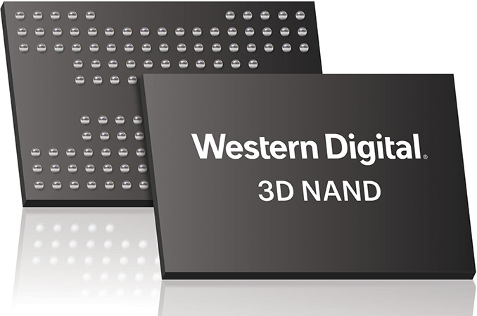
The 218-layer BiCS 3D NAND device jointly developed by Kioxia and Western Digital supports triple-level cell (TLC) and quad-level cell (QLC) configurations to maximize storage density and expand addressable applications. The companies said that the new device embraces their new 'lateral shrink technology to increase bit density by over 50' without elaborating. Considering that the flash memory IC increased the number of active layers by 34%, the claim about a 50% bit density increase indicates that developers also shrank lateral sizes of NAND cells to fit in more of them per layer.
Meanwhile, the 218-layer 3D NAND device features a quad-plane architecture allowing for a higher level of parallelism for programming and read times and increased performance. In addition, the 218-layer 3D TLC device also has a 3200 MT/s (which could provide a 400 MB/s peak read/write speed) input/output interface, which is the highest I/O speed announced so far. High data transfer rates will be handy for high-end client and enterprise SSDs featuring a PCIe 5.0 interface.
The key innovation of the 8th Generation BiCS 3D NAND memory is the all-new CBA (CMOS directly Bonded to Array) architecture that implicates separate production of 3D NAND cell array wafers and I/O CMOS wafers using the most optimal process technologies and then bonding them together to create a final product that offers increased bit density and fast NAND I/O speed. Meanwhile, Kioxia and Western Digital must disclose details about their CBA architecture and whether the I/O CMOS wafers carry other NAND peripheral circuitry, like page buffers, sense amplifiers, and charge pumps.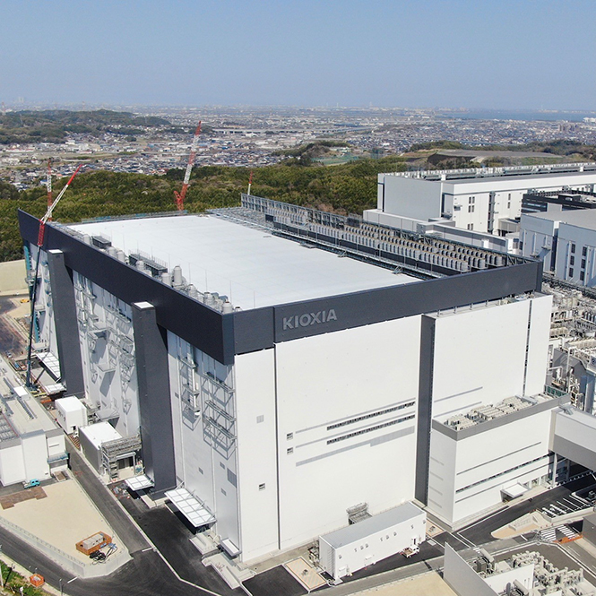
Kioxia and Western Digital Fab 7, Yokkaichi Plant, Japan
Producing memory cells and peripheral circuits separately solves several problems as it allows manufacturers to make them using the most efficient process technologies in their sections of cleanrooms. This brings further benefits as the industry adopts methods like string stacking.
Kioxia said it had started sample shipments of 8th Generation BiCS 3D NAND memory devices to select customers. Still, there is no word when the company expects to initiate volume production of its next-generation flash memory. It is not unusual for companies to announce new types of 3D NAND quarters before they enter mass production, so it is reasonable to expect 8th Gen BICS on the market in 2024.
"Through our unique engineering partnership, we have successfully launched the eighth-generation BiCS Flash with the industry's highest 1-bit density," said Masaki Momodomi, Chief Technology Officer at Kioxia Corporation. "I am pleased that Kioxia's sample shipments for limited customers have started. By applying CBA technology and scaling innovations, we've advanced our portfolio of 3D flash memory technologies for use in various data-centric applications, including smartphones, IoT devices, and data centers."
More...
-
04-04-23, 11:37 AM #11680
Anandtech: AMD Quietly Launches A620 Platform: Sub $100 AM5 Motherboards
AMD has introduced its entry-level A620 platform for AM5 processors. The new platform is designed to power inexpensive PCs that use AMD's CPUs in AM5 packaging based on the Zen 4 microarchitecture and to cut down costs; it omits support for overclocking, PCIe Gen5 connectivity of any kind, and USB 3.2 Gen2x2. Most importantly, base AMD A620-based motherboards will not support higher-wattage CPUs.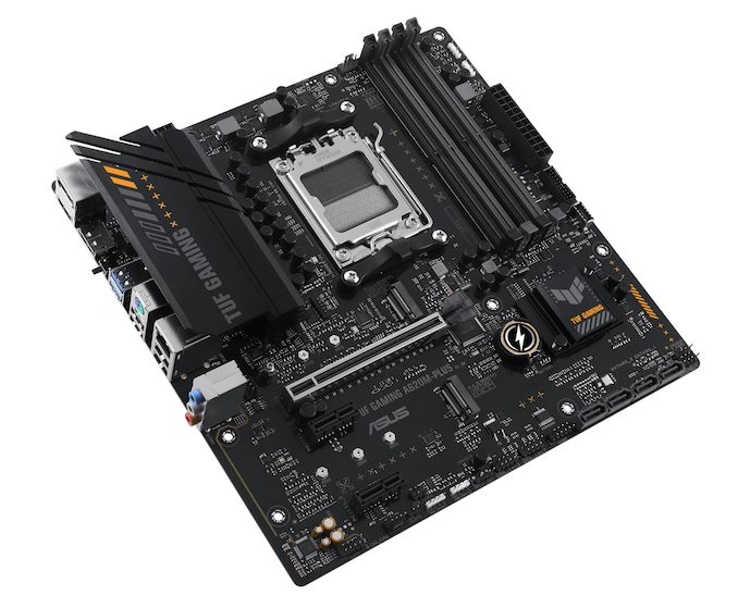
Disabling some connectivity is meant to simplify testing and validation procedures and the design of actual motherboards. On the platform hardware side of matters, the AMD A620 chipset uses the same Promontory 21 silicon as the more expensive B650 and X670 chipsets, but in this case, AMD cut down some of the features supported by silicon. In particular, A620 does not support 10Gbps USB 3.2 Gen2x2, only supports eight PCIe 3.0 lanes (depending on the exact motherboard configuration, the number of enabled lanes may vary), only supports two 10Gbps USB 3.2 Gen2 ports and two 5Gbps USB 3.0 ports.
Regarding motherboard design, AMD also does not mandate its partners to support processors with a TDP higher than 65W, so in many cases (if not most of them) cases A620-based mainboards will not be able to operate Ryzen 7000X or Ryzen 7000X3D CPUs at their full power limits. Our colleagues from Tom's Hardware note that AMD does not explicitly prohibit motherboards makers from supporting high-wattage gaming processors on A620-powered motherboards, but since the platform is meant to be cheap, we can only guess whether there will be many A620 mainboards that feature a sophisticated voltage regulating module for higher-end CPUs.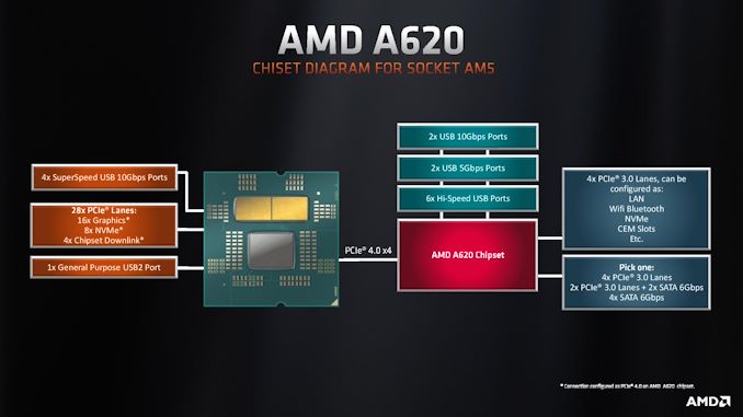
On the bright side, A620-based motherboards support factory-overclocked memory with EXPO profiles up to DDR5-6000; it is uncertain whether further manual memory tuning is permitted.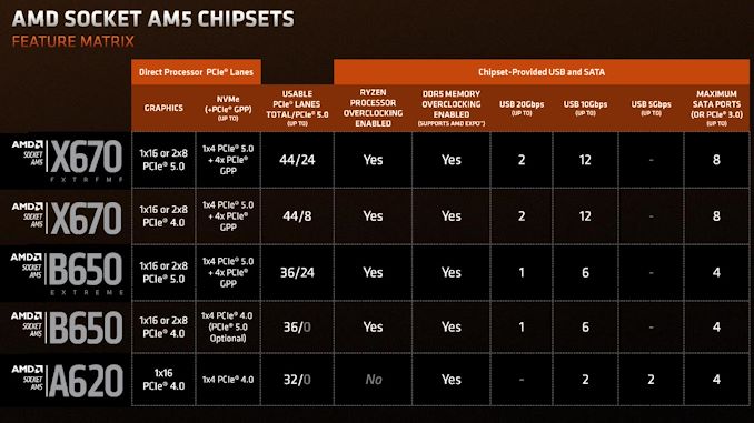
Also, A620 platforms do not support CPU-enabled PCIe Gen5 x4 and x16 interconnections and only feature PCIe Gen4 speeds, which lowers production costs. Yet, they will support four 10Gbps USB 3.2 Gen2 ports enabled by the CPU.
Given the absence of client GPUs supporting a PCIe 5.0 x16 interface, which is unlikely to change for at least a year, and the minimal advantages of PCIe 5.0 x4 SSDs over those with a PCIe 4.0 x4 interface for DirectStorage-enabled games, it seems that opting for PCIe 4.0 speeds instead of PCIe 5.0 for cheap platforms is reasonably practical.
Speaking of cheap AMD AM5 platforms in general, it should be noted that AMD only has three AM5 processors with a 65W TDP, including 12-core Ryzen 9 7900, eight-core Ryzen 7 7700, and six-core Ryzen 5 7600. The latter currently costs $229, which is not particularly cheap.
As for prices of actual A620 motherboards, only ASRock currently offers two of such platforms in the U.S. One costs $86, and another is priced at $100 over at Newegg. Meanwhile, it remains to be seen how cheap or expensive similar A620-based platforms from such makers as Asus, Biostar, Gigabyte, and MSI will be.
Over time AMD will, of course, release inexpensive AM5 APUs with more powerful built-in graphics, and this is when its A620 platform will undoubtedly come in handy. But for now, AMD's Ryzen 7000-series processors mainly target gamers, and the latter are more likely to opt for a Ryzen 7000X chip with enhanced performance and overclocking support or a Ryzen 7000X3D processor with expanded cache for superior single-thread performance, which is going to benefit from more advanced B650-powered motherboards. That said, we can only guess how popular will AMD A620 platform will be before AMD rolls out cheaper AM5 processors.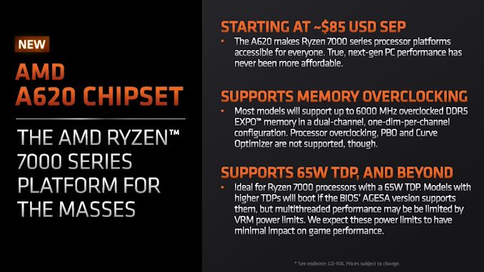
More...


 Quote
QuoteThread Information
Users Browsing this Thread
There are currently 20 users browsing this thread. (0 members and 20 guests)


Bookmarks