

Results 11,701 to 11,710 of 12091
Thread: Anandtech News
-
04-21-23, 10:36 AM #11701
Anandtech: SK hynix Now Sampling 24GB HBM3 Stacks, Preparing for Mass Production
When SK hynix initially announced its HBM3 memory portfolio in late 2021, the company said it was developing both 8-Hi 16GB memory stacks as well as even more technically complex 12-Hi 24GB memory stacks. Now, almost 18 months after that initial announcement, SK hynix has finally begun sampling its 24GB HBM3 stacks to multiple customers, with an aim towards going into mass production and market availability in the second half of the year. All of which should be a very welcome development for SK hynix's downstream customers, many of whom are chomping at the bit for additional memory capacity to meet the needs of large language models and other high-end computing uses.
Based on the same technology as SK hynix's existing 16GB HBM3 memory modules, the 24GB stacks are designed to further improve on the density of the overall HBM3 memory module by increasing the number of DRAM layers from 8 to 12 – adding 50% more layers for 50% more capacity. This is something that's been in the HBM specification for quite some time, but it's proven difficult to pull off as it requires making the extremely thin DRAM dies in a stack even thinner in order to squeeze more in.
Standard HBM DRAM packages are typically 700 – 800 microns high (Samsung claims its 8-Hi and 12-Hi HBM2E are 720 microns high), and, ideally, that height needs to be maintained in order for these denser stacks to be physically compatible with existing product designs, and to a lesser extent to avoid towering over the processors they're paired with. As a result, to pack 12 memory devices into a standard KGSD, memory producers must either shrink the thickness of each DRAM layer without compromising performance or yield, reduce the space between layers, minimize the base layer, or introduce a combination of all three measures.
While SK hynix's latest press release offers limited details, the company has apparently gone for thinning out the DRAM dies and the space between them with an improved underfill material. For the DRAM dies themselves, SK hynix has previously stated that they've been able to shave their die thickness down to 30 microns. Meanwhile, the improved underflow material on their 12-Hi stacks is being provided via as part of the company's new Mass Reflow Molded Underfill (MR-MUF) packing technology. This technique involves bonding the DRAM dies together all at once via the reflow process, while simultaneously filling the gaps between the dies with the underfill material.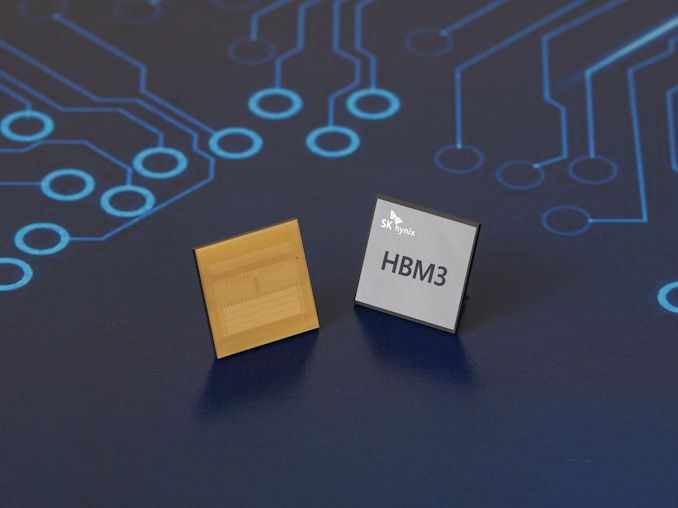
SK hynix calls their improved underfill material "liquid Epoxy Molding Compound", or "liquid EMC", which replaces the older non conductive film (NCF) used in older generations of HBM. Of particular interest here, besides the thinner layers this allows, according to SK hynix liquid EMC offers twice the thermal conductivity of NCF. Keeping the lower layers of stacked chips reasonably cool has been one of the biggest challenges with chip stacking technology of all varieties, so doubling the thermal conductivity of their fill material marks a significant improvement for SK hynix. It should go a long way towards making 12-Hi stacks more viable by better dissipating heat from the well-buried lowest-level dies.
Assembly aside, the performance specifications for SK hynix's 24GB HBM3 stacks are identical to their existing 16GB stacks. That means a maximum data transfer speed of 6.4Gbps/pin running over a 1024-bit interface, providing a total bandwidth of 819.2 GB/s per stack.
Ultimately, all the assembly difficulties with 12-Hi HBM3 stacks should be more than justified by the benefits that the additional memory capacity brings. SK hynix's major customers are already employing 6+ HBM3 stacks on a single product in order to deliver the total bandwidth and memory capacities they deem necessary. A 50% boost in memory capacity, in turn, will be a significant boon to products such as GPUs and other forms of AI accelerators, especially as this era of large language models has seen memory capacity become bottlenecking factor in model training. NVIDIA is already pushing the envelope on memory capacity with their H100 NVL – a specialized, 96GB H100 SKU that enables previously-reserved memory – so it's easy to see how they would be eager to be able to provide 120GB/144GB H100 parts using 24GB HBM3 stacks.
Source: SK Hynix
More...
-
04-24-23, 11:54 AM #11702
Anandtech: MSI Addresses CPU Voltages on AM5 Motherboards for Ryzen 7000X3D Processor
In response to recent reports of AMD's Ryzen 7000X3D processors being damaged, MSI has announced a wave of firmware updates to address potential issues. The highlight of MSI's new wave of BIOS versions for its AM5 motherboards is that the company is further locking down the voltage controls for X3D chips, removing support for positive offset voltages. Going forward, it will only be possible to use negative offset voltages on X3D chips, ensuring that the sensitive V-Cache-equipped X3D chips can't be overvolted and put at risk of damage.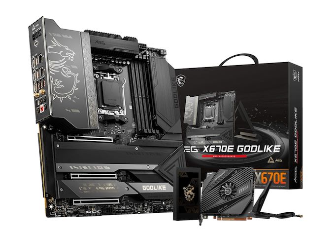
Over the last couple of days, there has been concern across various social media platforms, such as Reddit, about reports of AMD's Ryzen 7000X3D processors spontaneously 'burning out.' Multiple users have posted issues where their Ryzen 7000X3D processors with 3D V-Cache have been dying – and curiously, all when using ASUS motherboards.
Perhaps one of the most recognizable images over the last few days has been via a Reddit post by Speedrookie. In the image above, the user uploaded a photo that shows his AMD Ryzen 7800X3D and ASUS ROG Strix X670E-E Gaming motherboard with very noticeable scorch marks within the CPU socket itself, as well as a very large bulging on the CPU contact pads.
There is little concrete information about where the issue lies – whether it's even a systemic issue, or just a statistical fluke – but it would seem that MSI considers it an important enough matter to take immediate action via new firmware versions for its AM5 motherboards, including those with X670E, X670E, B650, and A620 chipsets.
Announced via a post on Reddit, the company is releasing new BIOSes for all of its AM5 platform motherboards. The new firmware from MSI specifically targets overvolting Ryzen 7000X3D CPUs or restricting the ability to do this. The new firmware from MSI essentially locks down any options or settings related to voltage adjustment. This includes blocking positive voltage offsets, as well as direct voltage adjustment. Consequently, with the new BIOSes it's only possible to use offering negative offset voltage settings on X3D chips
These updates don't just impact the firmware itself, but MSI has also restricted overvolting through its MSI Center application. So, much like their firmware, MSI Center won't allow users to add any additional CPU VCore to the processor when used on any the Ryzen 7000X3D processors such as the Ryzen 9 7950X3D and the Ryzen 7 7800X3D which we've both reviewed recently.
Aside from the MSI Pro X670-P WIFI and MAG B650M Mortar WIFI motherboards, the rest of MSI's line-up has new firmware available for users to install and flash over the current BIOS version. MSI states that the remaining two boards will soon have a new firmware version. It should also be noted that on the official product pages for each motherboard and its corresponding BIOS version, these new BIOSes are listed as 'Beta'.MSI AM5 Motherboard New BIOS Versions (as of 04/24) AnandTech BIOS Version
(Click to Download)Price at Amazon
($)MEG X670E Godlike E7D68AMS.151 $1284 MEG X670 Ace E7D69AMS.181 $700 MPG X670E Carbon WIFI E7D70AMS.171 $361 MAG X670E Tomahawk WIFI E7E12AMS.131 $310 Pro X670-P WIFI Coming Soon $264 MPG B650 Carbon WIFI E7D74AMS.151 $300 MPG B650 Edge WIFI E7E10AMS.161 $260 MPG B650I Edge WIFI E7D73AMS.131 $311 MAG B650 Tomahawk WIFI E7D75AMS.161 $219 MAG B650M Mortar WIFI Coming Soon Pro B650-P WIFI E7D78AMS.151 $200 Pro B650M-A WIFI E7D77AMS.181 $180 Pro B650M-A E7D77AMS.181 - Pro A620M-E E7E28AMS.121 $108
Meanwhile, for users still looking to squeeze a bit more out of their X3D processors, MSI is directing users to utilize the Enhanced Mode Boost option within the firmware, which essentially optimizes the Precision Boost Overdrive (PBO) settings without making manual voltage adjustments.
As the situation develops, we expect to hear more from other vendors and users expressing issues. In the meantime, if you use an MSI AM5 motherboard with a Ryzen 7000X3D processor, these new BIOSes likely warrant a good look and a quick installation.
More...
-
04-25-23, 03:00 AM #11703
Anandtech: Asustor Launches Flashstor NAS: Up To 12 M.2 Slots & 10GbE Connectivity
Asustor, one of the more popular NAS manufacturers, has announced the company's new Flashtor series. The Flashtor lineup, which currently consists of the Flashtor 6 (FS6706T) and Flashtor 12 Pro (FS6712X), caters to content creators and enthusiasts, offering a rich feature set that includes the capacity to house up to 12 PCIe 3.0 M.2 slots for NVMe SSDs, fast 10GbE connectivity and HDMI 2.0b port that supports 4K displays at 60 Hz. It's the first time the brand has launched a NAS featuring all-M.2 NVMe SSD storage.
The Flashtor series arrives with a black and very console-looking exterior. The aesthetics may be a refreshing departure from the typical NAS look for some. The Flashtor 6 and Flashtor 12 Pro have identical dimensions. Both measure 12.1 x 7.6 x 1.9 inches (308.26 x 193 x 48.3 mm). The weight varies slightly, though. The Flashtor 6 weighs 2.98 pounds (1.35 kilograms), while the Flashtor 12 Pro checks in at 3 pounds (1.37 kilograms).
The Flashtor 6 and Flashtor 12 Pro leverages Intel's Celeron N5105 (Jasper Lake) processor. The 10nm chip features four Tremont cores without Hyper-Threading that operate with a 2 GHz base clock and 2.9 GHz boost clock. The 10W processor doesn't have demanding cooling requirements, making it a common choice among NAS vendors. Asustor pairs the Celeron N5105 with a 4 GB SO-DIMM DDR4-2933 memory module. Regardless of the model, the Flashtor devices come with two SO-DIMM DDR4 memory slots and allow up to 16 GB (2 x 8 GB), the maximum capacity supported on the Celeron N5105. Asustor's NAS also has 8 GB of onboard eMMC storage.
The Flashtor 6 and Flashtor 12 Pro differs in storage capacity and connectivity options. The former has six PCIe 3.0 M.2 slots for M.2 2280 drives, whereas the latter has 12. The NAS supports RAID 0, 1, 5, 6, and 10 arrays. In addition, Asustor designed specific air ducts and a small 80 mm cooling fan to keep the drives cool. The included M.2 heatsinks help with heat dissipation. While the Flashtor series are based on NVMe storage, consumers can still utilize hard drives when they need vast amounts of raw storage. However, consumers will need to employ the help of the AS6004U, a four-bay NAS storage capacity expander from Asustor that retails for $329. The AS6004U connects to the Flashtor devices through a standard USB 3 port.Asustor Flashtor NAS Specifications Component Flashtor 6 Flashtor 12 Pro CPU Intel Celeron N5105 Intel Celeron N5105 RAM 4 GB DDR4-2933 SO-DIMM 4 GB DDR4-2933 SO-DIMM Flash Memory 8 GB eMMC 8 GB eMMC Storage 6 x PCIe 3.0 M.2 Slots 12 x PCIe 3.0 M.2 Slots Networking 2 x 2.5 Gigabit Ethernet 1 x 10 Gigabit Ethernet I/O 2 x USB 3.2 Gen 2x1
2 x USB 2.0
1 x HDMI 2.0b
1 x S/PDIF2 x USB 3.2 Gen 2x1
2 x USB 2.0
1 x HDMI 2.0b
1 x S/PDIFPower Adapter 65 W 90 W Power Consumption 18.2 W 26 W Noise Level 18.7 dB 18.7 dB Dimensions (inches) 12.1 x 7.6 x 1.9 12.1 x 7.6 x 1.9 Weight 2.98 lbs (1.35 kg) 3.0 lbs (1.37 kg) Starting Price (USD) $449 $799
Asustor equipped the Flashtor 6 with two 2.5 Gigabit Ethernet ports with read and write speeds up to 590 MB/s and 583 MB/s, respectively, in an SMB multichannel (RAID 5) environment. In contrast, the Flashtor 12 Pro only has a 10 Gigabit Ethernet port but flaunts read and write speeds up to 1,181 MB/s and 1,027 MB/s, respectively, in Windows with a RAID 5 array. It's important to highlight that Asustor achieved these performance numbers in the company's lab with avant-garde systems and optimized network settings. The consumer mileage will vary.
Gallery: Asustor Flashtor Series


Only the Flashtor 6 supports Wake on LAN (WoL) and Wake on WAN (WoW) since the Flashtor 12 Pro only supports the former. In addition, the Flashtor series provides consumers with two USB 3.2 Gen 2x1 ports and two USB 2.0 ports for connecting external devices. As for multimedia, the NAS devices supply one HDMI 2.0b port for video and one S/PDIF output for lossless audio.
Asustor bundles a 65 W power adapter with the Flashtor 6 and a 90 W unit with the Flashtor 12 Pro. According to the brand, the Flashtor 6 pulls around 18.2 W during operation, and the Flashtor 12 Pro consumes around 26 W. The noise levels aren't outrageous, either. Asustor rates the Flashtor series with a noise level of 18.7 dB.
The Flashtor 6 and Flashtor 12 Pro retail for $449 and $799, respectively. Asustor backs the Flashtor series with a three-year warranty.
More...
-
04-25-23, 04:24 PM #11704
Anandtech: ASUS Issues Statement on Ryzen 7000X3D Processor Issues, Possible Voltage
Yesterday we reported that MSI announced a wave of firmware updates designed to address and alleviate potential issues with users on AM5 using AMD's Ryzen 7000X3D processors with 3D V-Cache. One of the main changes with MSI's latest UEFI firmware for AM5 included voltage restrictions when using Ryzen 7000X3D series CPUs so that these chips couldn't be overvolted as the V-Cache packaging is somewhat sensitive to additional power.
Further to MSI's announcement, ASUS has released a statement to experienced engineer and extreme overclocker Roman 'Der8auer' Hartung, which addresses the potential issue with using AMD's EXPO memory profiles in conjunction with the Ryzen 7000X3D series chips. One of the key elements that seemingly surrounds the problem is the use of AMD's EXPO memory overclocking profiles.
ASUS's Director of Global Product Marketing and Technical Marketing, Rajinder Gill, said in a statement to Der8auer, "The EFI updates posted on Friday contain some dedicated thermal monitoring mechanisms we've implemented to help protect the boards and CPUs. We removed older BIOSes for that reason and also because manual Vcore control was available on previous builds." Rajinder also said, "We're also working with AMD on defining new rules for AMD Expo and SoC voltage. We'll issue new updates for that ASAP. Please bear with us."
Looking at the narrative of the statement provided to Der8uaer from Rajinder, we can confirm that ASUS has indeed removed older iterations of its firmware for its AM5 motherboards. Looking at the EMEA side of things, at the time of writing, the latest firmware update to be posted on the ASUS product pages is dated 04/21/2023, which indicates ASUS recently updated the firmware, but the update isn't the latest one in question.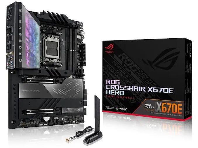
ASUS ROG Crosshair X670E Hero AM5 Motherboard for AMD Ryzen 7000 Series CPUs
The one thing these issues have in common is that AMD's EXPO memory profiles have been applied, claims Roman 'Der8auer' Hartung, and even highlighted that his Ryzen 9 7900X processor also fell foul the the 'bulging issue.' This is particularly interesting as this isn't an X3D series chip with 3D V-Cache, although we're not aware of any other reports of non-X3D Ryzen 7000 chips being affected at this time.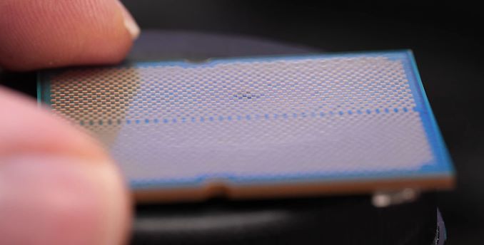
Roman 'Der8auer' Hartung's Ryzen 9 7900X also has a bulge.
Enabling EXPO memory profiles on Ryzen 7000 processors does several things to the processor that pushes it beyond the technical specification of the chip. Chief among these is raising the SoC voltage and some other primary voltages, such as VDDIO, which are used to feed the IOD. Like any ASIC, there are limits to how high voltages can be safely pushed, and this is one theory behind the cause of the recent run of damaged Ryzen reports. Though how this might be connected to the issue being centered around Ryzen X3D chips – where the voltage-sensitive V-Cache is on the CCDs and their separate voltage plane – is unclear at this time.
In any case, this does underscore why AMD's EXPO memory overclocking profiles void the warranty on these chips, as there's more to EXPO than just ramping up memory frequencies and applying more voltage to the DRAM itself.
Further to Rajinder's statement given to Der8auer, ASUS's Senior Technical Marketing Manager, Juan Jose Guerrero, posted the following statement on Twitter Tuesday afternoon:
"Several AMD Ryzen 7000X3D owners have reported CPU and motherboard failures. We acknowledge the incidents/issues and have been communicating with AMD to analyze the possible causes. We have also contacted affected users to provide support and collect additional information.
Ryzen 7000X3D processors do not allow for CPU ratio or CPU core voltage tuning (CPU overclocking) but do allow for performance tuning and DRAM overclocking via PBO2 and EXPO memory. To support EXPO and/or memory overclocking at DDR5-6000 and beyond, SoC voltage has to be sufficiently increased to ensure compatibility and stability. The amount of voltage required varies between CPU samples. Some processors are more sensitive to overvoltage than others, and some are capable at running higher memory frequencies without needing as much voltage.
As confirmed with AMD, any intentional manipulation of these settings can damage the processor, socket, and motherboard. To mitigate this, we have been working with AMD to define new rules for EXPO memory and SoC voltage. To help protect the CPU and motherboard, we are issuing new EFI updates to limit the maximum available SoC voltage to 1.3V.
We recommend updating your motherboard UEFI BIOS to the latest release. Please also ensure the CPU is cooled adequately. Our recommendation is to use at least a 240mm AIO liquid cooler or high-performance air cooler. If you have been affected, please do not hesitate to contact ASUS support for your region.
As we mentioned in our article yesterday about MSI addressing CPU voltage on their own AM5 motherboards, vendors are looking to address any more potential issues, following a small-but-concerning number of reports circulating on Reddit that their Ryzen 7000X3D processors are burning out and killing the motherboard in the process. ASUS's statement and the summary of the firmware on the official product page indicate that ASUS is worried about SoC voltage, and as such, the new firmware locks it down to 1.30 V. Which ASUS states is to 'protect the CPU and motherboard.'
On the Chinese product page for the ROG Crosshair X670E Extreme, the firmware has been updated as of today (at the time of writing) to 04/25/2023, and the firmware version in question (1302) does seemingly address the SoC voltage.
Screenshot of the ROG Crosshair X670E Extreme BIOS/Support page on the official product page (China).
Further to ASUS's and MSI's statements, AMD has officially responded with a statement of their own:
It reads, "We are aware of a limited number of reports online claiming that excess voltage while overclocking may have damaged the motherboard socket and pin pads. We are actively investigating the situation and are working with our ODM partners to ensure voltages applied to Ryzen 7000X3D CPUs via motherboard BIOS settings are within product specifications. Anyone whose CPU may have been impacted by this issue should contact AMD customer support."
Of course, these issues of Ryzen 7000X3D series processors burning out aren't just limited to those using MSI and ASUS motherboards. Since the initial reports, users have reported additional issues on various models and brands across threads on Reddit. The potential for damage is one of the primary reasons AMD locked down the X3D series processors so that users couldn't manually overclock them. Even the first iteration, the Ryzen 7 5800X3D, was also locked down.
One thing remains clear: AMD and its motherboard partners are now officially investigating the matter, and users with affected Ryzen 7000 CPUs are advised to contact AMD customer support directly.
More...
-
04-25-23, 04:24 PM #11705
Anandtech: AMD Issues Official Statement on Reported Ryzen 7000 Burnout Issues
Yesterday we reported that MSI announced a wave of firmware updates designed to address and alleviate potential issues with users on AM5 using AMD's Ryzen 7000X3D processors with 3D V-Cache. One of the main changes with MSI's latest UEFI firmware for AM5 included voltage restrictions when using Ryzen 7000X3D series CPUs. Further to recent reports of users with AMD Ryzen 7000X3D processors experiencing damage to their chip and motherboard socket, we reached out to AMD this morning to seek clarification. AMD has just responded with an official statement concerning the current problem.
The statement directly from AMD is as follows:
"We are aware of a limited number of reports online claiming that excess voltage while overclocking may have damaged the motherboard socket and pin pads. We are actively investigating the situation and are working with our ODM partners to ensure voltages applied to Ryzen 7000X3D CPUs via motherboard BIOS settings are within product specifications. Anyone whose CPU may have been impacted by this issue should contact AMD customer support."
As the statement clarifies, AMD themselves are investigating the issue that users have been experiencing, which has been reported on through various channels such as social media and Reddit. This is further to MSI, which launched new firmware yesterday, and ASUS announced new firmware today for users with AMD Ryzen 7000X3D processors, such as the Ryzen 9 7950X3D and the Ryzen 7 7800X3D. The new firmware specifically limits the SoC voltages applied so that these critical limits aren't breached when users enable AMD EXPO memory profiles on supported DRAM.
While AMD hasn't officially confirmed the problem regarding the burnt pads on the Ryzen 7000X3D series processors and the burnt pins within the motherboard socket, AMD is actively looking to resolve this issue. One theory thus far is that the issue is being triggered when users are enabling AMD EXPO memory profiles – which, much like Intel's XMP counterpart, is technically a form of overclocking and officially voids the product warranty. Given the rollout of new firmware, which targets SoC voltages and restricts them, all things point towards voltages and overclocking said processors, which are, by default, multiplier and CPU VCore locked.
AMD is actively working with motherboard vendors such as MSI, ASUS, GIGABYTE, and ASRock to roll out the new firmware. AMD also specifies that if users have a Ryzen 7000X3D processor affected by this problem, to contact AMD customer support directly.
Image source: Speedrookie/Reddit
More...
-
04-26-23, 08:23 AM #11706
Anandtech: AMD Releases Ryzen Z1 Series: Zen 4 & RDNA 3 Come To Handheld Game Console
AMD has announced the Ryzen Z1 series of high-performance processors for handheld PC gaming consoles. The latest Ryzen Z1 chips wield Zen 4 cores and RDNA 3 graphics, a familiar combination that AMD uses for its current mobile Ryzen 7040HS series (Phoenix) processors. And while the chipmaker hasn't officially announced any lower power Phoenix chips yet (e.g. Ryzen 7040U series), given the similarities in the feature set of the Ryzen Z1 family and the Phoenix silicon, the Ryzen Z1 series appears to be a custom-tailored Phoenix SKU that prioritizes energy efficiency for handheld gaming devices .The lead customer for the Ryzen Z1 will be Asus, who will be using it in their upcoming ROG Alloy.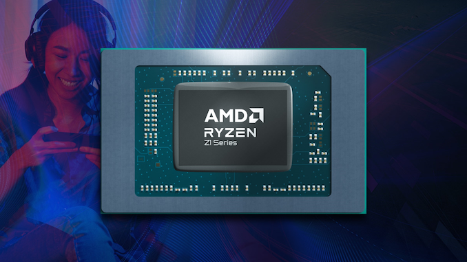
The Ryzen Z1 series is being introduced with two SKUs. The top-tier Ryzen Z1 Extreme has eight Zen 4 CPU cores – the maximum found on Phoenix – while the vanilla Ryzen Z1 cuts that down to six CPU cores. Meanwhile on the graphics side of matters, the Ryzen Z1 Extreme flaunts 12 RDNA 3 architecture compute units, again aligning with the max number found on Phoenix silicon. It's vanilla Z1 counterpart, on the other hand, will ship with just 4 CUs enabled, one-third as many as on the flagship part.
Both chips benefit from a 16 MB L3 cache, while the Ryzen Z1 Extreme has 2 MB more L2 cache due to its additional CPU cores. In any event, the Ryzen 1 and Ryzen Z1 Extreme possess strong computing performance thanks to the high CPU core count and the usage of AMD's latest Zen 4 cores. A hexa-core processor should suffice for handheld gaming, and either Ryzen Z1 processor will certainly outperform AMD's older custom quad-core Zen 2 SoC (Aerith) that powers Valve's Steam Deck.
Hardware unit counts aisde, AMD isn't revealing the clock speeds for the two 4nm processors. Curiously, an embargoed report published by The Verge has quoted "up to" 8.6 TFLOPS and 2.6 TFLOPS graphics performance respectively, based on AMD's engineering projections. But these figures have been removed from the deck AMD has since been sending around to the rest of the press. If these figures do turn out to be reasonably close to what the final shipping silicon can hit, then that would mean we'd be looking at peak GPU clockspeeds of around 2.8GHz and 2.6GHz respectively, which is just a bit lower than what the Ryzen 7040HS chips run at.AMD Ryzen Z1 Specifications AnandTech Cores
ThreadsBase
FreqTurbo
FreqL2
CacheL3
CacheGPU TDP Ryzen Z1 Extreme 8/16 ? ? 8 MB 16 MB 12 RDNA 3 CUs 15 - 30 W Ryzen Z1 6/12 ? ? 6 MB 16 MB 4 RDNA 3 CUs 15 - 30 W
The Ryzen Z1 series chips will support a maximum TDP of 30 Watts, which happens to be the same top power target as AMD's mobile Ryzen U-series chips. Meanwhile, although this wasn't in AMD's press deck or press release, AMD's Ryzen Z1 product page lists a minimum TDP of 15 Watts. Though it's worth noting that unlike TDP maximums, TDP minimums are not a hard floor or ceiling for mobile processors. Chips can be configured to run even less when it's called for, depending on what the customer desires.
Just to offer a comparison here, Aerith's TDP is between 4 W and 15 W, meaning the Z1 series certainly offers a good deal larger power range for customers to play with. At its top TDP, such a configuration would quickly blow through the battery in any handheld device, but for docked devices it's very feasible. As for handheld mode, it's far more likely that we'll see Z1 chips clocked relatively low to conserve precious power.
Being that this is an AMD product designed for PC-like devices, it has access to all AMD graphics technologies, including Radeon Chill, which helps improve battery life by adjusting frame rates based on the movements in the game. This also means that FSR will be on the table on a game-by-game basis, and RSR as a less optimal universal solution.
Gallery: AMD Ryzen Z1 Series Slide Deck


AMD provided some benchmarks for the Ryzen Z1 series utilizing the Asus ROG Ally. As usual, throw a pinch of salt over vendor-provided benchmarks. The device used here also had 16 GB of LPDDR5 memory and a Micron 500 MB SSD. It's important to highlight that AMD put the Asus ROG Alloy in turbo mode for its benchmarks, which means that the Ryzen Z1 series processors were operating at power levels up to 30 Watts.
AMD's results show the Ryzen Z1 Extreme delivers average frame rates above 60 FPS in most titles. However, the chipmaker tested with the lowest settings at a mix of 1080p and 720p upscaled with RSR to hit those figures. The Ryzen Z1's performance wasn't bad, but the two chips' delta was perceptible. The difference spans between 6% and 73%. Zen 4-based processors took a significant performance hit at native 1080p resolution on the lowest settings. As expected, the Ryzen Z1 struggled in multiple titles and didn't hit the 60 FPS mark.
Asus has first dibs on the Ryzen Z1 series; however, more competitors powered by the 4nm Ryzen Z1 chips should arrive down the road. Asus' ROG Ally will be the first handheld gaming console to feature AMD's Ryzen Z1 Extreme processor, with the company set to share more information on the handheld (including pricing) on May 11.
More...
-
04-27-23, 12:11 AM #11707
Anandtech: TSMC Details 3nm Evolution: N3E On Schedule, N3P and N3X To Deliver 5% Per
Alongside some new announcements for their 2nm process node plans, TSMC has also released a progress and roadmap update for their N3 family process technologies at today's 2023 North American Technology Symposium. TSMC's final generation of FinFET-based process nodes, the N3 family is expected to remain around in some shape or form for many years to come as the densest node available for customers who don't need a more cutting-edge GAAFET-based process.
TSMC's big roadmap updates on the N3 front were with N3P and its high performance variant, N3X. As revealed today by TSMC, N3P will be an optical shrink of N3E, offering enhanced performance, reduced power consumption, and increased transistor density compared to N3E, all while maintaining compatibility with N3E's design rules. Meanwhile, N3X will wed extreme performance with 3nm-class densities, offering higher clockspeeds for high performance CPUs and other processors.
N3E: 3nm for Everyone Is on Schedule
As a quick refresher, TSMC's N3 (3nm-class) family of process technologies is comprised of several variants, including baseline N3 (aka N3B), relaxed N3E with reduced costs, N3P with enhanced performance and chip density, and N3X with higher voltage tolerances. Last year the company also talked about N3S with maximized transistor density, but this year the company remains tight lipped about this node and it is not mentioned anywhere in its slides.
TSMC's vanilla N3 node features up to 25 EUV layers, with TSMC using EUV double-patterning on some of them to make for higher logic and SRAM transistor density than N5. EUV steps are expensive in general, and EUV double patterning drives those costs up further, which is why this fabrication process is only expected to be used by a handful of customers who are not as concerned about the high outlay required.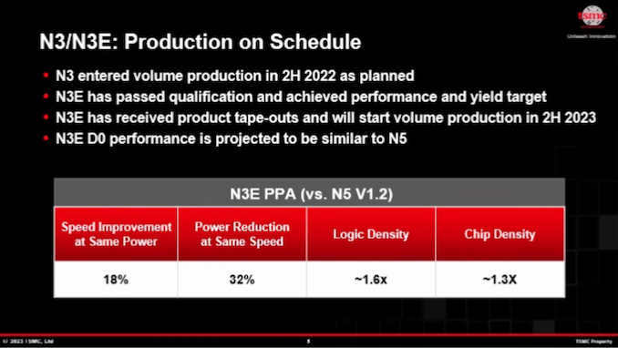
The majority of TSMC's clients interested in a 3nm-class process are expected to use the relaxed N3E node, which according to TSMC is on schedule and achieving their performance targets. N3E uses up to 19 EUV layers and does not rely on EUV double patterning at all, reducing its complexity and costs. The trade-off is that N3E offers lower logic density than N3, and it has the same SRAM cell size as TSMC's N5 node, making it somewhat less attractive to those customers who are driving for density/area gains. Overall, N3E promises a wider process window and better yields, which are two crucial metrics in chip fabrication.Advertised PPA Improvements of New Process Technologies
Data announced during conference calls, events, press briefings and press releasesTSMC N3
vs
N5N3E
vs
N5Power -25-30% -32% Performance +10-15% +18% Logic Area
Reduction* %
Logic Density*0.58x
-42%
1.7x0.625x
-37.5%
1.6xSRAM Cell Size 0.0199µm² (-5% vs N5) 0.021µm² (same as N5) Volume
ManufacturingLate 2022 H2 2023
"N3E will be better than N3 in terms of yield, process complexity, which directly translating into [wider] process window," said Kevin Zhang, Vice President of Business Development at TSMC.
N3P: Higher Performance, Higher Transistor Density
Following N3E, TSMC will continue to optimize the N3 family's transistor density with N3P, which will build on N3E by offering improved transistor characteristics. The refined process node will allow chip designers to either increase performance by 5% at the same leakage or reduce power by 5% ~ 10% at the same clocks. The new node will also increase transistor density by 4% for a 'mixed' chip design, which TSMC defines as a chip consisting of 50% logic, 30% SRAM, and 20% analog circuits.
As part of their discussion on N3P, TSMC stressed that the density improvement was achieved by adjusting the optical performance of its scanners. So it is likely that TSMC will be able to shrink all types of chip structures here, which will make N3P an attractive node for SRAM-intensive designs.
"N3P is a performance boost, it has a 5% higher performance, at least a 5% higher than N3E," explained Zhang. It also has the 2% optical shrink, which bring transistor density to 1.04x."
Since N3P is an optical shrink of N3E, it will preserve N3E's design rules, enabling chip designers to quickly reuse N3E IP on the new node. Consequently, N3P is also projected to be one of TSMC's most popular N3 nodes, so expect IP design houses like Cadence and Synopsys to offer a variety of IP for this process technology, reaping the benefits of forward compatibility with existing N3E in the process. TSMC says that N3P will be production ready in the second half of 2024.Advertised PPA Improvements of New Process Technologies
Data announced during conference calls, events, press briefings and press releasesTSMC N3
vs
N5N3E
vs
N5N3P
vs
N4EN3X
vs
N3PPower -25-30% -32% -5% ~ 10% higher Performance +10-15% +18% +5% +5%
Fmax @ 1.2VChip Density ? ? SRAM Cell Size 0.0199µm² (-5% vs N5) 0.021µm² (same as N5) ? ? Volume
ManufacturingLate 2022 H2 2023 H2 2024 2025
N3X: Maximum Performance and Density
Finally, for developers of high-performance computing applications like CPUs and GPUs, TSMC has for the past few generations been offering its X family of high voltage, performance-focused nodes. As disclosed at last year's event, the N3 family will be getting its own X variant with the aptly named N3X node.
Compared to N3E, N3X is projected to offer at least 5% higher clockspeeds compared to N3P. This is being accomplished by making the node more tolerant of higher voltages, allowing chip designers to crank up the clockspeeds in exchange for higher overall leakage.
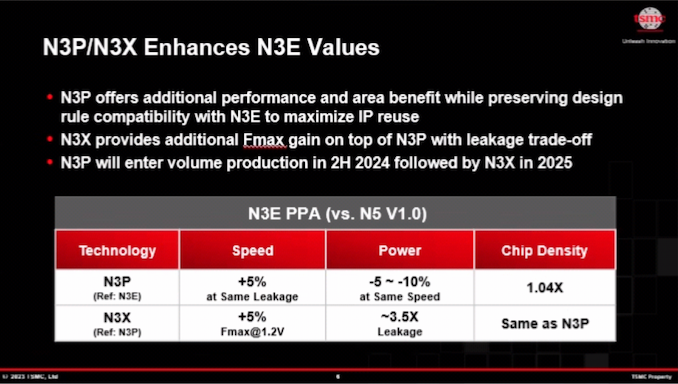
TSMC claims that N3X will support voltages of (at least) 1.2v, which is a fairly extreme voltage for a 3nm-class fabrication process. The leakage cost, in turn, is significant, with TSMC projecting a whopping 250% increase in power leakage over the more balanced N3P node. This underscores why N3X is really only usable for HPC-class processors, and that chip designers will need to take extra care to keep their most powerful (and power-hungry) chips in check.
As for transistor density, N3X will offer the same density as N3P. TSMC has not commented on whether it will also maintain design rule compatibility with N3P and N3E, so it will be interesting to see what ends up happening there.
The final N3 family node in TSMC's current roadmap, the company says that that N3X will be production ready in 2025.
More...
-
04-27-23, 12:11 AM #11708
Anandtech: TSMC Outlines 2nm Plans: N2P Brings Backside Power Delivery in 2026, N2X A
At its 2023 North American Technology Symposium today, TSMC has disclosed additional details about its plans for its forthcoming N2 2nm-class production nodes in 2025 – 2026 and beyond. TSMC's N2 family of fabrication technologies will be expanding with additional variations, including N2P with backside power delivery, and N2X for high-performance computing. Between these forthcoming N2 generation process nodes, TSMC is laying out a roadmap to continue their relentless pace of increasing transistor performance efficiency, optimize power consumption, and improving transistor density.
More...
-
04-27-23, 05:05 PM #11709
Anandtech: Intel: Meteor Lake & Intel 4 Process Now Ramping for Production
As part of today’s Q1’2023 earnings announcement from Intel, the company is offering a brief update on the state of its upcoming chips and manufacturing nodes. Key among these disclosures is a status update on Meteor Lake, Intel’s next-generation client processor (and first disaggregated chiplet CPU), as well as the Intel 4 process node that it will be built upon.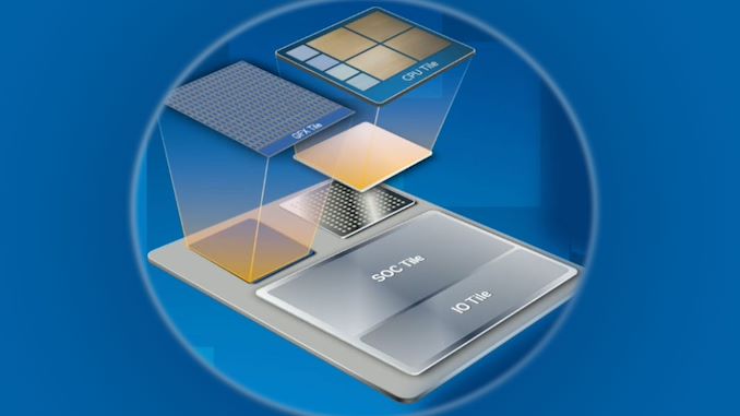
According to Intel, the company is on track to launch Meteor Lake in the second half of the year. And more specifically, at this point Meteor Lake is now in production and ramping alongside the new Intel 4 process.
“CCG's Meteor Lake product on Intel 4 is ramping production wafer starts for an expected launch in the second half of 2023.”
The basis of what we expect will be sold as Intel’s 14th generation of Core processors, Meteor Lake is a critical part for Intel that represents several firsts for the company. It’ll be the first client CPU using chiplets, but also the first heterogenous chiplet CPU from the company, using different chiplets for I/O, CPU cores, graphics, and more. And on the manufacturing side of matters, it’s going to be the lead product for Intel’s next-generation EUV-based Intel 4 process node, as well as Intel’s biggest use of Foveros 3D die stacking technology yet – and the first attempt to do so for a relatively cheap, mass-market processor.
Intel’s last significant update on Meteor Lake came almost exactly a year ago, when the company announced during their Q1’2022 earnings report that it had been successfully powered on for testing. So at a year later, Intel is now making final preparations for a product launch later this year. The official launch window is still in the second half of the year – Intel client processor ramp-ups take several months even without all-new manufacturing technologies in play – so we expect Intel will announce more concrete details on that launch some time in the third quarter.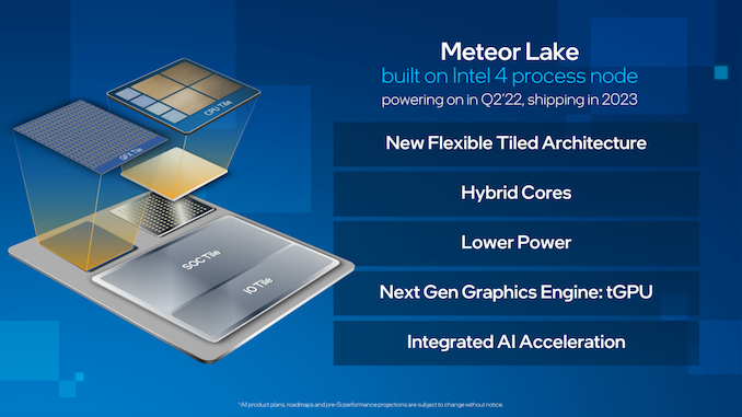
More...
-
04-27-23, 05:05 PM #11710
Anandtech: AMD Issues Second Statement on Ryzen 7000 Burnout Issues: Caps SoC Voltage
Yesterday, AMD issued a statement surrounding the burnout issues some users have been experiencing with their Ryzen 7000X3D processors. The problem, reported in multiple Reddit subforums, includes some Ryzen 7000X3D CPUs burning out part of the chip, and damaging the AM5 socket in the process. This morning, AMD has released a second statement regarding the issue, including what it is doing to rectify the problem and put Ryzen 7000 processor owners at ease.
The official statement from AMD is as follows:
"We have root caused the issue and have already distributed a new AGESA that puts measures in place on certain power rails on AM5 motherboards to prevent the CPU from operating beyond its specification limits, including a cap on SOC voltage at 1.3V. None of these changes affect the ability of our Ryzen 7000 Series processors to overclock memory using EXPO or XMP kits or boost performance using PBO technology.We expect all of our ODM partners to release new BIOS for their AM5 boards over the next few days. We recommend all users to check their motherboard manufacturers website and update their BIOS to ensure their system has the most up to date software for their processor.
Anyone whose CPU may have been impacted by this issue should contact AMD customer support. Our customer service team is aware of the situation and prioritizing these cases."
To counteract the problem, AMD has apparently identified an issue with specific chip voltages going too high when users enable AMD's EXPO memory profiles. A new cap on SoC voltages looks to be the primary change in the AGESA firmware rollout.
However, AMD's broad statement mentions that the update will address multiple power rails, which implies to some degree that the issue may be more than just the SoC power rail – or at least, that AMD isn't taking any chances. So what this entirely means is still a bit up in the air, as AMD hasn't specified in detail what it's doing outside of SoC power limits to prevent Ryzen CPUs from exceeding their specification limits.
Technically speaking, enabling EXPO memory profiles is a form of overclocking – i.e. operating the processor outside of specifications – as AMD's Ryzen 7000 family only officially supports DDR5 memory up to DDR5-5200 speeds. So going past this is putting additional stress on the memory controller in terms of clockspeeds; but the greater concern is how the various voltages on the chip are being adjusted to keep up with the demands of higher memory speeds.
One interesting point about AMD's statement is that it doesn't allude to whether or not the issue is just on its Ryzen 7000X3D processors, or whether it affects all of its Ryzen 7000 processors entirely. Regardless of the Zen 4 chip that users may have, AMD is ambiguous in its language, and it seems to be that AMD is recommended that all users with a Ryzen 7000 series processor should update to the latest firmware.
In practice, enabling EXPO memory profiles on compatible DRAM does seem to push SoC voltages beyond AMD's safe spot on the Ryzen 7000 processors, which AMD is treating as part of the cause of the burnout issue. AMD does, however, state that the changes it has made to their AGESA firmware, once flashed, shouldn't affect the user's ability to apply EXPO memory profiles on compatible kits of DDR5 memory. Which does raise the question of why motherboards were increasing SoC voltages in the first place, as presumably this shouldn't be needed if AMD's new caps won't limit EXPO memory overclocking.
In any case, AMD is actively working with its motherboard partners to release a new AGESA firmware with the new voltage limits, which they say has already been distributed. AMD claims that all AM5 motherboard vendors and models should have a new BIOS version available to them within the next few days, and is recommending all users to update their BIOS at their earliest convenience.
Image source: Speedrookie/Reddit
More...


 Quote
Quote
Thread Information
Users Browsing this Thread
There are currently 22 users browsing this thread. (0 members and 22 guests)


Bookmarks