

Results 11,731 to 11,740 of 12094
Thread: Anandtech News
-
05-18-23, 07:03 PM #11731
Anandtech: Samsung Kicks Off DDR5 DRAM Production on 12nm Process Tech, DDR5-7200 in
Samsung on Thursday said it had started high volume production DRAM chips on its latest 12nm fabrication process. The new manufacturing node has allowed Samsung to reduce the power consumption of its DRAM devices, as well as decrease their costs significantly compared to its previous-generation node.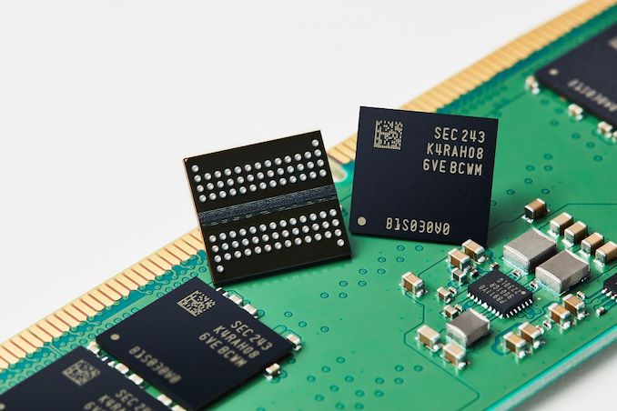
According to Samsung's announcement, the company's 12nm fabrication process is being used to produce 16Gbit DDR5 memory chips. And while the company is already producing DDR5 chips with that capacity (e.g. K4RAH086VB-BCQK), the switch to the newer and smaller 12nm process has paid off both in terms of power consumption and die size. As compared to DDR5 dies made on the company's previous-generation node (14nm), the new 12nm dies offer up to 23% lower power consumption, and Samsung is able to produce 20% more dies per wafer (i.e., the DDR5 dies are tangibly smaller).
Samsung says that the key innovation of its 12nm DRAM fabrication process is usage of new high-k material for DRAM cell capacitors that enabled it to increase cell's capacitance to boost performance, but without increasing their dimensions and die sizes. Higher DRAM cell capacitance means a DRAM cell can store more data and reduce power-draining refresh cycles, hence increasing performance. However, larger capacitors typically result in increased cell and die size, which makes the resulting dies more expensive.
DRAM makers have been addressing this by using high-k materials for years, but finding these materials is getting trickier with each new node as memory makers also have to take into account yields and production infrastructure they have. Apparently, Samsung has succeeded in doing so with its 12nm node, though it does not make any disclosures on the matter. That Samsung has succeeded in reducing their die size by a meaningful amount at all is quite remarkable, as analog components like capacitors were some of the first parts of chips to stop scaling down further with finer process nodes.
In addition to introducing a new high-k material, Samsung also reduced operating voltage and noise for its 12nm DDR5 ICs to offer a better balance of performance and power consumption compared to predecessors.
One of the aspects about Samsung's 12nm DRAM technology is that it looks to be the company's 3rd Generation production node for memory that uses extreme ultraviolet lithography. The first D1x node was purely designed as a proof of concept and its successor D1a, which has been in use since 2021, used EUV for five layers. Meanwhile, it is unclear to what degree Samsung's 12nm node is using EUV tools.
"Using differentiated process technology, Samsung’s industry-leading 12nm-class DDR5 DRAM delivers outstanding performance and power efficiency," said Jooyoung Lee, Executive Vice President of DRAM Product & Technology at Samsung Electronics.
Meanwhile, Samsung is also eyeing faster memory speeds with their new 12nm DDR5 dies. According to the company, these dies can run as fast as DDR5-7200 (i.e. 7.2Gbps/pin), which is well ahead of what the official JEDEC specification currently allows for. The voltage required isn't being stated, but if nothing else, it offers some promise for future XMP/EXPO memory kits.
More...
-
05-20-23, 06:03 AM #11732
Anandtech: Micron to Bring EUV to Japan: 1? Process DRAM to Be Made in Hiroshima in 2
Micron this week officially said that it would equip its fab in Hiroshima, Japan, to produce DRAM chips on its 1γ (1-gamma) process technology, its first node to use extreme ultraviolet lithography, in 2025. The company will be the first chipmaker to use EUV for volume production in Japan and its fabs in Hiroshima and Taiwan will be its first sites to use the upcoming 1γ technology.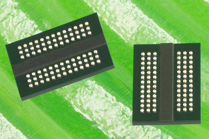
As the only major DRAM maker that has not adopted extreme ultraviolet lithography, Micron planned to start using it with its 1γ process (its 3rd Generation 10nm-class node) in 2024. But due to PC market slump and its spending cuts, the company had to delay the plan to 2025. Micron's 1γ process technology is set to use EUV for several layers, though it does not disclose how many layers will use it.
What the company does say is that its 1γ node will enable the world's smallest memory cell, which is bold claim considering the fact that Micron cannot possibly know what its rivals are going to have in 2025.
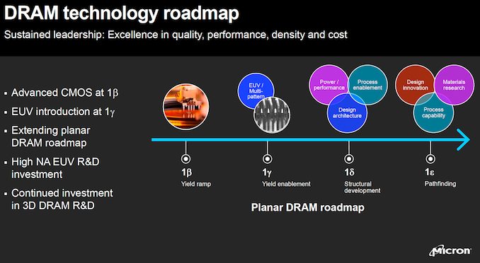
Last year the 1-gamma technology was at the 'yield enablement' stage, which means that the company was testing samples of DRAMs extensive testing and quality control procedures. At this point, the company may implement innovative inspection to tools to identify defects and then introduce certain improvements to certain process steps (e.g., lithography, etching) to maximize yields.
“Micron’s Hiroshima operations have been central to the development and production of several industry-leading technologies for memory over the past decade,” Micron President and CEO Sanjay Mehrotra said. “We are proud to be the first to use EUV in Japan and to be developing and manufacturing 1-gamma at our Hiroshima fab.
To produce memory chips on its 1-gamma node at its Hiroshima fab, Micron needs to install ASML's Twinscan NXE scanners, which cost about $200 million per unit. To equip its fab with advanced tools, Micron secured ¥46.5 billion ($320 million) grant from the Japanese government last September. Meanwhile, Micron says it will invest ¥500 billion ($3.618 billion) in the technology 'over the next few years, with close support from the Japanese government.'
“Micron is the only company that manufactures DRAM in Japan and is critical to setting the pace for not only the global DRAM industry but our developing semiconductor ecosystem,” said Satoshi Nohara, METI Director-General of the Commerce and Information Policy Bureau. “We are pleased to see our collaboration with Micron take root in Hiroshima with state-of-the-art EUV to be introduced on Japanese soil. This will not only deepen and advance the talent and infrastructure of our semiconductor ecosystem, it will also unlock exponential growth and opportunity for our digital economy.”
More...
-
05-23-23, 12:39 AM #11733
Anandtech: Intel HPC Updates For ISC 2023: Aurora Nearly Done, More Falcon Shores, an
With the annual ISC High Performance supercomputing conference kicking off this week, Intel is one of several vendors making announcements timed with the show. As the crown jewels of the company’s HPC product portfolio have launched in the last several months, the company doesn’t have any major new silicon announcements to make alongside this year’s show – and unfortunately Aurora isn’t yet up and running to take a shot at the Top 500 list. So, following a tumultuous year thus far that has seen significant shifts in Intel’s GPU roadmap in particular, the company is using ISC to recompose itself and use the backdrop of the show to lay out a fresh roadmap for HPC customers.
Most notably, Intel is using this opportunity to better explain some of the hardware development decisions the company has made this year. That includes Intel’s pivot on Falcon Shores, transforming it from XPU into a pure GPU design, as well to a few more high-level details of what will eventually become Intel’s next HPC-class GPU. Although Intel would clearly be perfectly happy to keep selling CPUs, the company has (and continues to) realign for a diversified market where their high-performance customers need more than just CPUs.
More...
-
05-23-23, 12:39 AM #11734
Anandtech: Kioxia BG6 Series M.2 2230 PCIe 4.0 SSD Lineup Adds BiCS6 to the Mix
Kioxia's BG series of M.2 2230 client NVMe SSDs has proved popular among OEMs and commercial system builders due to their low cost and small physical footprint. Today, the company is introducing a new generation of products in this postage stamp-sized lineup. The BG6 series builds up on the Gen 4 support added in the BG5 by updating the NAND generation from BiCS5 (112L) to BiCS6 (162L) for select capacities. The increase in per-die capacity now allows Kioxia to bring 2TB M.2 2230 SSDs into the market. While the BG5 series came in capacities of up to 1TB, the BG6 series adds a 2TB SKU. However, the NAND generation update is only reserved for the 1TB and 2TB models.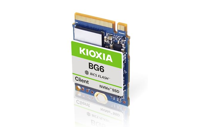
The BG series of SSDs from Kioxia originally started out as a single-chip solution for OEMs either in a BGA package or a M.2 2230 module. The appearance of PCIe 4.0 and its demands for increased thermal headroom resulted in Kioxia getting rid of the single-chip BGA solution starting with the BG5 introduced in late 2021. The BG6 series continues the DRAMless strategy and dual-chip design (separate controller and flash packages) of the BG5.
While the performance numbers for the BG5 strictly placed it in the entry-level category for PCIe 4.0 SSDs, the update to the NAND has now amplified the performance to accepted mainstream levels for this segment. The DRAMless nature and use of the system DRAM (host memory buffer - HMB) for storing the flash translation layer (FTL) handicaps the performance slightly, preventing it from reaching high-end specifications. However, this translates to lower upfront cost and better thermal performance / lowered cooling costs - which are key constraints for OEMs and pre-built system integrators.
The company is focusing on the 1TB and 2TB SKUs with BG6 due to higher demand for those capacities in the end market. The 256GB and 512GB variants are under development. While the M.2 2230 form-factor is expected to be the mainstay, Kioxia is also planning to sell single-sided M.2 2280 versions for systems that do not support M.2 2230 SSDs.Kioxia BG6 SSD Specifications Capacity 256 GB 512 GB 1 TB 2 TB Form Factor M.2 2230 or M.2 2280 Interface PCIe Gen4 x4, NVMe 1.4c NAND Flash 112L BiCS5 3D TLC 162L BiCS6 3D TLC Sequential Read ? MB/s ? MB/s 6000 MB/s 6000 MB/s Sequential Write ? MB/s ? MB/s 5000 MB/s 5300 MB/s Random Read ? IOPS ? IOPS 650K IOPS 850K IOPS Random Write ? IOPS ? IOPS 900K IOPS 900K IOPS Power Active ? W ? W ? W ? W Idle ? mW ? mW ? mW ? mW
In addition to client systems, Kioxia also expects the BG6 SSDs to be used as boot drives in servers and storage arrays. Towards this, a few features that are not considered essential for consumer SSDs (such as support for NVMe 1.4c specifications including interfacing over SMBus for tigher thermal management, encryption using TCG Pyrite / Opal, power loss notification for protection against forced shutdowns, and platform firmware recovery) are included.
The availability of performance numbers for the 1TB SKU allows us to note that the BG6 has more than 1.7x the sequential performance numbers of the BG5, and random reads are 1.3x better, while random write performance has doubled. These are obviously fresh out-of-the-box numbers (as typical of specifications for consumer / client SSDs). Power consumption numbers were not made available at the time of announcement [Update: Kioxia indicated that the finalized specifications (inclusive of power numbers) should become available in July].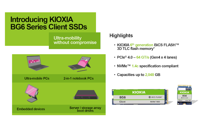
Kioxia will be sampling the drives to OEMs and system integrators in the second half of the year. Systems equipped with these drives can be expected in the hands of consumers for the holiday season or early next year. Pricing information was not provided as part of the announcement, but Kioxia is demonstrating these at the Dell Technologies World 2023 being held in Las Vegas from May 22 - 25.
More...
-
05-23-23, 12:12 PM #11735
Anandtech: AMD Launches Zen 2-based Ryzen and Athlon 7020C Series For Chromebooks
Last year, AMD unveiled their entry-level 'Mendicino' mobile parts to the market, which combine their 2019 Zen 2 cores and their RDNA 2.0 integrated graphics to create an affordable selection of configurations for mainstream mobile devices. Although much of the discussion over the last few months has been about their Ryzen 7040 mobile parts, AMD has launched four new SKUs explicitly designed for the Chromebook space, the Ryzen and Athlon 7020C series.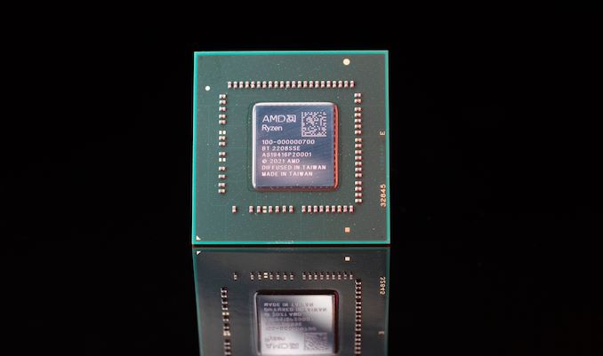
Some of the most notable features of AMD's Ryzen/Athlon 7020C series processors for Chromebooks include three different configurations of cores and threads, ranging from entry-level 2C/2T up to 4C/8T, all with AMD's RDNA 2-based Radeon 610M mobile integrated graphics. Designed for a wide variety of tasks and users, including and not limited to consumers, education, and businesses, AMD's Ryzen 7020C series looks to offer similar specifications and features to their regular 7020 series mobile parts but expands things to the broader Chromebook and ChromeOS ecosystem too.
More...
-
05-23-23, 12:12 PM #11736
Anandtech: Micron Expects Impact as China Bans Its Products from 'Critical' Industrie
In the latest move in the tit-for-tat technology trade war between the United States and China, on Sunday the Cyberspace Administration of China announced that it was effectively banning Micron's products from being purchased in the country going forward. Citing that Micron's products have failed to pass its cybersecurity review requirements, the administration has ordered that operators of key infrastructure should stop buying products containing chips from the U.S.-based company.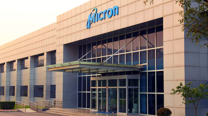
"The review found that Meiguang's products have serious hidden dangers of network security problems, which cause major security risks to China's key information infrastructure supply chain and affect China's national security," a statement by CAC reads. "Therefore, the Cyber Security Review Office has made a conclusion that it will not pass the network security review in accordance with the law. According to the Cyber Security Law and other laws and regulations, operators of key information infrastructure in China should stop purchasing Micron's products."
The CAC statement does not elaborate on the nature of 'hidden dangers' and about the risks they pose. Furthermore, the agency did not detail which companies are considered as 'operators of key information infrastructure,' though we can speculate that these are telecommunication companies, government agencies, cloud datacenters serving socially important clients, and a variety of other entities that may deem crucial for the society or industries.
For U.S.-based Micron, while the Chinese market is a minor one overall, it's not so small to be inconsequential. China and Hong Kong represent some 25% of Micron's revenues, so the drop in sales is expected to have an impact on Micron's financials.
"As we have disclosed in our filings, China and Hong Kong headquartered companies represent about 16% of our revenues," said Mark Murphy, Chief Financial Officer at Micron, at the 51st Annual J.P. Morgan Global Technology, Media and Communications Conference. "In addition, we have distributors that sell to China headquartered companies. We estimate that the combined direct sales and indirect sales through distributors to China headquartered companies is about a quarter of our total revenue."
The trade war implications aside, the 'key information infrastructure' wording of the government order leaves unclear for now on just how wide the Micron ban will be. Particularly, whether Micron's products will still be allowed to be imported for rank-and-file consumer goods. Many of Micron's Chinese clients assemble PCs, smartphones, and other consumer electronics sold all around the world, so the potential the impact on Micron's sales could be significantly lower than 25% of its revenue so long as they are allowed to continue using Micron's parts.
"We are evaluating what portion of our sales could be impacted by a critical information infrastructure ban," Murphy added. "We are currently estimating a range of impact in the low single digits percent of our company total revenue at the low end and high single-digit percentage of total company revenue at the high end."
The decision CAC decision comes after the U.S. government barred Chinese chipmakers from buying advanced wafer fab equipment, which is going to have a significant impact on China-based SMIC and YMTC, and years after the U.S. government implemented curbs that essentially drove one of China's emerging DRAM makers out of business. Officially, whether or not the CAC decision has been influenced by the sanctions against Chinese companies by the U.S. government is an unanswered question, but as the latest barb between the two countries amidst their ongoing trade war, it's certainly not unprecedented.
Sources: Micron, Reuters, SeekingAlpha, CAC.
More...
-
05-25-23, 03:17 AM #11737
Anandtech: Corsair Launches 2000D Airflow SFF Cases For Triple-Slot GPUs
Corsair has expanded the brand's mini-ITX case lineup with the new 2000D Airflow series. The 2000D Airflow and 2000D RGB Airflow small-form-factor (SFF) cases cater specifically to compact but high-performance systems. With a volume of 24.4 liters, the Corsair 2000D series cases have enough landscape to house the most demanding hardware, including a 360 mm AIO CPU liquid cooler and full-size graphics cards up to a triple-slot design.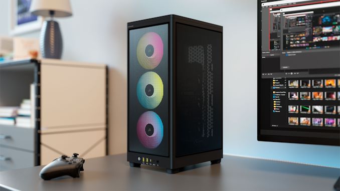
The 2000D Airflow is available with and without RGB-lit fans and in white or black colors. Therefore, the case comes in four different variants. Regardless, the 2000D Airflow is a mini-ITX case that prioritizes airflow for the components housed inside. For this same reason, Corsair designs the 2000D Airflow with removable steel mesh front, side, and rear panels for maximum ventilation from all directions. The case measures 18.03 x 10.67 x 7.87 inches and weighs just under 10 pounds. As a result, it doesn't require much space whether users decide to put it on or under the desk. Being an SFF case, the 2000D Airflow only accepts mini-ITX motherboards.
The 2000D Airflow can accommodate up to eight 120 mm and two 140 mm cooling fans, doing the case's name justice. If a user fits the 2000D Airflow with a single-slot graphics card, it opens the possibility of cooling the graphics card with two additional fan mounts. For CPU air cooling enthusiasts, the 2000D Airflow supports coolers with a maximum height of up to 6.69 inches. Given the generous amount of fan mounts, Corsair's SFF case offers plentiful liquid cooling options. It supports 120 mm, 140 mm, 240 mm, 280 mm, and 360 mm radiators. Users can fit up to multiple radiators with an example combination of a 360 mm unit on the side and a 240 mm one at the rear in a scenario with a single-slot graphics card.
Gallery: Corsair 2000D Airflow


The 2000D Airflow has three case expansion slots, accommodating beefy graphics cards with up to three PCI slots in a vertical orientation. Consumers will have no problem fitting a GeForce RTX 4090 into the 2000D Airflow. However, they must ensure the graphics card is shorter than 14.37 inches since that's the maximum length permitted inside the 2000D Airflow.
Storage options, however, are limited to three 2.5-inch drives, whether SSDs or hard drives, with the 2000D Airflow. In addition, one of the case's caveats is that it only accepts SFX or SFL-L power supplies, reducing options to units with a length of up to 5.12 inches. Nevertheless, Corsair aficionados will have no issues finding an adequate unit within the brand's ecosystem since the company offers the SF series and SF-L series with capacities varying from 600 watts to 750 watts on the former and 850 watts to 1,000 watts on the latter. Regarding the I/O design, the 2000D Airflow offers one USB 3.2 Gen 2 Type-C port, two USB 3.2 Gen 1 Type-A ports, and one 3.5 mm audio jack on the front panel.
The 2000D Airflow retails for $139.99. On the other hand, the 2000D RGB Airflow, which has three pre-installed Corsair AF120 RGB Slim fans in the front intake, will set consumers back $199.99. Corsair backs its 2000D Airflow cases with a two-year warranty. In the case of the RGB variant, the AF120 RGB Slim fans come with a three-year warranty.
More...
-
05-26-23, 04:15 AM #11738
Anandtech: NVIDIA Reports Q1 FY2024 Earnings: Bigger Things to Come as NV Approaches
Closing out the most recent earnings season for the PC industry is, as always, NVIDIA. The company’s unusual, nearly year-ahead fiscal calendar means that they get the benefit of being casually late in reporting their results. And in this case, they’ve ended up being the proverbial case of saving the best for last.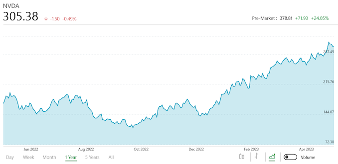
For the first quarter of their 2024 fiscal year, NVIDIA booked $7.2 billion in revenue, which is a 13% drop over the year-ago quarter. Like the rest of the chip industry, NVIDIA has been weathering a significant slump in demand for computing products over the past few quarters, which in turn has dented NVIDIA’s revenue and profitability. However, while NVIDIA’s consumer-focused gaming division has continued to take matters on the chin, the strong performance of NVIDIA’s data center group has kept the company as a whole fairly profitable, with the most recent quarter setting a segment record and helping NVIDIA to avoid the tough financial situations faced by rivals AMD and Intel.
To that end, while Q1’FY24 was not by any means a record quarter for NVIDIA, it was still a relatively strong one for the company. NVIDIA’s net income of $2 billion makes for one of their better quarters in that regard, and it’s actually up 26% year-over-year despite the revenue drop. That said, reading between the lines will find that NVIDIA paid their Arm acquisition breakup fee last year (Q1’FY23), so NVIDIA’s GAAP net income looks a bit better than it otherwise would; while non-GAAP net income would be down 21%. Meanwhile, NVIDIA’s gross margins have held strong in the most recent quarter, with NVIDIA posting a GAAP gross margin of 64.6%.NVIDIA Q1 FY2024 Financial Results (GAAP) Q1 FY2024 Q4 FY2023 Q1 FY2023 Q/Q Y/Y Revenue $7.2B $6.1B $8.3B +19% -13% Gross Margin 64.6% 63.3% 65.5% +1.3ppt -0.9ppt Operating Income $2.1B $1.3B $1.9B +70% +15% Net Income $2.0B $1.4B $1.6B +44% +26% EPS $0.82 $0.57 $0.64 +44% +28%
But even a solid quarter during an industry slump is arguably not the biggest news to come out of NVIDIA’s most recent earnings report. Rather, it’s the company’s projections for Q2’FY24. In short, NVIDIA is expecting revenue to explode in Q2, with the company forecasting $11 billion in sales. Should it come to fruition, such a quarter would blow well past NVIDIA’s previous revenue records – and shattering Wall Street expectations. As a result, NVIDIA’s stock has already taken off in overnight trading, and by the time the market opens a bit later this morning, NVIDIA is expected to be a $930B+ company, knocking on the door of crossing a market capitalization of a trillion dollars.
More...
-
05-26-23, 04:15 AM #11739
Anandtech: TSMC: We Have Working CFET Transistors in the Lab, But They Are Generation
Offering an update on its work with complementary field-effect transistors (CFETs) as part of the company's European Technology Symposium 2023, TSMC has revealed that it has working CFETs within its labs. But even with the progress TSMC has made so far, the technology is still in its early days, generations away from mass production. In the meantime, ahead of CFETs will come gate-all-around (GAA) transistors, which TSMC will be introducing with its TSMC's upcoming N2 (2nm-class) production nodes.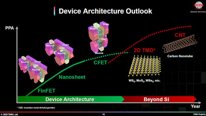
One of TSMC's long-term bets as the eventual successor to GAAFETs, CFETs are expected to offer advantages over GAAFETs and FinFETs when it comes to power efficiency, performance, and transistor density. However, these potential benefits are theoretical and dependent on overcoming significant technical challenges in fabrication and design. In particular, CFETs are projected to require the usage of extremely precise lithography (think High NA EUV tools) to integrate both n-type and p-type FETs into a single device, as well as determining the most ideal materials to ensure appropriate electronic properties.
Just like other chip fabs, TSMC is working on a variety of transistor design types, so having CFETs working in the lab is important. But it's also not something that is completely unexpected; researchers elsewhere have previously assembled CFETs, so now it's up to industry-focused TSMC to figure out how to bring about mass production. To that end, TSMC is stressing that CFETs are not in the near future.
"Let me make a clarification on that roadmap, everything beyond the nanosheet is something we will put on our [roadmap] to tell you there is still future out there," said Kevin Zhang, senior vice president at responsible for technology roadmap, business strategy. "We will continue to work on different options. I also have the add on to the one-dimensional material-[based transistors] […], all of those are being researched on being investigated on the future potential candidates right now, we will not tell you exactly the transistor architecture will be beyond the nanosheet."
Indeed, research projects take a long time and when you are running many of them in parallel, you never know which of them comes to fruition. Even at that point, it is hard to tell which of potential structure candidates TSMC (or any other fabs) will choose, Ultimately, fabs have to meet the needs of their larger customers (e.g., Apple, AMD, MediaTek, Nvidia, Qualcomm) at the time when this production node is ready for high volume manufacturing.
To that end, TSMC is going to use GAA structures for years to come, according to Zhang.
"Nanosheet is starting at 2nm, it is reasonable to project and that nanosheet will be used for at least a couple of generations, right," asked Zhang rhetorically. "So, if you think about CFETs, we've leveraged [FinFETs] for five generations, which is more than 10 years. Maybe [device structure] is somebody else's problem to worry, then you can continue to write a story."
Source; TSMC European Technology Symposium 2023
More...
-
05-26-23, 11:19 PM #11740
Anandtech: TSMC Preps 6x Reticle Size Super Carrier Interposer for Extreme SiP Proces
As part of their efforts to push the boundaries on the largest manufacturable chip sizes, Taiwan Semiconductor Manufacturing Co. is working on its new Chip-On-Wafer-On-Substrate-L (CoWoS-L) packaging technology that will allow it to build larger Super Carrier interposers. Aimed at the 2025 time span, the next generation of TSMC's CoWoS technology will allow for interposers reaching up to six times TSMC's maximum reticle size, up from 3.3x for their current interposers. Such formidable system-in-packages (SiP) are intended for use by performance-hungry data center and HPC chips, a niche market that has proven willing to pay significant premiums to be able to place multiple high performance chiplets on a single package.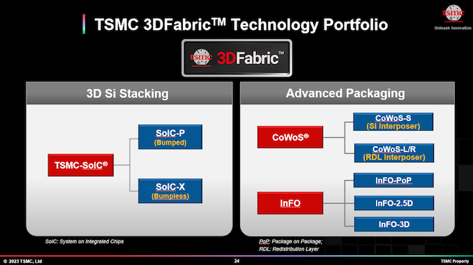
"We are currently developing a 6x reticle size CoWoS-L technology with Super Carrier interposer technology," said said Yujun Li, TSMC's director of business development who is in charge of the foundry's High Performance Computing Business Division, at the company's European Technology Symposium 2023.
Global megatrends like artificial intelligence (AI) and high-performance computing (HPC) have created demand for seemingly infinite amounts of compute horsepower, which is why companies like AMD, Intel, and NVIDIA are building extremely complex processors to address those AI and HPC applications. One of the ways to increase compute capabilities of processors is to increase their transistor count; and to do so efficiently these days, companies use multi-tile chiplet designs. Intel's impressive, 47 tile Ponte Vecchio GPU is a good example of such designs; but TSMC's CoWoS-L packaging technology will enable the foundry to build Super Carrier interposers for even more gargantuan processors.
The theoretical EUV reticle limit is 858mm2 (26 mm by 33 mm), so six of these masks would enable SiPs of 5148 mm2. Such a large interposer would not only afford room for multiple large compute chiplets, but it also leaves plenty of room for things like 12 stacks of HBM3 (or HBM4) memory, which means a 12288-bit memory interface with bandwidth reaching as high as 9.8 TB/s.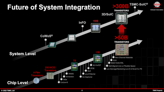
"The Super Carrier interposer features multiple RDL layers on the front as well as on the backside of the interposer for yield and manufacturability," explained Li. "We can also integrate various passive components in the interpreter for performance. This six reticle-size CoWoS-L will be qualified in 2025"
Building 5148 mm2 SiPs is an extremely tough tasks and we can only wonder how much they will cost and how much their developers will charge for them. At present NVIDIA's H100 accelerator, whose packaging spans an interposer multiple reticles in size, costs around $30,000. So a considerable larger and more powerful chip would likely push prices higher still.
But paying for the cost of large processors will not be the only huge investments that data center operators will need to make. The amount of active silicon that 5148 mm2 SiPs can house will almost certainly result in some of the most power-hungry HPC chips produced yet – chips that will also need equally powerful liquid cooling to match. To that end, TSMC has disclosed that it has been testing on-chip liquid cooling technology, stating that it has managed to cool down silicon packages with power levels as high as 2.6 kW. So TSMC does have some ideas in mind to handle the cooling need of these extreme chips, if only at the price of integrating even more cutting-edge technology.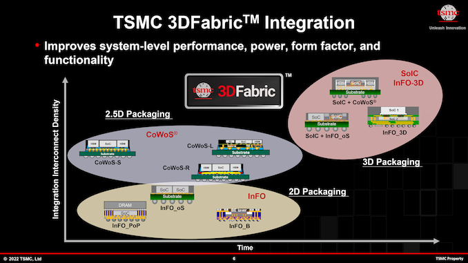
More...


 Quote
QuoteThread Information
Users Browsing this Thread
There are currently 19 users browsing this thread. (0 members and 19 guests)


Bookmarks