

Results 11,771 to 11,780 of 12091
Thread: Anandtech News
-
06-21-23, 01:01 PM #11771
Anandtech: Micron Unveils First UFS 4.0 Modules: Up to 4,300 MB/s Storage for Smartph
Micron on Wednesday introduced its first UFS 4.0-compliant storage devices. The company's latest generation of single-module smartphone storage devices are slated to be the fastest yet, offering a combination of improvements coming from the UFS specification itself, along with including newer, faster NAND within the storage devices. Micron expects its UFS 4 devices to be used by upcoming flagship smartphones, tablets, and ultra-low-power notebooks already this year.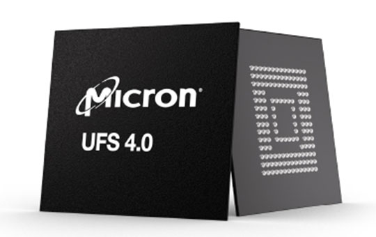
Micron's UFS 4.0 storage devices come in three capacities — 256 GB, 512 GB, and 1 TB — that rely on the company's own controller. The higher-end 512 GB and 1 TB UFS 4.0 products use Micron's 232-layer six-plane 1 Tb 3D TLC NAND devices and can provide sequential read speed of up to 4,300 MB/s as well as sequential write speed of up to 4,000 MB/s, which makes them the highest performing UFS storage modules for smartphones to date, based on data supplied by Micron. The 256 GB unit is slightly slower as it uses quad-plane 3D NAND devices.
The new UFS 4.0 storage modules from Micron are fully compliant with the specification and use two M-PHY Gear 5 lanes for data transmission. In addition, they support such proprietary firmware capabilities as Data Stream Separation (separates frequently used and rarely data on the device to reduce background garbage collection), Auto Read Burst (improves read performance by using device de-fragmentation after it is used for a long time), and Eye Monitoring (ensures signal integrity).
In addition to offering higher performance than predecessors, Micron's UFS 4.0 modules are said to feature a 25% higher energy efficiency achieved through a combination of higher performance and energy saving capabilities.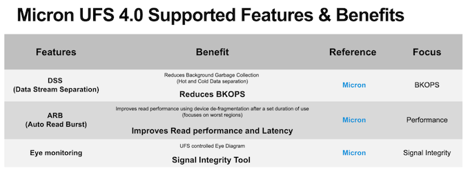
“Micron’s latest mobile solution tightly weaves together our best-in-class UFS 4.0 technology, proprietary low-power controller, 232-layer NAND and highly configurable firmware architecture to deliver unmatched performance,” said Mark Montierth, corporate vice president and general manager of Micron’s Mobile Business Unit.
Usage of high-capacity 232-layer 3D TLC NAND devices also enables Micron to make its UFS 4.0 modules rather thin. The company says that their z-height does not exceed 0.8 – 0.9 mm, which will enable makers of handsets to either make their products slimmer, or fit in a higher-capacity battery.
Micron is currently sampling its UFS 4.0 storage modules with leading smartphone makers and expects these units to be used in the coming months or quarters after it starts mass production in the second half of the year.
More...
-
06-21-23, 01:01 PM #11772
Anandtech: Intel to Spend Tens of Billions on New Fabs in Germany and Israel
Intel is spending tens of billions of dollars on new fabs in Arizona and Oregon, but the company's ambitions certainly do not end in the U.S. This month the company revealed its finalized plans for new production capacities in Europe and Middle East with intentions to invest over $50 billion.
Intel's new 'Silicon Junction' site near Magdeburg, Germany, will accommodate at two fabs and will initially cost €30 billion. The manufacturing facilities will make chips on an 'Angstrom-era' node, though Intel does not disclose which one for now. The only thing that the company reveals for now is that the production node will be more advanced than the one Intel envisioned for the fab originally, which can point to nodes that are more advanced than Intel 20A and Intel 18A. The property needed for this upcoming project was purchased by Intel in November 2022. After the European Union greenlights the incentive package, the first fab will be up and running within four to five years, Intel claims.
Intel disclosed original plans for a chip plant near Magdeburg, Germany, in early 2022. Back then, the fab was estimated to cost $18.7 billion, and the German government agreed to provide $7.2 billion in state aid. However, Intel later chose to broaden the project's scope, intending to construct a bigger and more technologically advanced plant with total investments amounting to $31.675 billion (€30 billion). This expansion necessitated additional subsidies, leading to prolonged negotiations between Intel and the German authorities. Finally, a revised agreement was reached this week, granting Intel €10 billion ($10.91 billion) in government aid for the construction of the new fab.
Alongside developing a brand new fab complex in Germany, Intel has plans to extend its site in Kiryat Gat, Israel. The CPU giant is slated to invest some $25 billion into constructing and equipping this new Israeli fab, as reported by Benjamin Netanyahu, Israel's prime minister. This signifies the most substantial foreign investment ever received by Israel.
The new Kiryat Gat facility is set to start production in 2027 and is expected to operate until at least 2035, which, according to the Israeli Finance Ministry, should create thousands of well-paid jobs. Under the terms of this deal, Intel will see its tax rate increase from the present 5% to 7.5%.
Building new fabs in will significantly increase Intel's manufacturing capacities available for its own products and for chips designed by clients of its Intel Foundry Services unit. In addition to advanced chip production facilities in Germany and Ireland, the company will also construct a new advanced packaging facility near Wroclaw, Poland, which will allow Intel to build and package chips entirely in Europe instead of bringing them to Asia for packaging.
This new advanced packaging facility near Wroclaw, Poland, is projected to fulfill the critical need for assembly and testing capacity that Intel foresees by 2027. The company plans to invest up to $4.6 billion into the project, designed to allow for future expansion. Upon completion, it is expected to employ about 2,000 staff members.
Sources: Intel, Intel, Reuters
More...
-
06-22-23, 09:55 AM #11773
Anandtech: Intel Discontinues Arc A770 Limited Edition Graphics Card
In a rather unexpected move, Intel this week discontinued its Arc A770 Limited Edition graphics card, which was its flagship discrete graphics offering for desktops. Intel's partners will continue to offer their Arc A770 add-in-boards (AIBs) with 8 GB and 16 GB of GDDR6 memory.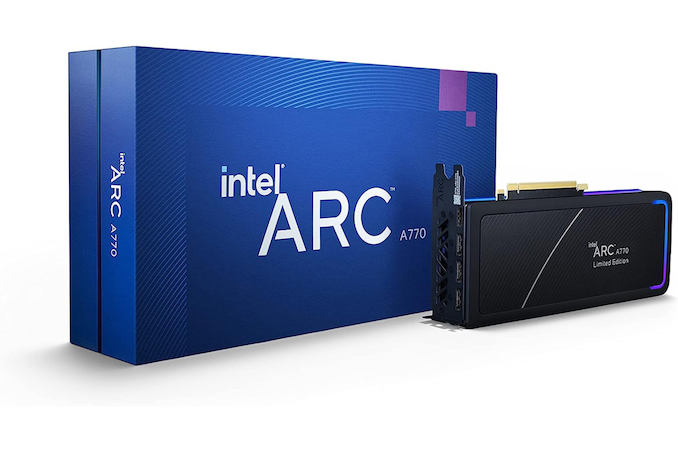
Intel discontinues its Arc A770 Limited Edition graphics card rather abruptly: the company listed June 20, 2023 as the last product order date and the last product shipment date, which essentially means that it no longer produces and ships these boards. As soon as the remaining stock of these products will be depleted in the channel, they will no longer be available. Apparently, the product was a Limited Edition indeed since it is being EOLed less than a year on the market.
A quick check at Amazon and Newegg reveals that the Arc A770 LE board is available for as much as $497.35 at Amazon and is no longer available at Newegg. Meanwhile, Newegg has three CPU + A770 graphics cards bundles containing Acer's Predator BiFrost Arc A770 16 GB AIBs. Separately, this board costs $339 at Newegg.
Intel's own Arc A750 Limited Edition and Arc A770 Limited Edition graphics cards were meant to bring the audience the best experience possible with an all-new GPU family. In addition, they demonstrated that Intel wanted its Arc A700-series products to compete for the mainstream market segment without using fancy and huge cooling systems. Indeed, Intel's own Arc A750 LE and Arc A770 LE boards look very modest, yet provided everything that the company's ACM-G10 GPU had to offer in terms of performance and functionality.
By now, there are Intel Arc A770 graphics cards from numerous AIB producers, including ASRock, Acer, Gigabyte, Gunnir, MSI, and Sparkle, so Intel does not really need to offer its own cards to ensure that its top-of-the-line product is present on the market.
Interestingly, but Intel's Arc A750 Limited Edition graphics cards remains afloat for now. Perhaps, while Intel still has these boards in its own stock.
Source: Intel
More...
-
06-22-23, 09:55 AM #11774
Anandtech: Transcend ESD310C Dual-Interface UFD Review: Silicon Motion Powers Portabl
Transcend recently introduced the ESD310C portable SSD in a thumb drive form-factor. A compact device with both Type-A and Type-C USB 3.2 Gen 2 (10 Gbps) interfaces, the ESD310C is also attractively priced. The product is based on Silicon Motion's SM2320 native USB flash drive controller, and is quite similar to the Kingston DataTraveler Max A in terms of internal components. Read on to find out what the SM2320 can deliver in a slightly different form factor, and how Transcend manages to differentiate the ESD310C from the other 10 Gbps thumb drives in the market.
More...
-
06-23-23, 04:20 AM #11775
Anandtech: Gigabyte's Low-Cost Mini-ITX A620 Motherboard Supports Ryzen R9 7950X, R9
Gigabyte has quietly introduced one of the industry's first inexpensive motherboards for AMD's AM5 processors in Mini-ITX form-factor. The most unexpected peculiarity of Gigabyte's A620I AX motherboard — based on AMD's low-cost A620 chipset that only supports essential features — is that it supports AMD's top-of-the-range Ryzen 9 7950X3D and Ryzen 9 7950X processors.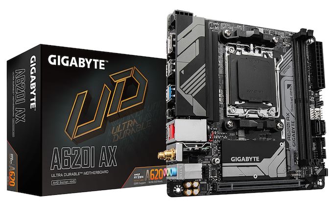
Despite its positioning as an entry-level motherboard for AMD's Ryzen 7000-series CPUs based on the Zen 4 microarchitecture, Gigabyte's Ultra Durable A620I-AX can handle all of AMD's AM5 CPUs released to date, including relatively inexpensive Ryzen 5 7600 with a 65W TDP as well as range-topping Ryzen 9 7950X3D with 3D V-Cache rated for 120W and Ryzen 9 7950X rated for 170W. Given that AMD's A620 platform is not meant for overclocking, the Ryzen 9 7950X cannot be overclocked on this motherboard, but even support of this CPU is unexpected.
AMD's Ryzen 7000-series CPUs are hungry for memory bandwidth and the UD A620I-AX does not disappoint here as it comes with two slots for DDR5 memory that officially support memory modules rated for up to DDR5-6400 and with EXPO profiles. High-performance DDR5 DIMMs will be beneficial not only for Ryzen 9 and Ryzen 7 CPUs aimed at demanding gamers, but will also be beneficial for cheap PCs running AMD's upcoming AM5 APUs with built-in graphics as memory bandwidth is crucial for integrated GPUs. The motherboard even has two display outputs to support iGPUs.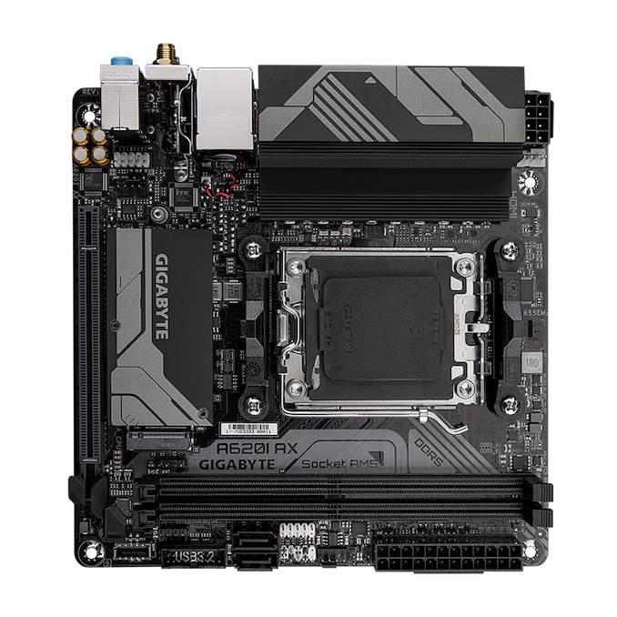
Speaking of gaming, the UD A620I-AX motherboard naturally lacks any kind of PCIe Gen5 support, but it does have a PCIe 4.0 x16 slot for graphics cards and an M.2-2280 slot with a PCIe 4.0 x4 interface for SSDs. For those who need additional storage space, the platform has two SATA ports.
As for overall connectivity, the UD A620I-AX motherboard features a Wi-Fi 6 + Bluetooth adapter, an 2.5GbE port, USB 3.2 Gen1/2 ports (including a Type-C port), and audio connectors. While this may not seem much, entry level gaming systems do not use a lot of high-performance peripherals anyway. Furthermore, AMD's A620 platform does not support USB4.
Pricing details for the UD A620I-AX are not yet available, but some early reports suggest that it will be priced below/around $100, like other A620-based offerings. Meanwhile, given support for high-end Ryzen 9 processors and Mini-ITX form-factor, it is possible that Gigabyte may charge a premium for the UD A620I-AX. Therefore, it remains to be seen how reasonably priced will this motherboard be when it hits the market.
Gallery: Gigabyte's Low-Cost Mini-ITX A620 Motherboard Supports Ryzen R9 7950X, R9 7950X3D CPUs


More...
-
06-23-23, 04:20 AM #11776
Anandtech: The Aurora Supercomputer Is Installed: 2 ExaFLOPS, Tens of Thousands of CP
Argonne National Laboratory and Intel said on Thursday that they had installed all 10,624 blades for the Aurora supercomputer, a machine announced back in 2015 with a particularly bumpy history. The system promises to deliver a peak theoretical compute performance over 2 FP64 ExaFLOPS using its array of tens of thousands of Xeon Max 'Sapphire Rapids' CPUs with on-package HBM2E memory as well as Data Center GPU Max 'Ponte Vecchio' compute GPUs. The system will come online later this year.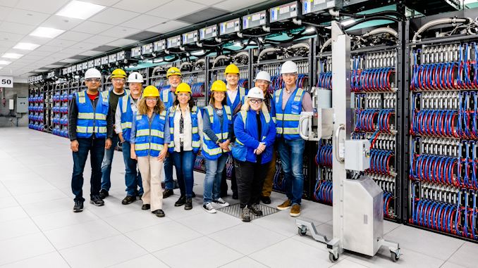
"Aurora is the first deployment of Intel's Max Series GPU, the biggest Xeon Max CPU-based system, and the largest GPU cluster in the world," said Jeff McVeigh, Intel corporate vice president and general manager of the Super Compute Group.
The Aurora supercomputer looks quite impressive, even by the numbers. The machine is powered by 21,248 general-purpose processors with over 1.1 million cores for workloads that require traditional CPU horsepower and 63,744 compute GPUs that will serve AI and HPC workloads. On the memory side of matters, Aurora has 1.36 PB of on-package HBM2E memory and 19.9 PB of DDR5 memory that is used by the CPUs as well as 8.16 PB of HBM2E carried by the Ponte Vecchi compute GPUs.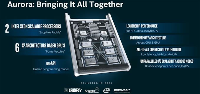
The Aurora machine uses 166 racks that house 66 blades each. It spans eight rows and occupies a space equivalent to two basketball courts. Meanwhile, that does not count the storage subsystem of Aurora, which employs 1,024 all-flash storage nodes offering 220TB of storage capacity and a total bandwidth of 31 TB/s. For now, Argonne National Laboratory does not publish official power consumption numbers for Aurora or its storage subsystem.
The supercomputer, which will be used for a wide variety of workloads from nuclear fusion simulations to whether prediction and from aerodynamics to medical research, uses HPE's Shasta supercomputer architecture with Slingshot interconnects. Meanwhile, before the system passes ANL's acceptance tests, it will be used for large-scale scientific generative AI models.
"While we work toward acceptance testing, we are going to be using Aurora to train some large-scale open-source generative AI models for science," said Rick Stevens, Argonne National Laboratory associate laboratory director. "Aurora, with over 60,000 Intel Max GPUs, a very fast I/O system, and an all-solid-state mass storage system, is the perfect environment to train these models."
Even though Aurora blades have been installed, the supercomputer still has to undergo and pass a series of acceptance tests, a common procedure for supercomputers. Once it successfully clears these and comes online later in the year, it is projected to attain a theoretical performance exceeding 2 ExaFLOPS (two billion billion floating point operations per second). With vast performance, it is expected to secure the top position in the Top500 list.
The installation of the Aurora supercomputer marks several milestones: it is the industry's first supercomputer with performance higher than 2 ExaFLOPS and the first Intel'-based ExaFLOPS-class machine. Finally, it marks the conclusion of the Aurora saga that began eight years ago as the supercomputer's journey has seen its fair share of bumps.
Originally unveiled in 2015, Aurora was initially intended to be powered by Intel's Xeon Phi co-processors and was projected to deliver approximately 180 PetaFLOPS in 2018. However, Intel decided to abandon the Xeon Phi in favor of compute GPUs, resulting in the need to renegotiate the agreement with Argonne National Laboratory to provide an ExaFLOPS system by 2021.
The delivery of the system was further delayed due to complications with compute tile of Ponte Vecchio due to the delay of Intel's 7 nm (now known as Intel 4) production node and the necessity to redesign the tile for TSMC's N5 (5 nm-class) process technology. Intel finally introduced its Data Center GPU Max products late last year and has now shipped over 60,000 of these compute GPUs to ANL.
More...
-
06-26-23, 09:08 PM #11777
Anandtech: SK Hynix Launches Beetle X31 Portable SSD
SK Hynix has introduced the Beetle X31, its first portable SSD. The drive promises to hit sequential transfer rates of up to 1,050 MB/sec when working with appropriate hosts. The drive is ultra compact and can store up to 1 TB of data, which is quite a bit higher than typical USB flash drives.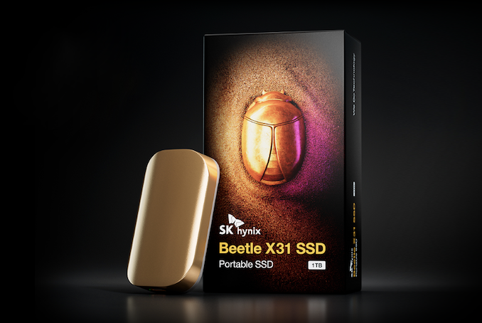
The SK Hynix Beetle X31 uses the company's 128-layer 3D NAND memory and boasts sequential read and write speeds of up to 1,050 MB/sec and 1,000 MB/sec, respectively. Meanwhile, the company promises that the drive can maintain speed of 'over 900 MB/s' though SK Hynix does not disclose the size of its SLC cache.
From performance standpoint, the drive is slower than high-end direct attached storage devices with a Thunderbolt 3 and Thunderbolt 4 interface. Yet, it is reasonable to assume that it will cost significantly less than such DAS devices.
The manufacturer will offer its Beetle X31 in 512 GB and 1 TB versions, which is larger compared to typical inexpensive USB drives.
SK Hynix claims that the Beetle X31 is compatible with PCs, Macs, tablets, game consoles, and Android-based smartphones. The X31 drive features a USB Type-C interface and comes standard with two USB cables (USB C-to-C and C-to-A) and a bumper case.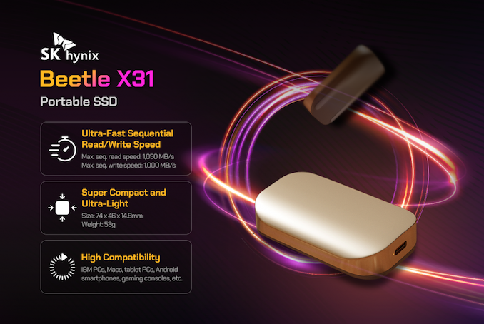
The Beetle X31 measures 74 x 46 x 14.8 mm (which makes it a bit larger compared to USB flash drives) and weighs 53 grams. The drive comes in a sleek aluminum chassis.

"From the onset, the X31 was designed to be incredibly light and ultra-compact," said Chan-dong Park, head of NAND marketing at SK Hynix. "It also shares key component materials with the Gold P31, which features optimal power consumption. So, the X31 was a continuation of the P31’s design with added concepts that are unique to portable SSDs. A lot of effort was spent on enhancing the exterior elements of the product including its color and smooth texture to improve the user experience."
The Beetle X31 is already available in South Korea, it will be released in North America, Europe, and Asia shortly.
More...
-
06-26-23, 09:08 PM #11778
Anandtech: Qualcomm Unveils Snapdragon 4 Gen 2: Modest Modernization For Low-End Mobi
Qualcomm this morning is taking the wraps off its next generation Snapdragon 4-class mobile SoC, the aptly named Snapdragon 4 Gen 2. The company’s new entry-level SoC for smartphones and other devices incorporates some hardware updates that should modestly boost performance for the most cost-sensitive segment of the mobile market, as well as bringing Qualcomm’s overall Snapdragon product stack into closer alignment by supporting more recent 5G standards and fabbing the chip to a newer process node.
First and foremost, the top line on performance is that Qualcomm is touting a 10% boost in CPU performance, thanks to higher CPU core clockspeeds. The Snapdragon 4 Gen 2 uses the same 2+6 CPU core configuration as its predecessor, the Snapdragon 4 Gen 1, with 2 Cortex-A78-derived Kryo CPU cores paired with 6 Cortex-A55-derived cores. Thanks to a node shrink, Qualcomm has boosted the top clockspeeds on each set of cores by about 10%, bringing the A78 cores up to 2.2GHz, and the A55 cores up to 2.0GHz. So the 10% CPU performance gain should be fairly consistent in both single and multi-threaded workloads.
Architecturally, there’s little to say about these cores that hasn’t been said already. These are reasonably performant CPU cores, though the age and the lack of higher clockspeeds means their performance potential is limited. The ultra-budget nature of the Snapdragon 4 series means this will be the last part of Qualcomm’s stack to move to any kind of Armv9 core. Though interestingly, the 4 Gen 2 does get a bit of a leg up over the 6 Gen 1 when it comes to the A55 cores – 6G1’s small cores only boost to 1.8GHz, despite being fabbed on the same process node. So this will narrow the CPU performance gap between those parts a bit (at least until the obligatory 6 Gen 2 lands).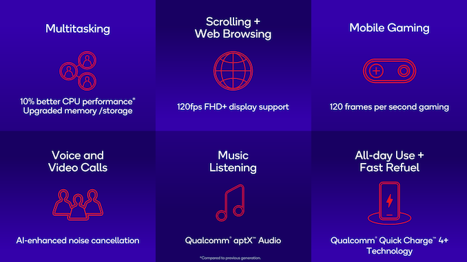
Meanwhile, Qualcomm is staying mum on GPU performance. The company stopped giving their GPUs external product numbers a few years ago, and for the Snapdragon 4 release they are not even issuing performance expectations. So we aren’t expecting any gains here, especially as the chip is still meant to drive HD/FHD devices.
As noted earlier, Qualcomm has moved their entry-level SoC to a Samsung 4nm process (given the timing, 4LPP, we’d assume). That means that Samsung’s entire current product stack – Snapdragons 8G2, 7+G2, 6G1, and 4G2 – are all made on a 4nm node of some flavor. Samsung’s is the less performant of the two, but it’s almost certainly cheaper. Which is a boon for these entry-level, price-constrained parts. Academically, I’m curious just how small the Snapdragon 4 die is based on this process, as it should be rather tiny, but that’s not a detail Qualcomm normally shares.Qualcomm Snapdragon 4-Series SoCs SoC Snapdragon 4 Gen 2
(SM4450)Snapdragon 4 Gen 1
(SM4375)Snapdragon 480
(SM4350)CPU 2x CA78
@ 2.2GHz
6x CA55
@ 2.0GHz2x CA78
@ 2.0GHz
6x CA55
@ 1.8GHz2x CA76
@ 2.0GHz
6x CA55
@ 1.8GHzGPU Adreno Adreno Adreno 619 DSP Hexagon Hexagon Hexagon 686 ISP/
CameraSpectra
(2x 12-bit)
1x 10⁸MP or 32MP with ZSL
or
16+16MP with ZSL
Spectra
(3x 12-bit)
1x 10⁸MP or 32MP with ZSL
or
25+13MP with ZSL
or
3x 13MP with ZSLSpectra 345
(3x 12-bit)
1x 64MP
or
25+13MP
or
3x 13MPEncode/
Decode1080p60
H.264, H.265, VP9 (Decode-Only)Memory 2x 16-bit @ 3200MHz
LPDDR5
25.6GB/s
or
2x 16-bit @ 2133MHz
LPDDR4X
17.0GB/s2x 16-bit @ 2133MHz
LPDDR4X
17.0GB/s2x 16-bit @ 2133MHz
LPDDR4X
17.0GB/sStorage UFS 3.1 (2 lane) UFS 2.2, eMMC 5.1 UFS 2.2, eMMC 5.1 Integrated Modem X61 Integrated
LTE
DL = 800Mbps
UL = 210Mbps
5G NR
Sub-6
(100MHz)
DL = 2500Mbps
UL = 900MbpsX51 Integrated
LTE
DL = 800Mbps
UL = 210Mbps
5G NR
Sub-6 + mmWave
(100MHz)
DL = 2500Mbps
UL = 900MbpsX51 Integrated
LTE
DL = 800Mbps
UL = 210Mbps
5G NR
Sub-6 + mmWave
(100 + 200MHz)
DL = 2500Mbps
UL = 660MbpsWi-Fi/BT Wi-Fi 5 (1x1)
Bluetooth 5.1Wi-Fi 5 (2x2)
Bluetooth 5.2Wi-Fi 5 (2x2)
Bluetooth 5.1Mfc. Process Samsung 4nm TSMC 6nm Samsung 8nm LPP
Otherwise, this latest Snapdragon 4-class SoC is a bit of a give-and-take release as compared to the 4 Gen 1. On the memory side of matters, the new SoC incorporates Qualcomm’s newer controller design, bringing LPDDR5 support to a 4-class chip for the first time. Like other Qualcomm SoCs, the chip can run that memory at up to LPDDR5-6400 speeds. Meanwhile, LPDDR4X remains supported as well, at the usual LPDDR4X-4266 data rate. The memory bus is still a total of 32-bits wide, so you’re looking at a peak memory bandwidth of 25.6GB/second with LPDDR5, a full 50% more bandwidth than what the 4 Gen 1 could provide.
The storage controller has also been updated to support UFS 3.1, finally bringing Qualcomm’s low-end chip up to relatively modern version of the flash storage standard. Compared to the UFS 2.2 spec supported in the previous chip, UFS 3.1 a bit more than doubles the bandwidth per lane; so in a two-lane configuration, the 4G2 can theoretically transfer as much as 2.9GB/second of data though Qualcomm isn’t making any performance claims. Notably, eMMC storage support is absent from Qualcomm’s specification sheet, indicating that support for that now well-outdated interface standard is finally riding off into the sunset.
As for Qualcomm’s imaging ISPs and related hardware, the 4 Gen 2 will be taking a step backwards by removing the third camera pipeline. As a result, 4 Gen 2 will only support up to two cameras. The Spectra ISPs themselves are seemingly unchanged, with Qualcomm still using their 12-bit designs. Due to that camera shift, the overall imaging capabilities of the SoC have changed a bit, even in a two camera configuration. The resolutions supported in dual camera zero shutter lag mode are now balanced; rather than 25+13MPixels, the SoC runs at (up to) 16+16Mpixels.
Though with fewer camera modules to support, Qualcomm is touting better camera performance. In particular, Qualcomm says that the new SoC offers faster autofocus support than the 4 Gen 1, as well as an updated electronic image stabilization feature. The 4 Gen 2 also includes an “AI-enhanced” low light feature, and multi-camera temporal filtering (MCTF) support has been baked into the SoC for noise reduction.
The other major hardware improvement for the SoC, in turn, is an upgrade to a Snapdragon X60-series class modem. New to Qualcomm’s product lineup is the Snapdragon X61 modem, a downscaled version of their X62/X65 modem seem in other chips. Relative to the outgoing 4 Gen 1 SoC and its X51 modem, the X61 supports the newer Release 16 version (aka 5G Phase 2) of the 3GPP standard family.
Release 16 is now coming up on 3 years old, so this is a needed update to keep up with 5G network development. Though because the primary benefits of Release 16 are more for the network operations side than the consumer side, phone buyers don’t often see much from it besides some improvements in coverage. In the case of the 4 Gen 2, the actual bandwidth figures are unchanged from the 4 Gen 1, which means downloads and uploads top out at 2.5Gbps and 900Mbps respectively.
mmWave support has also remained off of Qualcomm’s spec sheets this time around. On the 4 Gen 1 it ended up being an unlisted feature of sorts – the hardware was there in case any handset vendor wanted to use it, but Qualcomm didn’t advertise it – and it’s unclear whether Qualcomm even bothered with the hardware for this new silicon.
Also of note: Bluetooth 5.2 support has disappeared from Qualcomm’s specifications. Whereas the 4 Gen 1 supported BT 5.2, across Qualcomm's documentation 4 Gen 2 is listed as only supporting BT 5.1. This is notable not only because it’s a regression, but because Bluetooth Low Energy Audio is a 5.2 feature – and arguably the defining feature of 5.2. At this point it’s unclear why Qualcomm would want to remove the feature from their low-end SoC (I suspected royalties, but the LC3 codec for LE Audio is part of the BT license).
The Wi-Fi half of Qualcomm’s radio system has also been downgraded compared to its predecessor. The 4 Gen 2 only supports a single antenna (1x1), whereas previous Snapdragon 4 parts have been 2x2. And even though this is new silicon, the highest supported Wi-Fi standard is still Wi-Fi 5 (802.11ac), so the SoC hasn't improved on what it can do with that single antenna. Suffice it to say, Qualcomm is betting far more heavily on cellular connectivity than Wi-Fi for the kind of emerging and low-cost markets that Snapdragon 4 devices are common in.
Wrapping things up, Qualcomm tells us that several of the usual suspects will be adopting the Snapdragon 4 Gen 2, including Redmi and vivo. Handsets based on the SoC are expected to be announced in the second half of this year.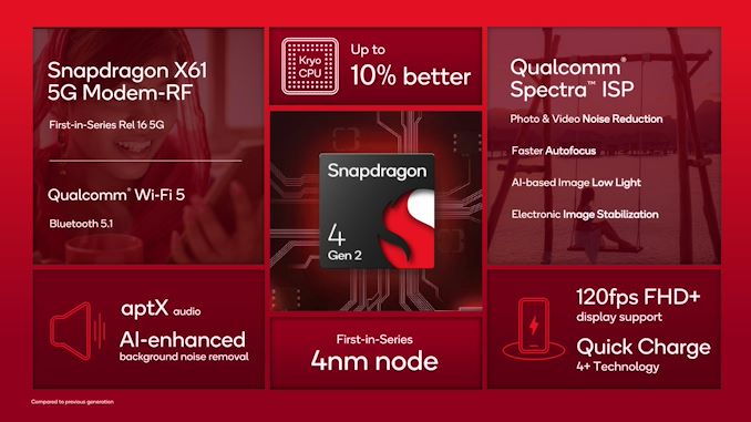
Gallery: Snapdragon 4 Gen 2 Press Deck


More...
-
06-27-23, 09:28 AM #11779
Anandtech: OneOdio OpenRock Pro and Shokz OpenRun Open Ear Headsets Capsule Review
Bone conduction headsets have slowly gained traction in the market over the last decade. Despite technological improvements over multiple generations, the audio quality of in-ear devices that rely on normal air conduction is usually much better. Some vendors have realized the market opportunity in a device that can match desirable qualities from both types of headsets. The last few years have seen the appearance of open-ear air conduction / directional audio headsets that retain the situational awareness advantage (no ear occlusion) while also delivering better audio quality compared to bone conduction devices. One of the recent entrants to this segment is OneOdio's OpenRock Pro. Read on to find out how it stacks up against the AfterShokz Aeropex (now Shokz OpenRun) that relies on bone conduction.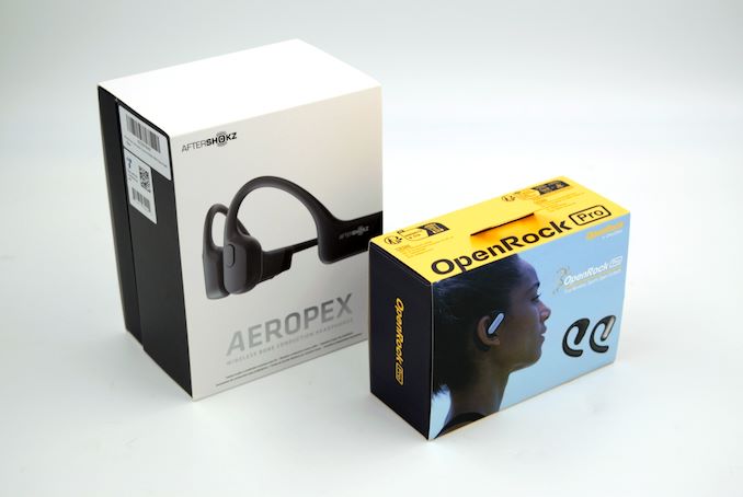
More...
-
06-27-23, 09:28 AM #11780
Anandtech: Seagate Announces FireCuda 540 PCIe Gen5 SSD
Flash-based computer storage has been improving in speed and capacity at breakneck pace over the last decade. M.2 NVMe SSDs have almost completely replaced SATA drives for primary storage capabilities in new systems. While small form-factor machines are continuing to rely on PCIe Gen3 SSDs for an optimal balance of performance and thermal solution sizing, Gen4 SSDs - particularly of the DRAM-less variety - are slowly starting to break into that segment. However, the gaming segment in the consumer market has fueled the need for speed and created a demand for PCIe Gen5 SSDs.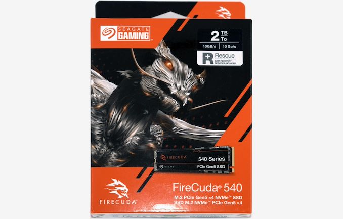
Phison's E26 controller has been ruling the roost in this area, with almost all currently available Gen5 SSDs being based on it. Today, Seagate is announcing the availability of the FireCuda 540 PCIe Gen5 M.2 2280 NVMe SSD. With its PCIe 5.0 x4 interface, there is a marked increase in sequential access speeds over the previous flagship (FireCuda 530). The addition of optimizations for DirectStorage in the firmware makes it an ideal candidate for gaming enthusiasts.
The drives in Seagate's FireCuda SSD series have typically been based on Phison controllers using custom firmware (with the company's preferred term being 'Seagate-validated'), and the FireCuda 540 is no different. It is based on Phison's PS5026-E26 using the latest 3D TLC NAND (Micron's B58R 232L).
Micron's B58R 232L 3D TLC NAND can operate at up to 2400 MT/s, and these transfer rates have been used by some Gen5 SSD vendors to obtain bragging rights for the highest sequential access bandwidth numbers (in the range of 12 - 14 GBps). It appears highly likely that Seagate has decided to operate them at lower speeds and limit the overall maximum sequential rates to around 10 GBps. This should help in both the thermals and power consumption aspects.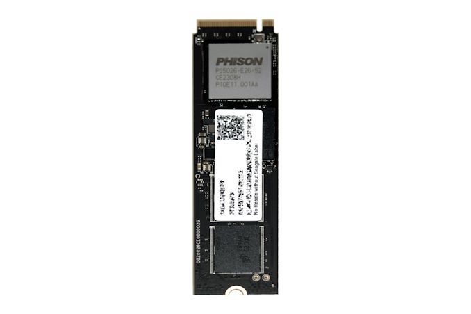
FireCuda 540 : Phison E26 Gen5 Controller + Micron B58R 3D TLC NAND
Unlike other flagship M.2 PCIe 5.0 x4 NVMe SSDs, the FireCuda 540 does not come with a heatsink option. Rather, the company makes it a point to mention that an external cooling solution is necessary for optimal performance. With motherboard vendors offering their own SSD cooling solutions compatible with their board layout, and third-party SSD cooling solutions also in the market, this is probably a good move to keep pricing low.
Seagate is opting to release only 1 TB and 2 TB versions of the FireCuda 540 for now.
Other than DirectStorage optimizations, another key update seems to be the availability of hardware-based TCG Opal Encryption (that was noticeably absent in the FireCuda 530 at launch). The DRAM and flash industry is in one of the troughs of their usual pricing cycles - so this is good news for end consumers (not so much for the flash vendors). At around $150 / TB for the 2TB model, there is nothing to complain about - but do note that this doesn't include a cooling solution (which is mandatory if one is investing in a Gen5 SSD).Seagate FireCuda 540 SSD Specifications Capacity 1 TB 2 TB Controller Phison PS5026-E26 (PCIe 5.0 x4) NAND Flash 232L 3D TLC NAND (Micron B58R) Form-Factor, Interface Single-Sided M.2-2280, PCIe 5.0 x4, NVMe 2.0 Double-Sided M.2-2280, PCIe 5.0 x4, NVMe 2.0 Sequential Read 9500 MB/s 10000 MB/s Sequential Write 8500 MB/s 10000 MB/s Random Read IOPS 1.30 M 1.49 M Random Write IOPS 1.50 M Pseudo-SLC Caching Supported TCG Opal Encryption Yes Power (Active / Standby) 10 W / 144 mW 11 W / 144 mW Warranty 5 years (with 3 year DRS) Write Endurance 1000 TB
0.55 DWPD2000 TB
0.55 DWPDMSRP (non-heatsink) $180 (18¢/GB) $300 (15¢/GB)
More...


 Quote
QuoteThread Information
Users Browsing this Thread
There are currently 23 users browsing this thread. (0 members and 23 guests)


Bookmarks