

Results 11,801 to 11,810 of 12089
Thread: Anandtech News
-
07-17-23, 07:43 PM #11801
Anandtech: Lenovo Develops Mini-ITX Form-Factor GeForce RTX 4060
One of design perks of NVIDIA's GeForce RTX 4060 is its relatively low power consumption, which has allowed graphics cards makers to produce compact add-in-boards without the massive heatsink and VRM setups required by higher-end cards. At 115 Watts, the power consumption of the card is low enough that it makes even Mini-ITX-sized cards practical, which is great news for the SFF PC community. And to that end, we've seen a few manufacturers introduce Mini-ITX GeForce RTX 4060 designs, with Lenovo now joining them as the latest member of the club with their own Mini-ITX 4060 card.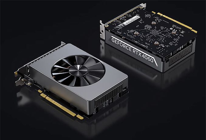
Specifications-wise, Lenovo's Mini-ITX GeForce RTX 4060 is exactly what you'd expect: it a stock-configuration RTX 4060 that carries NVIDIA's AD107 graphics processor with 3072 CUDA cores that is mated to 8 GB of GDDR6 memory using a 128-but interface. Lenovo does not disclose display outputs configuration (though expect both DisplayPort and HDMI to be present), though we see an eight-pin auxiliary PCIe power connector on the back of the board.
Meanwhile, the video card is equipped with a dual-slot, single-fan cooling system, which is typical for cards in this segment. The small heatsink and single fan is a big part in what's enabled Lenovo to build such a small card, ensuring it will fit in a Mini-ITX system (at least so long as it can accept dual-slot cards).
Overall, with its size and scale as the world's largest PC maker, we've seen Lenovo designs and manufacture scores of components over the years for their own internal use, with their Mini-ITX video card being the latest example. For the moment, Lenovo's Mini-ITX GeForce RTX 4060 is exclusively used for the company's IdeaCentre GeekPro 2023 system that is sold on JD.com. The PC is powered by Intel's Core i5-13400F and is outfitted with 16GB of RAM along with a 1TB SSD.
And while Lenovo is only using the card internally for now, there's also a chance the card could eventually make it to retail as a grey market product. The large scale of the company that makes internal component production viable also means that Lenovo parts sometimes end up on etailer shelves, especially if the company has excess stock to move.
More...
-
07-18-23, 12:08 PM #11802
Anandtech: ASRock Industrial NUC BOX-1360P/D5 Review: Raptor Lake-P on the Leading Ed
ASRock Industrial has been a key player in the ultra-compact form-factor PC space over the last few years. They have managed to release 4"x4" systems based on the latest AMD and Intel platforms well ahead of other vendors. The company's NUC BOX-1300 series was launched along with Intel's introduction of Raptor Lake-P in January 2023. The NUCS BOX-1360P/D4 was made available in early February with minimal improvements over the NUC BOX-1200 series. The company reserved the key Raptor Lake-P updates - DDR5 support, and USB 3.2 Gen 2x2 on the Type-C ports for the D5 series. Read on for a detailed investigation into the performance profile and feature set of the NUC BOX-1360P/D5.
More...
-
07-18-23, 12:08 PM #11803
Anandtech: Samsung Foundry's 3nm and 4nm Yields Are Improving - Report
Currently, only two foundries offer their customers 3 nm and 4 nm-class process technologies: TSMC and Samsung Foundry. But business media sometimes blames Samsung Foundry for mediocre yields on leading-edge nodes, which cannot be verified. But a recent report issued by an investment banking firm claims that yields of Samsung's 3 nm and 4 nm-class nodes are on quite decent levels. But there is a catch.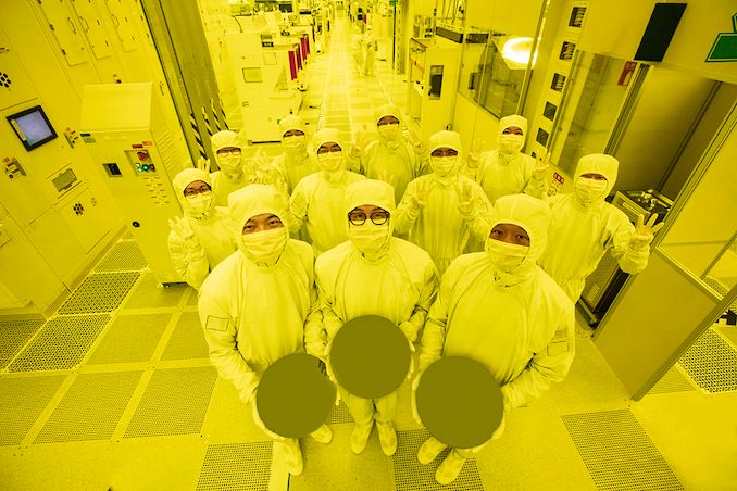
Samsung Foundry's 4 nm-class process technology yield is now higher than 75%. In contrast, yields of chips on SF3E (3nm-class, gate-all-around early) now exceeds 60%, according to estimates in a report from Hi Investment & Securities, a member of DGB Financial Group, reports Kmib.co.kr. The same report claims that TSMC's yields at its N4 node approach 80%, but again, this is an estimate by a researcher.
In general, information about yields at foundries cannot be verified since contract makers of chips never talk about yields publicly since they depend on several things, such as die size, performance targets, and design peculiarities. They sometimes disclose defect density publicly compared to previous nodes, but this is hardly the case for Samsung Foundry's SF4E, SF4, SF4P, and SF3E.
Officially, Samsung Foundry only says that its SF3E process technology is in high-volume production with stable yields (possibly to address a media report from late last year which said that SF's yields on SF3E were unstable), and the development of refined SF3 is ongoing.
"We are mass producing the 1st gen 3nm process with stable yields, and, based on this experience, we are developing the 2nd gen process to secure even greater mass production capabilities," a statement by Samsung reads.
Meanwhile, TechInsights found one of the first chips made on Samsung's SF3E process. This is the Whatsminer M56S++ which is apparently a cryptocurrency mining chip from MicroBT, a Chinese developer. Mining chips are tiny simplistic devices with loads of regular structures and few SRAM bit cells. Such chips are easy to make and serve perfectly as pipe cleaners for the latest process technologies, so it is not surprising that Samsung Foundry is making them rather than large ASICs on its SF3E. Meanwhile, yields of small chips are, by definition, higher than yields of large ASICs made on the same node. Therefore, if yields of the Whatsminer M56S++ are at 75% or higher, it does not mean that a large smartphone or PC SoC yields will be at the same level with the same defect density.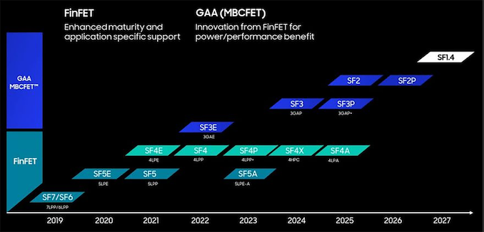
There is an indirect confirmation that yields of Samsung's 5 nm and 7 nm-class fabrication processes are improving. The utilization rate of Samsung Foundry's for 5 nm-capable lines increased to 80%, and the combined utilization rate of 5nm and 7 nm-capable fabs climbed to 90% recently, up from 60% in 2022, according to a DigiTimes story that cites ET News. Again, the information comes from an unofficial source.
Typically, fabless chip designers are not inclined to use nodes with high defect densities, so if the utilization rate of 5 nm-class (Samsung's SF4 derived from SF5) gets higher, this may indicate that they are now more intensively used by Samsung's customers. Alternatively, this may be a sign that Samsung Foundry has customers desperate enough to increase production despite low yields due to high demand. Yet, given the current market conditions, this may not be the case.
Sources: Kmib.co.kr, DigiTimes, TechInsights
Gallery: Samsung Foundry's 3nm, 4nm Yields Are Improving Rapidly Report

More...
-
07-18-23, 10:39 PM #11804
Anandtech: Samsung Completes Initial GDDR7 Development: First Parts to Reach Up to 32
Samsung has announced this evening that they have completed development on their first generation of GDDR7 memory. The next iteration of the high bandwidth memory technology, which has been under industry-wide development, is expected to hit the market in 2024, with Samsung in prime position to be one of the first memory vendors out of the gate. With their first generation of GDDR7 parts slated to hit up to 32Gbps/pin of bandwidth – 33% more than their best GDDR6 parts today – the company is looking to deliver a sizable increase in GDDR memory bandwidth on the back of the technology’s adoption of PAM-3 signaling.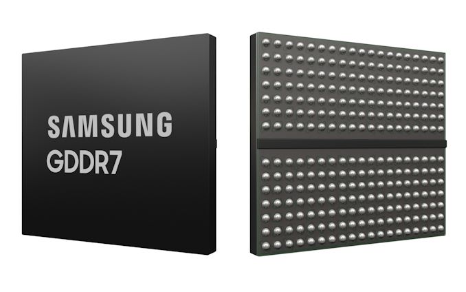
Samsung’s announcement comes as we’ve been seeing an increase in disclosures and announcements around the next iteration of the widely-used memory technology. While a finished specification for the memory has yet to be released by JEDEC, Samsung rival Micron has previously announced that it plans to introduce its own GDDR7 memory in 2024 – a similar timeline as to Samsung’s current schedule. Meanwhile, EDA tool firm Cadence disclosed a significant amount of technical details earlier this year as part of announcing their GDDR7 verification tools, revealing that the memory would use PAM-3 signaling and reach data rates of up to 36Gbps/pin.
With today’s announcement, Samsung has become the first of the major memory manufacturers to publicly announce that they’ve completed development of their first generation of GDDR7. And while the company tends to make these sorts of memory announcements relatively early in the bring-up process – well before memory is ready for commercial mass product – it’s none the less an important milestone in the development of GDDR7, as it means that memory and device manufacturers can begin validation work against functional hardware. As for Samsung itself, the announcement gives the Korean conglomerate a very visible opportunity to reinforce their claim of leadership within the GDDR memory industry.
Besides offering an update on the development process for GDDR7, Samsung’s announcement also provides some high-level technical details about the company’s first generation of GDDR7 – though “high-level” is the operative word as this is not by any means a technical deep dive.
According to Samsung’s announcement, they’re expecting to reach data rates as high as 32Gbps/pin. That’s 33% higher than the 24Gbps data rate the company’s top GDDR6 products can hit today. Samsung and Cadence have both previously disclosed that they expect GDDR7 memory to eventually hit 36Gbps/pin, though as with the development of GDDR6 – a full 50% faster than GDDR6 – this is likely going to take multiple generations of products.GPU Memory Math GDDR7 GDDR6X GDDR6 B/W Per Pin 32 Gbps (Projected) 24 Gbps (Shipping) 24 Gbps (Sampling) Chip Density 2 GB (16 Gb) 2 GB (16 Gb) 2 GB (16 Gb) Total B/W (256-bit bus) 1024 GB/sec 768 GB/ssec 768 GB/ssec DRAM Voltage ? 1.35 V 1.35 V Data Rate QDR QDR QDR Signaling PAM-3 PAM-4 NRZ (Binary) Packaging 266 FBGA 180 FBGA 180 FBGA
Interestingly, this is starting much closer to projected limits of GDDR7 than we’ve seen in past generations of the memory technology. Whereas GDDR6 launched at 14Gbps and eventually scaled up to 24Gbps, Samsung wants to start at 32Gbps. At the same time, however, GDDR7 is going to be a smaller generational leap than we saw for GDDR6 or GDDR5; rather than doubling the signaling bandwidth of the memory technology over its predecessor, GDDR7 is only a 50% increase, owing to the switch from NRZ (2 state) signaling to PAM-3 (3 state) signaling.
It’s also worth noting that, at present, the fastest GDDR6 memory we see used video cards is only running at 20Gbps.Samsung’s own 24Gbps GDDR6, though announced just over a year ago, is still only “sampling” at this time. So the multitude of other GDDR6-using products notwithstanding, the effective jump in bandwidth for video cards in 2024/2025 could be more significant, depending on just what speed grades are available at the time.
As for capacity, Samsung’s first GDDR7 chips are 16Gb, matching the existing density of today’s top GDDR6(X) chips. So memory capacities on final products will not be significantly different from today’s products, assuming identical memory bus widths. DRAM density growth as a whole has been slowing over the years due to scaling issues, and GDDR7 will not be immune to that.
Samsung is also claiming that their GDDR7 technology offers a “20%-improvement in power efficiency versus existing 24Gbps GDDR6 DRAM,” though this is a broad claim where the devil is in the details. As power efficiency for DRAM is normally measured on a per-bit basis (picojoules-per-bit/pJpb), then our interpretation is that this is the figure Samsung is referencing in that claim. But whether that measurement is being made at 24Gbps (iso-bandwidth) or 32Gbps remains unclear.
Either way, the good news is that Samsung’s GDDR7 is slated to deliver a tangible increase in energy efficiency. But at only a 20% improvement in energy efficiency for a memory technology that is delivering up to 33% more bandwidth, this means that the absolute power consumption of the memory is going up versus the previous generation. Assuming Samsung’s energy efficiency figures are for GDDR7@32Gbps versus GDDR6@24Gbps, then we’d be looking at around a 7% increase in total energy consumption. Otherwise, if it’s at iso-bandwidth, then the increase in power consumption at full bandwidth could be much higher, depending on just what Samsung’s voltage/frequency curve comes out to.
Broadly speaking, this is the same outcome as we saw with the introduction of GDDR6(X), where despite the energy efficiency gains there, overall power consumption increased from one generation to the next, as energy efficiency gains are not keeping pace with bandwidth demands. Not to say that any of this is unexpected, but it means that good cooling will be even more critical for GDDR7 memory.
But for clients with strict power/cooling needs, Samsung is also announcing that they will be making a low-voltage version of their GDDR7 memory available. The company has not disclosed the nominal voltage of their GDDR7, or of its low-voltage counterpart, but we’d expect to see Samsung using the same chips clocked lower in exchange for a lower operating voltage, similar to low-voltage GDDR6.
Also missing from Samsung’s disclosure is anything on the fab process they’re using to produce the new memory. The company’s most recent GDDR6 uses their D1z process, while a recent DDR5 memory announcement from Samsung has them using their 12nm (D1b?) there. Even if we don’t know the specific node in use, Samsung is almost certainly using a newer node for GDDR7. Which means that at least some of the 20% energy efficiency gains from GDDR7 are going to be a product of the newer node, rather than intrinsic efficiency improvements from GDDR7.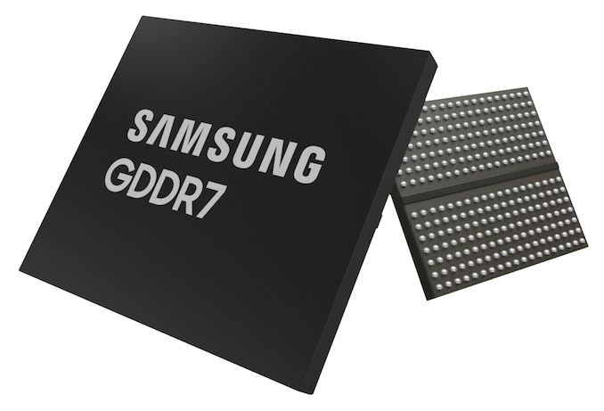
Though Samsung certainly has been working on those, as well. While again quite light in details, the company notes that their GDDR7 memory employs “IC architecture optimization” to keep power and heat generation in check.
Electronics production aside, the final major innovation with Samsung’s GDDR7 will be decidedly physical: epoxy. Clearly mindful of the already high heat loads generated by existing GDDR memory clocked at its highest speeds, Samsung’s press release notes that they’re using a new epoxy molding compound (EMC) for GDDR7, which is designed to better transfer heat. All told, Samsung is claiming a 70% reduction in thermal resistance versus their GDDR6 memory, which should help ensure that a good cooler can still pull enough heat from the memory chips, despite the overall increase in heat generation.
Wrapping things up, now that initial development on their GDDR7 memory has been completed, Samsung is moving on to verification testing with their partners. According to the company, they’ll be working with key customers on verification this year; though at this point, the company isn’t saying when they expect to kick off mass production of the new memory.
Given the timing of Samsung’s announcement (as well as Micron’s), the initial market for GDDR7 seems to be AI and networking accelerators, rather than the video cards that GDDR7 gets its name from. With both AMD and NVIDIA barely a quarter of the way through their current architectural release cycles, neither company is likely be in a position to use GDDR7 in 2024 when it’s ready. Instead, it’s going to be the other users of GDDR memory such as networking products and high-performance accelerators that are likely to be first to use the technology.
Gallery: Samsung GDDR7 Chip Renders


More...
-
07-18-23, 10:39 PM #11805
Anandtech: Logitech Acquires Loupedeck to Enhance Its Software Roadmap
Being a significant maker of peripherals in general and gaming peripherals in particular, Logitech cannot omit the content creators and streamers market, which is now virtually dominated by Corsair's Elgato. On Tuesday, Logitech said that it had acquired Loupedeck, a streaming controller specialist, enabling the company to address streamers with a dedicated product. Furthermore, the company plans to use Loupedeck's expertise beyond its controllers.
Streaming controllers is a dynamically developing and lucrative market. These controllers retail sold for $199 - $499 per unit, and the company also makes Stream Controller for Razer, which it is set to continue building even after it becomes a part of Logitech. Meanwhile, the latter gets a potentially profitable business with many opportunities beyond the gaming market.
Loupedeck's streaming controllers are versatile devices that run proprietary multifaceted software that supports game streaming tools like OBS, Twitch, vMix, and Ecamm Live and applications widely used by content producers. The list includes programs like Adobe Photoshop, Adobe Premiere Pro, Adobe After Effects, Final Cut Pro, and Philips Hue Bridge. They also support tens of profiles to adjust for applications and can be used for content creation flows outside the game streaming world.
The Loupedeck Live S Streaming Console
Loupedeck's integration strengthens Logitech's ability to offer creative tools for a diverse user base, including gamers, live-streamers, YouTubers, and other creative professionals. The two companies share a skillset for creating products integrating hardware and software, though it remains to be seen how Logitech plans to use Loupedeck's expertise. The company says the takeover will enhance its ability to deliver personalized and context-sensitive control experiences across all its devices. This may indicate that Loupedeck's devices will continue to deliver on their promise or may imply that Loupedeck's expertise will be used beyond its controllers.
"This acquisition augments Logitech's product portfolio today and accelerates our software ambitions of enabling keyboards, mice, and more to become smarter and contextually aware, creating a better experience for audiences across Logitech," said Ujesh Desai, general manager of Logitech G, the company's gaming unit.
One crucial detail is that Logitech plans to engage and support Loupedeck's expanding developer community to spur additional innovation from third parties.
"Joining Logitech allows us to elevate what we are doing to the next level and exponentially broaden our audience and our impact to the creative process," said Mikko Kesti, Loupedeck's chief executive officer.
More...
-
07-19-23, 09:34 AM #11806
Anandtech: ASUS Signs Agreement to Continue Development and Support of Intel's NUC Bu
ASUS and Intel late on Tuesday announced that they had agreed to a term sheet involving Intel's NUC business, ensuring the continued support of existing NUC hardware as well as the development of new designs. Under the terms of the deal, ASUS will receive a non-exclusive license to existing Intel's NUC systems designs, the right to develop future designs, and an obligation to support existing NUCs. The world's largest motherboard supplier and one of the top 10 PC makers will thus take over a significant portion of the NUC program.
"As we pivot our strategy to enable ecosystem partners to continue NUC systems product innovation and growth, our priority is to ensure a smooth transition for our customers and partners," said Sam Gao, Intel vice president and general manager of Intel Client Platform Solutions. "I am looking forward to ASUS continuing to deliver exceptional products and supporting our NUC systems customers."
"Thank you, Intel, for your confidence in us to take the NUC systems product line forward," said Joe Hsieh, ASUS chief operating officer. "I am confident that this collaboration will enhance and accelerate our vision for the mini PC – greatly expanding our footprint in areas such as AI and AioT. We are committed to ensuring the excellent support and service that NUC systems customers expect."
The move comes as Intel last week announced that the company will be exiting the NUC business – one of several strategic shuffles made by Intel in the past couple of years that has seen the company exit many of its non-core businesses. With Intel doubling down on chip design and fabrication, these business units have frequently been sold to other parties, such as Intel's SSD/NAND business (now Solidigm/SK hynix) and Intel's pre-built server business (now MiTAC).
Under the terms of the proposed deal, ASUS will form a new business unit called ASUS NUC, which will be able to produce and sell Intel's 10th through 13th generation NUC PCs, as well as rights to develop future NUC designs. The deal also obligates ASUS to provide support for the platform, with Intel and ASUS both reiterating the importance of continued support (and business continuity) of the platform.
Curiously, the deal is explicitly nonexclusive; so despite ASUS being set up to be Intel's successor in the NUC space, ASUS isn't necessarily getting the NUC market to itself – though Intel isn't announcing any other licensees at this time, either. The limited details on the deal also do not mention ASUS taking on any employees from Intel's existing NUC group, so it seems this will not be a wholesale business unit transfer like other units such as SSDs have been.
In any case, licensing Intel's NUC business should greatly strengthen ASUS's position within the compact PC market. Even with their vast engineering resources and a broad lineup of products, ASUS has only offered a limited range of NUC-sized PC products. The company currently offers its PN and PB series of mini-PCs, along with some ExpertCenter desktop models that fit in the SFF category. The PN series could be termed as clones of the mainstream NUCs, and ASUS has a wide variety of notebooks that probably render the NUC Laptop Kits irrelevant. However, ASUS currently doesn't have equivalents of the NUC Enthusiast and NUC Extreme models or the NUC Compute Elements.
Ultimately, those NUC products will be complementary to ASUS's current lineup of mini-PCs and SFF systems, allowing ASUS to grow its overall footprint in the compact PC space. The deal is also a win for the existing NUC ecosystem, as current users are assured of support and warranties will continue to get honored.
Looking forward, there is plenty of scope for continued innovation in the NUC space under ASUS. For example, allowing USB-C PD to power the NUCs, or even PoE support for the NUCs targeting industrial applications, are low-hanging fruits. ASUS is probably among the few companies in the world that can afford to continue to innovate while running the current program at scale.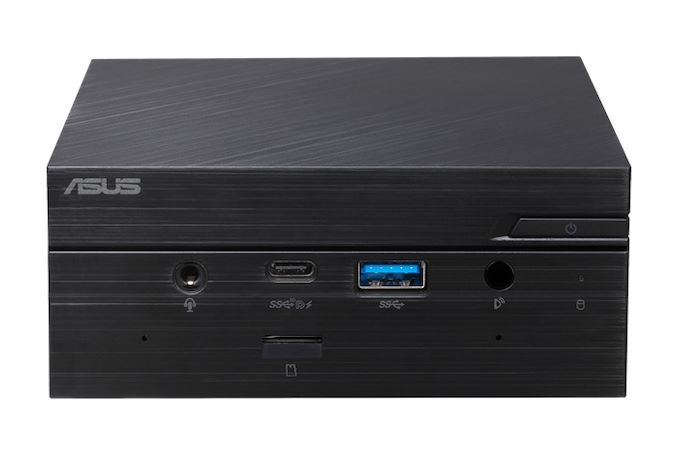
The PN Mini-PC Series - NUC Mainstream's ASUS Avatar
One big question is who will be producing existing and future NUCs. Intel outsourced at least some of its NUCs to third parties like ECS and Pegatron under OEM deals, which is a normal practice. By contrast, ASUS outsources a significant portion of its production to Pegatron, its daughter company. We do not know who exactly produces the 10th - 13th Gen. NUCs for Intel at the moment, but if it is not Pegatron, it remains to be seen whether ASUS will continue to order systems from the current supplier, or will try to transfer production to its usual manufacturing partner.
More...
-
07-20-23, 11:04 AM #11807
Anandtech: Solidigm Announces D5-P5336: 64 TB-Class Data Center SSD Sets NVMe Capacit
Advancements in flash technology have come as a boon to data centers. Increasing layer counts coupled with better vendor confidence in triple-level (TLC) and quad-level cells (QLC) have contributed to top-line SSD capacities essentially doubling every few years. Data centers looking to optimize storage capacity on a per-rack basis are finding these top-tier SSDs to be an economically prudent investment from a TCO perspective.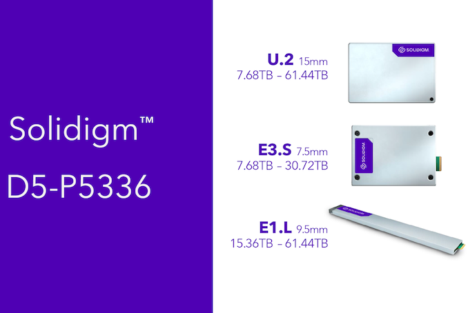
Solidigm was one of the first vendors to introduce a 32 TB-class enterprise SSD a few years back. The D5-P5316 utilized Solidigm's 144L 3D QLC NAND. The company has been extremely bullish on QLC SSDs in the data center. Compared to other flash vendors, the company has continued to use a floating gate cell architecture while others moved on to charge trap configurations. Floating gates retain programmed voltage levels for a longer duration compared to charge trap (ensuring that the read window is much longer without having to 'refresh' the cell). The tighter voltage level retaining capability of the NAND architecture has served Solidigm well in bringing QLC SSDs to the enterprise market.
Solidigm is claiming that their 192L 3D QLC is extremely competitive against TLC NAND from its competitors that are currently in the market (read, Samsung's 136L 6th Gen. V-NAND and Micron's 176L 3D TLC).
Solidigm segments their QLC data center SSDs into the 'Essential Endurance' and 'Value Endurance' lines. Back in May, the company introduced the D5-P5430 as a drop-in replacement for TLC workloads. At that time, the company had hinted at a new 'Value Endurance' SSD based on their fourth generation QLC flash in the second half of the year. The D5-P5336 announced recently is the company's latest and greatest in the 'Value Endurance' line.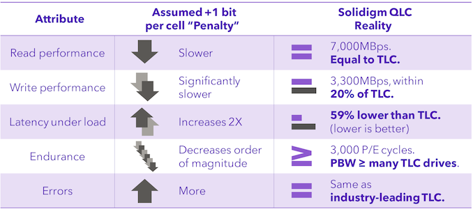
The D5-P5316 used a 64KB indirection unit (IU) (compared to the 4KB used in normal TLC data center SSDs). While endurance and speeds were acceptable for specific types of workloads that could avoid sub-64KB writes, Solidigm has decided to improve matters by opting for a 16KB IU in the D5-P5336.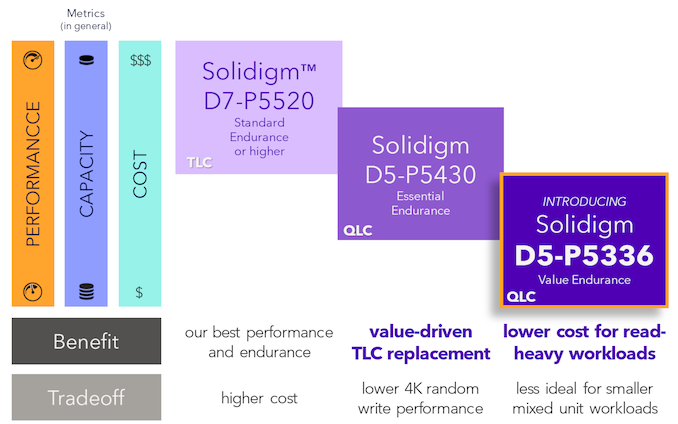
Solidigm's 2023 Data Center SSD Flagships by Market Segment
Thanks to the increased layer count, Solidigm is able to offer the D5-P5336 in capacities up to 61.44 TB. This takes the crown for the highest capacity in a single NVMe drive, allowing a single 1U server with 32 E1.L versions to hit 2 PB. For a 100 PB solution, Solidigm claims up to 17% lower TCO against the best capacity play from its competition (after considering drive and server count as well as total power consumption).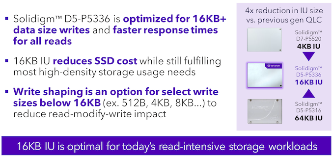
Note that Solidigm is stressing endurance and performance numbers for IU-aligned workloads. Many of the interesting aspects are not yet known as the product brief is still in progress.Solidigm D5-P5336 NVMe SSD Specifications Aspect Solidigm D5-P5336 Form Factor 2.5" 15mm U.2 / 7.5mm E3.S / 9.5mm E1.L Interface, Protocol PCIe 4.0 x4 NVMe 1.4c Capacities U.2
7.68 TB, 15.36 TB, 30.72 TB, 61.44 TBE3.S
7.68 TB, 15.36 TB, 30.72 TBE1.L
15.36 TB, 30.72 TB, 61.44 TB3D NAND Flash Solidigm 192L 3D QLC Sequential Performance (GB/s) 128KB Reads @ QD 128 7.0 128KB Writes @ QD 128 3.3 Random Access (IOPS) 4KB Reads @ QD 256 1005K 16KB Writes @ QD 256 43K Latency (Typical) (us) 4KB Reads @ QD 1 ?? 4KB Writes @ QD 1 ?? Power Draw (Watts) 128KB Sequential Read ?? 128KB Sequential Write 25.0 4KB Random Read ?? 4KB Random Write ?? Idle 5.0 Endurance (DWPD) 100% 128KB Sequential Writes ?? 100% 16KB Random Write 0.42 (7.68 TB) to 0.58 (61.44 TB) Warranty 5 years
Ultimately, the race for the capacity crown comes with tradeoffs. Similar to hard drives adopting shingled-magnetic recording (SMR) to eke out extra capacity at the cost of performance for many different workload types, Solidigm is adopting a 16KB IU with QLC NAND optimized for read-intensive applications. Given the massive capacity per SSD, we suspect many data centers may find it perfectly acceptable (at least, endurance-wise) to use it in other workloads where storage density requirements matter more than write performance.
Gallery: Solidigm Announces D5-P5336: 64 TB-Class Data Center SSD Sets NVMe Capacity Records


More...
-
07-20-23, 11:04 AM #11808
Anandtech: TSMC Delays Arizona Fab Deployment to 2025, Citing Shortage of Skilled Wor
TSMC on Thursday disclosed that it will have to delay mass production at its Fab 21 in Arizona to 2025, as a lack of suitably skilled workers is slowing down the installation of cleanroom tools. The company also confirmed that it is sending in hundreds of people familiar with its fabs from Taiwan to Arizona to assist the installation.
"We are encountering certain challenges, as there is an insufficient amount of skilled workers with the specialized expertise required for equipment installation in a semiconductor-grade facility," said Mark Liu, chairman of TSMC, during the company's earnings call with financial analysts and investors. "While we are working on to improve the situation, including sending experienced technicians from Taiwan to train local skill workers for a short period of time, we expect the production schedule of N4 process technology to be pushed out to 2025."
Construction of TSMC's Fab 21 phase 1 kicked off in April 2021, and reached completion a little behind schedule by the middle of 2022. In December of 2022, TSMC started moving equipment in. Normally, equipping a fab's cleanroom requires around a year, which is why TSMC anticipated that the chip manufacturing plant would be operational by early 2024. Apparently, installation of production tools into Fab 21 encountered several setbacks as local workers were unfamiliar with TSMC's requirements.
As it turns out, these setbacks were so severe that TSMC now expects to need an extra year to start mass production at the fab, moving the start date from early 2024 to 2025. Which, at what's now 18+ months out, TSMC isn't even bothering to provide guidance about when in 2025 it expects its Fab 21 phase 1 to start mass production – only that it will happen at some point in the year.
The impact of TSMC's Fab 21 launch delay on its U.S. customers is yet to be determined. The megafab-class facility is not nearly as large as TSMC's flagship gigafabs in Taiwan, so the impact in terms of wafer starts is not as significant as if one of the larger fabs was delayed. The most recent estimate for Fab 21 was that it would hit 20K wafer starts per month, around one-fifth the capacity of a gigafab. So the capacity loss, while important, is not critical to TSMC's overall production quotas. Though with TSMC expecting to be at full capacity in 2024, there may not be much capacity left to pick up the slack.
Likely to be the bigger concern is that Fab 21 was being built (and subsidized) in large part to allow TSMC to produce sensitive, US-based chip designs within the US. While non-sensitive chips can be allocated to other fabs in Taiwan (capacity permitting), that's not going to be a suitable alternative for chips that need to be built within the US. A one-year delay on Fab 21 is likely to throw a wrench into those plans, but it will be up to TSMC's buyers (and their government clients) on whether to accept the delay or look at alternatives.
Finally, getting back to the subject of skilled workers, late last month TSMC confirmed to Nikkei that it was in talks with the U.S. government to provide non-immigrant visas to its Taiwanese specialists to the U.S., to help at "a critical phase, handling all of the most advanced and dedicated equipment in a sophisticated facility." According to the Nikkei report, a 500-man team of technicians was dispatched from Taiwan, arriving with hands-on expertise in a diverse range of fields. This expertise includes the installation of wafer fab tools and their synchronized operation, and, among other things, construction of fab mechanical and electrical systems.
Sources: TSMC, Nikkei
More...
-
07-21-23, 11:09 AM #11809
Anandtech: Ultra Ethernet Consortium Formed, Plans to Adapt Ethernet for AI and HPC N
This week the Linux Foundation has announced that the group will be overseeing the formation of a new Ethernet consortium, with a focus on adapting and refining the technology for high performance computing workloads. Backed by founding members AMD, Arista, Broadcom, Cisco, Eviden, HPE, Intel, Meta and Microsoft, the new Ultra Ethernet Consortium will be working to improve Ethernet to meet the low latency and scalability requirements that HPC and AI systems need – and which the group says current Ethernet technology isn't quite up to the task for.
The top priority of the new group will be to define and develop what they are calling the Ultra Ethernet Transport (UET) protocol, a new transport-layer protocol for Ethernet that will better address needs of AI and then HPC workloads.
Ethernet is certainly one of the most ubiquitous technologies around, but demands of AI and HPC clusters are growing so fast that the technology will run out of steam in the future. The size of large AI models is increasing rapidly. GPT-3 was trained with 175 billion of parameters back in 2020. Today GPT-4 is said to be accommodating already a trillion of parameters. Models with the larger number of parameters require larger clusters and then these clusters send larger messages over the network. As a result, the higher bandwidth and the shorter latency these network feature, the more efficient the cluster can operate.
"Many HPC and AI users are finding it difficult to obtain the full performance from their systems due to weaknesses in the system interconnect capabilities," said Dr. Earl Joseph, CEO of Hyperion Research.
At a high level, the new Ultra Ethernet Consortium is looking to refine Ethernet in a surgical manner, improving and altering only those bits and pieces necessary to achieve their goals. At its onset, the consortium is looking at improving both the software and physical layers of Ethernet technology — but without altering its basic structure to ensure cost efficiency and interoperability.
Technical goals of the consortium include developing specifications, APIs, and source code to define protocols, interfaces, and data structures for Ultra Ethernet communications. In addition, the consortium aims to update existing link and transport protocols and create new telemetry, signaling, security, and congestion mechanisms to better address needs of large AI and HPC clusters. Meanwhile, since AI and HPC workloads have a number of differences, UET will have separate profiles for appropriate deployments.
"Generative AI workloads will require us to architect our networks for supercomputing scale and performance," said Justin Hotard, executive vice president and general manager, HPC & AI, at Hewlett Packard Enterprise. "The importance of the Ultra Ethernet Consortium is to develop an open, scalable, and cost-effective ethernet-based communication stack that can support these high-performance workloads to run efficiently. The ubiquity and interoperability of ethernet will provide customers with choice, and the performance to handle a variety of data intensive workloads, including simulations, and the training and tuning of AI models."
The Ultra Ethernet Consortium is hosted by the Linux Foundation, though the real work will be undertaken by its members. Between AMD, Cisco, Intel, and other founders, these companies all either design high-performance CPUs, compute GPUs, and network infrastructure for AI and HPC workloads or build supercomputers or clusters for AI and HPC applications, thus have plenty of experience with appropriate technologies. The work of UEC is set to be conducted by four working groups that will work on Physical Layer, Link Layer, Transport Layer, and Software Layer.
And while the group is not explicitly talking about Ultra Ethernet in relation to any competing technologies, the members of the founding board – or rather, who's not a founding member – is telling. The performance goals and HPC focus of Ultra Ethernet would have it coming into direct competition with InfiniBand, which has for over a decade been the networking technology of choice for low-latency, HPC-style networks. While developed by its own trade association, NVIDIA is said to have an outsized influence on the group vis-a-vie their Mellanox acquisition a few years ago, and they are noticeably the odd man out of the new group. The company makes significant use of both Ethernet and InfiniBand internally, using both for their scalable DGX SuperPod systems.
As for the proposed Ultra Ethernet standards, UEC members are already plotting plans how to integrate the upcoming UET technology into their products.
"We are particularly encouraged by the improved transport layer of UEC and believe our portfolio is primed to take advantage of it," said Mark Papermaster, CTO of AMD in a blog post. "UEC allows for packet-spraying delivery across multiple paths without causing congestion or head-of-line blocking, which will enable our processors to successfully share data across clusters with minimal incast issues or the need for centralized load-balancing. Lastly, UEC accommodates built-in security for AI and HPC workloads that in turn help AMD capitalize on our robust security and encryption capabilities."
Meanwhile, for now UEC does not say when it expects to finalize the UET specification. It's expected that the group will seek certification from the IEEE, who maintains the various Ethernet standards, so there is an additional set of hoops to jump through there.
Finally, the UEC has noted that it is looking for additional members to round out the group, and will begin accepting new member applications from Q4 2023. Along with NVIDIA, there are several other tech giants involved in AI or HPC work that are not part of the group, so that would be their next best chance to join the consortium.
Source: The Linux Foundation, The Register
More...
-
07-21-23, 11:09 AM #11810
Anandtech: Cerebras to Enable 'Condor Galaxy' Network of AI Supercomputers: 36 ExaFLO
Cerebras Systems and G42, a tech holding group, have unveiled their Condor Galaxy project, a network of nine interlinked supercomputers for AI model training with aggregated performance of 36 FP16 ExaFLOPs. The first supercomputer, named Condor Galaxy 1 (CG-1), boasts 4 ExaFLOPs of FP16 performance and 54 million cores. CG-2 and CG-3 will be located in the U.S. and will follow in 2024. The remaining systems will be located across the globe and the total cost of the project will be over $900 million.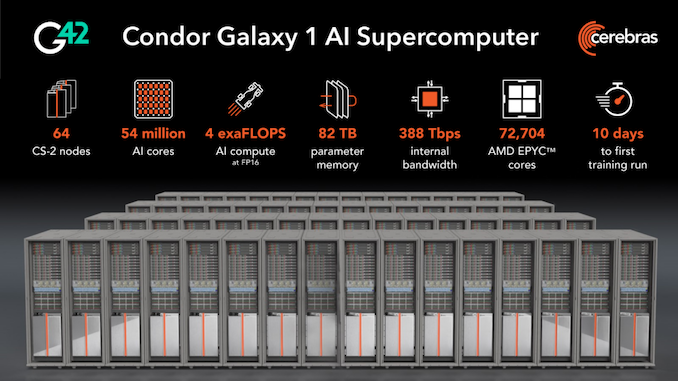
The CG-1 supercomputer, situated in Santa Clara, California, combines 64 Cerebras CS-2 systems into a single user-friendly AI supercomputer, capable of providing 4 ExaFLOPs of dense, systolic FP16 compute for AI training. Based around Cerebras's 2.6 trillion transistor second-generation wafer scale engine processors, the machine is designed specifically for Large Language Models and Generative AI. It supports up to 600 billion parameter models, with configurations that can be expanded to support up to 100 trillion parameter models. Its 54 million AI-optimized compute cores and massivefabric network bandwidth of 388 Tb/s allow for nearly linear performance scaling from 1 to 64 CS-2 systems, according to Cerebras.
The CG-1 supercomputer also offers inherent support for long sequence length training (up to 50,000 tokens) and does not require any complex distributed programming languages, which is common in case of GPU clusters.
“Delivering 4 exaFLOPs of AI compute at FP16, CG-1 dramatically reduces AI training timelines while eliminating the pain of distributed compute,” said Andrew Feldman, CEO of Cerebras Systems. “Many cloud companies have announced massive GPU clusters that cost billions of dollars to build, but that are extremely difficult to use. Distributing a single model over thousands of tiny GPUs takes months of time from dozens of people with rare expertise. CG-1 eliminates this challenge. Setting up a generative AI model takes minutes, not months and can be done by a single person. CG-1 is the first of three 4 ExaFLOP AI supercomputers to be deployed across the U.S. Over the next year, together with G42, we plan to expand this deployment and stand up a staggering 36 exaFLOPs of efficient, purpose-built AI compute.”
This supercomputer is provided as a cloud service by Cerebras and G42 and since it is located in the U.S., Cerebras and G42 assert that it will not be used by hostile states.
CG-1 is the first of three 4 FP16 ExaFLOP AI supercomputers (CG-1, CG-2, and CG-3) created by Cerebras and G42 in collaboration and located in the U.S. Once connected, these three AI supercomputers will form a 12 FP16 ExaFLOP, 162 million core distributed AI supercomputer, though it remains to be seen how efficient this network will be.
In 2024, G42 and Cerebras plan to launch six additional Condor Galaxy supercomputers across the world, which will increase the total compute power to 36 FP16 ExaFLOPs delivered by 576 CS-2 systems.
The Condor Galaxy project aims to democratize AI by offering sophisticated AI compute technology in the cloud.
Sources: Cerebras, EE Times.
More...


 Quote
Quote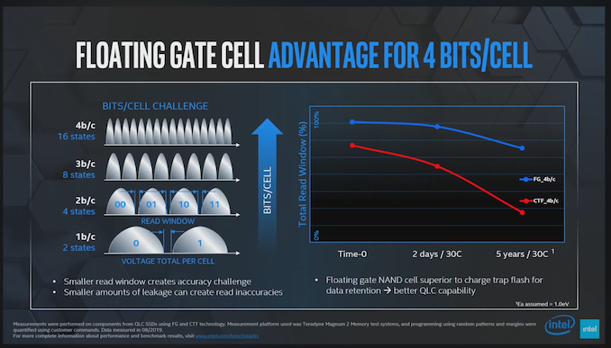
Thread Information
Users Browsing this Thread
There are currently 17 users browsing this thread. (0 members and 17 guests)


Bookmarks