

Results 11,821 to 11,830 of 12089
Thread: Anandtech News
-
07-28-23, 04:53 PM #11821
Anandtech: Dozens of Companies Adopt TSMC's 3nm Process Technology
Designing chips for modern, leading-edge manufacturing technologies is an expensive endeavor. Still, dozens of companies have already adopted TSMCs N3 and N3E (3 nm-class) fabrication processes, according to disclosures made by TSMC and Synopsys.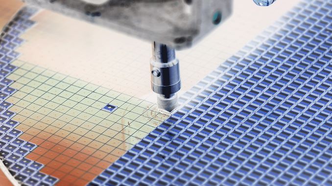
"Synopsys IP for TSMC's 3nm process has been adopted by dozens of leading companies to accelerate their development time, quickly achieve silicon success and speed their time to market," said John Koeter, senior vice president of marketing and strategy for IP at Synopsys.
TSMC has been producing chips using its latest N3 (aka N3B) fabrication technology (with up to 25 EUV layers and support for EUV double patterning) since late 2022 and intends to start making products on its simplified N3E manufacturing process (with up to 19 EUV layers and without EUV double patterning) in Q4 2023.
Previously, TSMC disclosed that its N3 nodes had been adopted by designers of high-performance computing (HPC) and smartphone SoCs and that the number of adopters was higher compared to N5 early in its lifecycle. Meanwhile, TSMC never mentioned the number of companies that had decided to use its 3 nm-class fabrication processes.
Synopsys is a major IP developer and electronic design automation tools provider, so it means a lot when it says that dozens of companies have licensed its IP for TSMC's N3 fabrication technologies. But Synopsys is not the only IP designer out there, and companies like Cadence also supplied their N3-compatible IP to other fabless chip developers. It is safe to say that the number of their clients is also significant.
TSMC's N3 family of process technologies includes baseline N3 (N3B), relaxed N3E with a bit reduced transistor density but widened process window for better yields, performance-enhanced N3P that is IP compatible with N3E will be production ready in the second half of 2024, and N3X for extremely high-performance applications that are due in 2025.
The IP licensed by Synopsys right now can be used for N3, N3E, and N3P production nodes.
Sources: Synopsys
More...
-
07-28-23, 04:53 PM #11822
Anandtech: Samsung Begins to Produce Third 3nm Chip Amid Massive Losses On DRAM & NAN
Samsung this week reported their financial results for the second quarter of 2023, closing the book on an especially bleak quarter of the year with a massive $3.4 billion operating loss. The losses, stemming from its semiconductor business, come amid a continued slump in 3D NAND and DRAM sales volumes and prices. Though buried deep in Samsung's earnings report was a speck of good news, as well: the company has started to produce its third 3nm chip design with stable yield.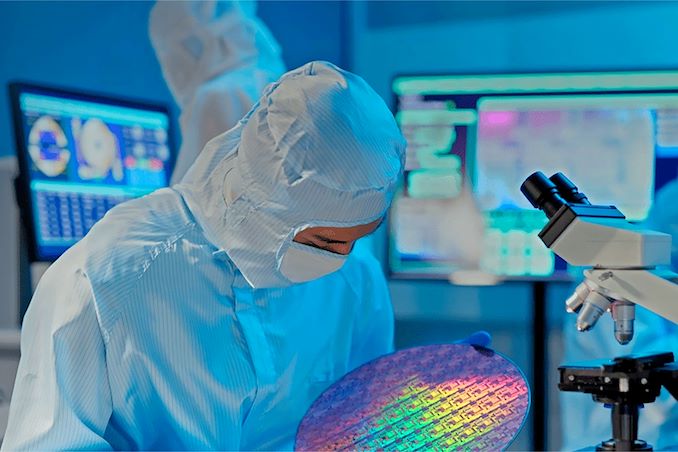
Discussing Samsung Foundry's earnings, the company remains uncertain about demand recovery in the second half. "Demand to recover gradually under considerable uncertainty over the intensity of a market recovery in 2H, with consumer sentiment to rebound amid easing inflation and as customers wind down inventory adjustments," a statement by Samsung reads.
More broadly, Samsung revenue dropped sharply, with the company recording a 22% year-over-year decline to $46.915 billion. Earnings of Samsung's semiconductor divisions — including memory, SoCs, and foundry operations — declined to $29.86 billion, 48% YoY drop. Sales of memory hit $7 billion, a 57% year-over-year decline, though eking out a 1% quarter-over-quarter increase. Overall, Samsung recorded a $3.4 billion loss from its semiconductor operations due to low demand for commodity memory and declining commodity 3D NAND and DRAM prices.
But there were some bright spots in Samsung's DRAM business, as well. Demand for high-performance high-density premium products like DDR5 modules and HBM memory increased, which helped to partly offset slow sales of commodity memory.
"Bit growth exceeded guidance as we expanded sales of server products while actively responding to rising demand for DDR5 and AI-use HBM," Samsung said. "Demand for high-density/high-performance products stayed strong, driven by increased investments focusing on AI by major hyperscalers."
While Samsung expects demand for memory to recover in the second half, the company is expecting to enact additional production cuts to further support memory prices.
"We expect to see a gradual recovery of the memory market in the second half of the year, but the pace of the market rebound is likely to depend on our macro variables," said Jaejune Kim, executive vice president of memory division. "
Kim said that Samsung would be making further alterations to the output of some products, including 3D NAND.
"Production cuts across the industry are likely to continue in the second half, and demand is expected to gradually recover as clients continue to destock their (chip) inventory," a statement by Samsung reads.
Finally, as noted earlier, as part of Samsung's earnings report the company also revealed that it's started production on its third 3nm (GAAFET) chip.
"Mass production of our third GAA product is going smoothly thanks to the stabilization of the 3nm process, and we are developing an improved process for 3nm as planned based on mass production experience with GAA," a statement by Samsung reads.
It recently transpired that Samsung Foundry has been producing the Whatsminer M56S++ cryptocurrency mining ASIC on its SF3E node (formerly known as 3GAE, 3nm gate-all-around early) for some time. It turned out a bit later that there is PanSemi, another developer of cryptocurrency mining hardware, that uses Samsung's SF3E to make its mining ASIC. Now, Samsung confirms that there is another customer that uses its latest production node, though the company isn't disclosing any further details about the client or their chip.
Producing tiny cryptocurrency mining ASICs is a good way test a new fabrication process on a commercial application since even with a relatively high defect density, yields of such chips will likely be good enough to be viable. Meanwhile, Samsung Foundry's SF3E process technology promises to increase performance and cut down power consumption of cryptocurrency mining ASICs (vs. similar chips made on previous-generation nodes) and these are exactly that targets that miners would like to hit to boost their earnings.
Sources: Samsung, Reuters, Nikkei, SeekingAlpha
More...
-
07-31-23, 11:12 PM #11823
Anandtech: TeamGroup Unveils JEDEC-Spec DDR5-6400 Memory Kits: Faster 1.1V DDR5 On Th
While DDR5 memory has been out and in use for a couple of years now, so far we haven't seen the memory reach its full potential – at least, not for rank-and-file standards-compliant DIMMs. The specification allows for speeds as high as DDR5-6400, but to date we've only seen on-spec kits (and processors) as fast as DDR5-5600. But at last, it looks like things are about to change and DDR5 is set to live up to its full potential, going by a new memory kit announcement from TeamGroup.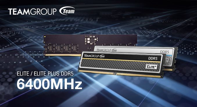
The memory kit vendor on Monday introduced its new ElitePlus-series DDR5-6400 memory modules, the first DDR5-6400 kit to be announced as JEDEC specification compliant. This means their new kit not only hits 6400 MT/s with standards-compliant timings, but arguably more importantly, it does so at DDR5's standard voltage of 1.1V as well. And while there are no platforms on the market at this time that are validated for JEDEC DDR5-6400 speeds, TeamGroup's product page already lists compatibility with Intel's yet-to-be-announced "Z790 Refresh" platform – so suitable processors seem to be due soon.
TeamGroup's Elite and ElitePlus DDR5-6400 memory modules come in 16 GB and 32 GB capacities (32 GB and 64 GB dual-channel kits) and feature JEDEC-standard CL52 52-52-103 timings as well as 1.1V voltage, as specified by the organization overseeing DRAM specs. For the moment, at least, TeamGroup's DDR5-6400 modules are the industry's fastest UDIMMs that are fully compliant with the JEDEC specifications.
And while DDR5-6400 speeds (and far higher) are available today with factory overclocked XMP/EXPO, the announcement of a JEDEC standards-compliant kit is still significant for a few different reasons. Being able to hit DDR5-6400B speeds and timings at 1.1V means DDR5 memory has improved to the point to make higher speeds at low voltages more viable, which has potential payoffs for memory at every speed grade by allowing for improved speeds and reduced power consumption/heat. And for OEM and other warrantied systems that only use JEDEC-complaint RAM, this allows for a straightforward improvement in memory speeds and bandwidth. About the only downside to faster on-spec kits is that they lack XMP or EXPO serial presence detect (SPD) profiles, which makes their configuration slightly more complicated on existing platforms from AMD and Intel, as they don't officially support DDR5-6400.
Meanwhile, on their product pages TeamGroup notes that the new RAM is compatible with Intel's "Z790 Refresh" platform, a platform that has yet to be officially announced, but is rumored to go hand-in-hand with Intel "Raptor Lake Refresh" processors. Despite the lack of formal announcements from Intel there, TeamGroup seems to have let the cat out of the bag. So, prospective owners of Z790 Refresh systems can look forward to having access to specs-compliant 1.1V DDR5-6400 memory when that platform launches later this year.
As for the modules at hand, traditionally, TeamGroup's Elite and ElitePlus memory modules are minimalistic and are aimed both at system integrators and at enthusiasts who are not after fancy designs of heat spreaders, RGB lighting, and maximum performance. In fact, TeamGroup's Elite modules do not have heat spreaders at all, whereas ElitePlus modules have a minimalistic heat spreader that will not interfere with large CPU coolers.
TeamGroup says its Elite and ElitePlus DDR5-6400 memory modules will be available separately and in dual-channel kits starting from August in North America and Taiwan. And from that, we'd assume, Raptor Lake Refresh will not be far behind.
More...
-
07-31-23, 11:12 PM #11824
Anandtech: GEEKOM AS 6 (ASUS PN53) Review: Ryzen 9 6900HX Packs Punches in a Petite P
The market demand for small form-factor (SFF) PCs was kickstarted by the Intel NUC in the early 2010s. Since then, many vendors have come out with their own take on the Intel NUC using both Intel and AMD processors. In recent years, we have also seen various Asian companies such as Beelink, Chuwi, GEEKOM, GMKtec, MinisForum, etc. emerging with a focus solely on these types of computing systems. Earlier this year, GEEKOM announced a tie-up with ASUS to market specific configurations of the ASUS ExpertCenter PN53 under their own brand as the GEEKOM AS 6. Based on AMD's Rembrandt line of notebook processors, the GEEKOM AS 6 comes with a choice of Ryzen 9 6900HX, Ryzen 7 6800H, or the Ryzen 7 7735H. Read on for a detailed look at the performance profile and value proposition of the GEEKOM AS 6's flagship configuration.
More...
-
08-01-23, 09:48 PM #11825
Anandtech: Western Digital Preps 28 TB UltraSMR Hard Drive
Western Digital is gearing up to start sampling of its 28 TB nearline hard drive for hyperscalers. The new HDD will use the company's energy-assisted perpendicular magnetic recording (ePMR) technology with UltraSMR track layouts. Since both technologies are now familiar to hyperscalers, the validation and qualification of this hard drive should be relatively straightforward.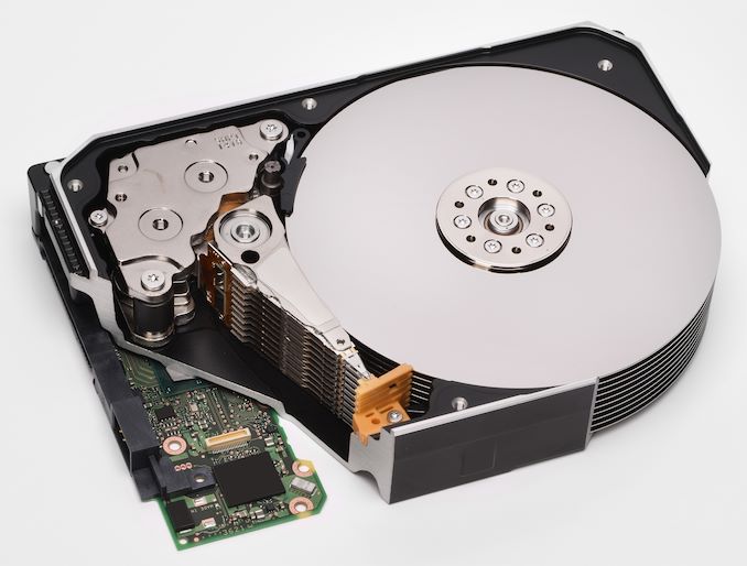
"We are about to begin product sampling of our 28 TB UltraSMR drive," said David Goeckeler, chief executive of Western Digital, at the company's most recent earnings call. "This cutting-edge product is built upon the success of our ePMR and UltraSMR technologies with features and reliability trusted by our customers worldwide. We are staging this product for quick qualification and ramp as demand improves."
Right now, Western Digital is shipping its 26 TB UltraSMR hard drives introduced over a year ago to select customers among operators of large cloud datacenters. Since these drives rely on UltraSMR it took hyperscalers quite a while to qualify them before deployment. But now that Western Digital's customers know how to use UltraSMR and what to expect from it in terms of performance and behavior, deployment of 28 TB HDDs will likely go smoother.
Based on their release timeline, Western Digital's 28 TB hard drives are expected to compete against Seagate's 32 TB HDDs based on heat-assisted magnetic recording (HAMR) technology starting early 2024. Western Digital offering will be familiar to its clients who already use shingled magnetic recording HDDs in general and UltraSMR drives in particular. Meanwhile, Seagate's product will deliver higher capacity, predictable performance (and considerably higher performance when it comes to write operations), but will probably need slightly longer qualification.
Western Digital's UltraSMR set of technologies promises to add around 20% of extra capacity to CMR (conventional magnetic recording) platters. To make UltraSMR possible, Western Digital not only had to increase the number number of shingled bands and reduce the number of CMR bands, but employ all of its leading-edge HDD technologies. This includes triple stage actuators with two-dimensional (TDMR) read heads, ePMR write heads, OptiNAND technology, Distributed Sector (DSEC) technology and a proprietary error correcting code (ECC) technology with large block encoding to ensure that increased adjacent tracks interference (ATI) does not harm data integrity. In fact, the sophisticated ECC capability supported by an HDD controller may be crucial SMR hard drives in the coming years as well as for CMR drives in the longer-term future.
One interesting thing about Western Digital's 28 TB HDD is that it will likely use the company's 2nd generation ePMR since it is based on a 24 TB CMR drive and the latter is meant to rely on the ePMR 2 technology with advanced head structures, according to Western Digital's roadmap.
More...
-
08-02-23, 08:38 AM #11826
Anandtech: ASRock Z790 Taichi Carrara Motherboard Review: ASRock Rocks With White Mar
Building on the success of their hybrid architecture Alder Lake (12th Gen) Core series chips, Intel last year released the upgraded Raptor Lake core with a similar core architecture and design with performance (P) cores and efficiency (E) cores. While we've reviewed and put Intel's 13th Gen Core series chips through their paces, it's been a while since we tested out the platforms that not only unleash that multi-threaded and single-core IPC performance but add all of the features associated with each chipset. In a series of relative socket LGA 17000 motherboard reviews, we're looking at perhaps one of the most interesting models for Intel's 13th Gen Core series.
ASRock has added 'Carrara' to the mix, adding to their already popular Taichi series of motherboards that blend cogwheel-inspired aesthetics with a premium selection of controllers and features. Sometimes referred to as Luna marble by the Romans, the ASRock Z790 Taichi Carrara edition boasts a white Carrara marble-inspired design while retaining all the exact specifications and features of the regular Z790 Taichi. Some of the most prominent features include an advertised 27-phase (24+1+2) power delivery, support for DDR5-7400 memory, as well as dual Thunderbolt 4 Type-C ports on the rear panel.
ASRock loves to be different with its offerings, aka the Aqua series of motherboards. Still, the Taichi Carrara is different in that it celebrates ASRock's 20th anniversary at the upper echelon of PC components and hardware. We take a closer look to see if the Z790 Taichi Carrara's premium standing in ASRock's Z790 line-up represents what we've come to like about the Taichi series over the years and, more importantly, how it performs against other LGA 1700 motherboards.
More...
-
08-02-23, 08:38 AM #11827
Anandtech: China Imposes New Export Restrictions on Gallium and Germanium
China this week formally imposed new export regulations on gallium and germanium, as well as materials incorporating them. This move is broadly seen as a retaliatory act for the limitations recently placed on the Chinese semiconductor industry by the U.S., Japan, and the Netherlands. These new export regulations risk eventually significantly impacting the semiconductor sector, especially factories based in Japan.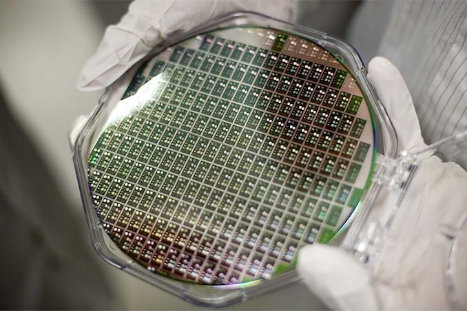
Starting from August 1, 2023, Chinese companies are required to secure an export license to export gallium and germanium metals or any products that include these elements. With a stronghold over the global production of gallium (94%) and germanium (around 60%), China's announcement of these restrictions in early July led to nearly a 20% price hike for gallium in the U.S and Europe. While the rules are said to be in the interests of China's national security, many see them as a retaliation to curbs on China's high-tech sector.
While the decision to restrict exports of gallium and germanium from China should not significantly impact the production of high-performance logic components like CPUs, GPUs, and memory, it is worth noting that GaN (gallium nitride) and GaAs (gallium arsenide) are integral to power chips, radio frequency amplifiers, LEDs, and numerous other applications.
Although gallium and germanium are not exceptionally rare and are typically acquired as byproducts of other mining operations, China's dominance in their exports is due to its cheap refinement process, which made extracting these metals in other regions financially unviable. China's new restrictions could cause an initial increase in prices and potential disruptions in supplies and component production. Yet, over time, these limitations may encourage companies from other countries to mine these metals, possibly threatening China's market dominance. For example, Pentagon recently declared plans to recover gallium from waste electronics.
Japanese companies are likely to be the most affected by these new regulations, as Japan is the largest global consumer of gallium, based on data from the Japan Organization for Metals and Energy Security. Around 60% of gallium used in the country is imported, and China contributes 70% of these imports. Consequently, approximately 40% of Japan's gallium supply is dependent on China.
Companies like Mitsubishi Chemical Group, which manufacture compound semiconductors and other products, reassure that they have adequate stocks in Japan to prevent any immediate supply issues. Other firms, including Sumitomo Chemical, a producer of gallium nitride substrates, and Nichia Corp., a producer of LEDs, also have plenty of gallium in stock, but are planning to monitor the situation and consider diversifying their suppliers. Meanwhile, to date, the new export rules have not affected Japanese companies' raw material procurement or other business operations.
Despite the new rules, China's Ministry of Commerce had stated that the export quality and quantity will remain unaffected. As long as exporters comply with national security protocols and other regulations, exports will continue as before. Meawhile, Wei Jianguo, ex-vice minister of commerce in China, cautions that the newly imposed export controls on gallium and germanium may only be the initial phase of China's countermeasures. Looking ahead, China could potentially utilize its powerful position in specific commodity markets as a strategic means for exerting economic and diplomatic influence.
Source: Nikkei
Image Source: MIT
More...
-
08-02-23, 08:02 PM #11828
Anandtech: Intel Plans Massive Expansion in Oregon: D1X and D1A to Be Upgraded
Intel has filed a permit application that outlines significant expansion plans for its campus near Hillsboro, Oregon. According to filings submitted to state regulators, the tech giant's ambitious proposals include a fourth expansion phase for the D1X research facility and an upgrade of the older D1A fab situated on the same 450-acre property.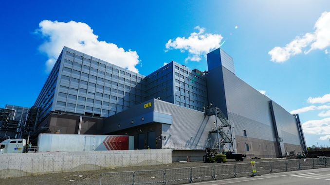
The planned enhancements will take place at the company's Gordon Moore Park (previously known as Ronler Acres) campus, according to a 1,100-page air-quality permit application submitted by Intel to the Oregon Department of Environmental Quality back in July. While the filings highlight Intel's intention to upgrade its existing facilities and build some additional capacity, they do not contain a specific financial outline for these projects. Furthermore, they indicate Intel's potential plans, not commitments. Meanwhile, if the scale is comparable to previous Oregon expansions, the total investment could reach billions.
The last upgrade, D1X's third phase, cost $3 billion and added over one million square feet to the campus. The latest expansion could potentially exceed this, given that Intel plans not only to add a fourth phase to D1X but also to overhaul the 30-year-old D1A factory, add manufacturing support buildings, and implement other upgrades. Intel anticipates that the installation of new equipment could begin as early as 2025, with the completion of additional work slated for 2028.
So far, Intel has not formally announced any plans about its Oregon campus, but in May, its chief executive Pat Gelsinger already implied that he wants the site to grow big.
"I would be reticent to constrain my dreams for how big it might be in the future," Gelsinger said.
The Gordon Moore Park site currently houses five fabs: D1X, Intel's flagship manufacturing process development facility; D1A, Intel's development fab built in the 1980s; 10nm-capable D1B and D1C fabs; and 7nm-capable D1D fab. Intel is the largest corporate employer in Oregon, with 22,000 workers.
This proposed expansion represents a significant milestone, not just for Intel but for Oregon as well. While the investment may not match the tens of billions earmarked for new campuses in Arizona and Ohio, it would nonetheless constitute one of Oregon's largest capital projects to date. This would likely result in the addition of hundreds or possibly thousands of new jobs to Intel's workforce in the state, reaffirming Intel's commitment to ongoing investment in its Oregon research endeavors.
More...
-
08-02-23, 08:02 PM #11829
Anandtech: PCI-SIG Forms Optical Workgroup - Lighting The Way To PCIe's Future
The PCI-Express interconnect standard may be going through some major changes in the coming years, based on a new announcement from the group responsible for the standard. The PCI-SIG is announcing this morning the formation of a PCIe Optical Workgroup, whose remit will be to work on enabling PCIe over optical interfaces. And while the group is still in its earliest of stages, the ramifications for the traditionally copper-bound standard could prove significant, as optical technology would bypass some increasingly stubborn limitations of copper signaling that traditional PCIe is soon approaching.
First released in the year 2000, PCI-Express was initially developed around the use of high-density edge connectors, which are still in use to this day. The PCIe Card Electromechanical specification (CEM) defines the PCIe add in card form factors in use for the last two decades, ranging from x1 to x16 connections.
But while the PCIe CEM has seen very little change over the years – in large part to ensure backward and forward compatibility – the signaling standard itself has undergone numerous speed upgrades. Including the latest PCIe 6.0 standard, the speed of a single PCIe lane has increased by 32-fold since 2000 – and the PCI-SIG will double that once more with PCIe 7.0 in 2025. As a result of increasing the amount of data transferred per pin by such a significant amount, the literal frequency band width used by the standard has increased by a similar degree, with PCIe 7.0 set to operate at nearly 32GHz.
In developing newer PCIe standards, the PCI-SIG has worked to minimize these issues, such as by employing alternative means of signaling that don’t require higher frequencies (e.g. PCIe 6 with PAM-4), and the use of mid-route retimers along with materials improvements have helped to keep up with the higher frequencies the standard does use. But the frequency limitations of copper traces within a PCB have never been eliminated entirely, which is why in more recent years the PCI-SIG has developed an official standard for PCIe over copper cabling.
Still in the works for late this year, the PCIe 5.0/6.0 cabling standard offers the option of using copper cables to carry PCIe both within a system (internal) and between systems (external). In particular, the relatively thick copper cables have less signal loss than PCB traces, overcoming the immediate drawback of high frequency comms, which is the low channel reach (i.e. short signal propagation distance). And while the cabling standard is designed to be an alternative to the PCIe CEM connector rather than a wholesale replacement, its existence underscores the problem at hand with high frequency signaling over copper, a problem that will only get even more challenging once PCIe 7.0 is made available.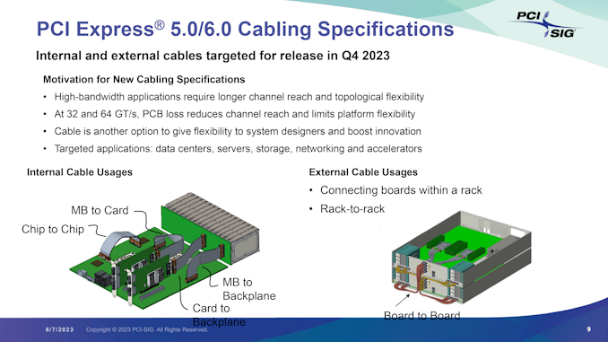
And that brings us to the formation of the PCI-SIG Optical Workgroup. Like the Ethernet community, which tends to be at the forefront of high frequency signaling innovation, PCI-SIG is looking towards optical, light-based communication as part of the future for PCIe. As we’ve already seen with optical networking technology, optical comms offers the potential for longer ranges and higher data rates vis-à-vis the vastly higher frequency of light, as well as a reduction in power consumed versus increasingly power-hungry copper transmission. For these reasons, the PCI-SIG is forming an Optical Workgroup to help develop the standards needed to supply PCIe over optical connections.
Strictly speaking, the creation of a new optical standard isn’t necessary to drive PCIe over optical connections. Several vendors already offer proprietary solutions, with a focus on external connectivity. But the creation of an optical standard aims to do just that – standardize how PCIe over fiber optics would work and behave. As part of the working group announcement, the traditionally consensus-based PCI-SIG is making it clear that they aren’t developing a standard for any single optical technology, but rather they are aiming to make it technology-agnostic, allowing the spec to support a wide range of optical technologies.
But the relatively broad announcement from the PCI-SIG doesn’t just stop with optical cabling as a replacement for current copper cabling, the group is also looking at “potentially developing technology-specific form factors.” While the classic CEM connector is unlikely to go away entirely any time soon – the backwards and forwards compatibility is that important – the CEM connector is the weakest/most difficult way to deliver PCIe today. So if the PCI-SIG is thinking about new form factors, then it’s likely the Optical Workgroup will at least be looking at some kind of optical-based successor to the CEM. And if that were to come to pass, this would easily be the biggest change in the PCIe specification in its 23+ year history.
But, to be sure, if any such change were to happen, it would be years down the line. The new Optical Workgroup has yet to form, let alone set its goals and requirements. With a broad remit to make PCIe more optical-friendly, any impact from the group is several years away – presumably no sooner than making a cabling standard for PCIe 7.0, if not a more direct impact on a PCIe 8.0 specification. But it shows where PCI-SIG leadership sees the future of the PCIe standard going, assuming they can get a consensus from their members. And, while not explicated stated in the PCI-SIG’s press release, any serious use of optical PCIe in this fashion would seem to be predicated on cheap optical transceivers, i.e. silicon photonics.
In any case, it will be interesting to see what eventually comes out of the PCI-SIG’s new Optical Workgroup. As PCIe begins to approach the practical limits of copper, the future of the industry’s standard peripheral interconnect may very well be to go towards the light.
More...
-
08-03-23, 09:11 AM #11830
Anandtech: AMD Announces Radeon Pro W7600 & W7500: Pro RDNA 3 For The Mid-Range
As AMD continues to launch their full graphics product stacks based on their latest RDNA 3 architecture GPUs, the company is now preparing their next wave of professional cards under the Radeon Pro lineup. Following the launch of their high-end Radeon Pro W7900 and W7800 graphics cards back in the second quarter of this year, today the company is announcing the low-to-mid-range members of the Radeon Pro W7000 series: the Radeon Pro W7500 and Radeon Pro W7600. Both based on AMD’s monolithic Navi 33 silicon, the latest Radeon Pro parts will hit the shelves a bit later this quarter.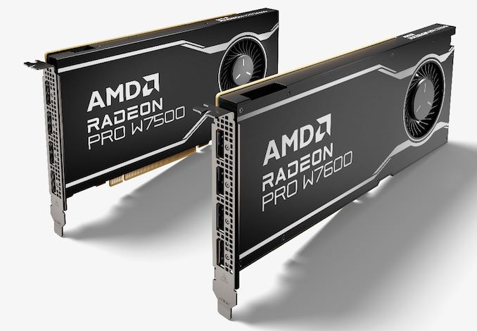
The two cards, as a whole, will make up what AMD defines as the mid-range segment of their professional video card market. And like their flagship counterparts, AMD is counting on a combination of RDNA 3’s advanced features, including AV1 encoding support, improved compute and ray tracing throughput, and DisplayPort 2.1 outputs to help drive sales of the new video cards. That, and as is tradition, significantly undercutting NVIDIA’s competing professional cards.
More...


 Quote
Quote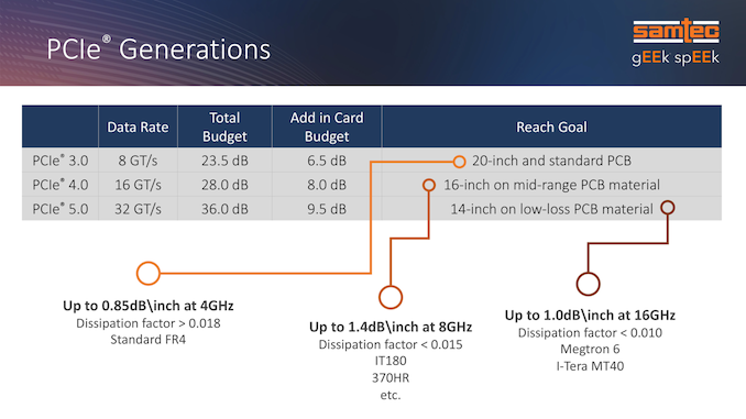
Thread Information
Users Browsing this Thread
There are currently 37 users browsing this thread. (0 members and 37 guests)


Bookmarks