

Results 11,901 to 11,910 of 12091
Thread: Anandtech News
-
09-28-23, 04:32 PM #11901
Anandtech: Intel Meteor Lake SoC is NOT Coming to Desktops: Well, Not Technically
Over the last couple of days, numerous reports have revealed that Intel's recently announced Meteor Lake SoC, primarily a mobile platform, would be coming to desktop PCs. Intel has further clarified that while their Meteor Lake processors will be featured in desktop systems next year, they won't power traditional socketed desktop PCs. Instead, these CPUs, primarily crafted for laptops, will be packaged in ball grid array (BGA) formats, making them suitable for compact desktops and all-in-one (AIO) devices.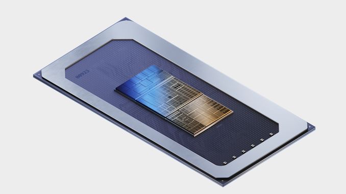
Intel's statement, as reported by ComputerBase, emphasizes, "Meteor Lake is a power efficient architecture that will power innovative mobile and desktop designs, including desktop form factors such as All-in-One (AIO). We will have more product details to share in the future."
A senior Intel official recently mentioned that Meteor Lake processors are slated for desktop release in 2024. However, they won't be available in Intel's LGA1851 form factor, which caters to gaming rigs, client workstations, and conventional desktop systems. The practice of integrating laptop CPUs into compact PCs, such as NUCs and all-in-one PCs, isn't a novel one. Manufacturers have been doing this for years, and the intriguing aspect will be observing the performance and efficiency metrics of these high-end Meteor Lake laptop CPUs, especially when juxtaposed against the existing Raptor Lake processors designed for both desktops and laptops.
The rationale behind Intel's decision to exclude Meteor Lake processors from socketed desktops remains ambiguous. The CPU employs a multi-tile structure, with its compute tile being developed on the Intel 4 process technology. This technology marks Intel's inaugural use of extreme ultraviolet lithography (EUV), while the graphics tile and SoC leverage TSMC's fabrication methods. Both production techniques are poised to deliver commendable performance and efficiency, but Meteor Lake is not designed as a pure desktop product.
Current indications suggest that the Arrow Lake-S series will be aimed at LGA1851 motherboards, but this is anticipated for the latter half of 2024. While Q3/Q4 of 2024 is still a while away, Intel's motherboard partners, such as GIGABYTE and MSI, have been readying up new refreshed Z790 motherboards, with features such as Wi-Fi 7 set to come to Intel's impending Raptor Lake refresh platform which is due sometime before the end of the year.
Source: ComputerBase
More...
-
09-29-23, 11:19 AM #11902
Anandtech: Micron to Ship HBM3E Memory to NVIDIA in Early 2024
Micron has reaffirmed plans to start shipments of its HBM3E memory in high volume in early 2024, while also revealing that NVIDIA is one of its primary customers for the new RAM. Meanwhile, the company stressed that its new product has been received with great interest by the industry at large, hinting that NVIDIA will likely not be the only customer to end up using Micron's HBM3E.
"The introduction of our HBM3E product offering has been met with strong customer interest and enthusiasm," said Sanjay Mehrotra, president and chief executive of Micron, at the company's earnings call.
Introducing HBM3E, which the company also calls HBM3 Gen2, ahead of its rivals Samsung and SK Hynix is a big deal for Micron, which is an underdog on the HBM market with a 10% market share. The company obviously pins a lot of hopes on its HBM3E since this will likely enable it to offer a premium product (to drive up its revenue and margins) ahead of its rivals (to win market share).
Typically, memory makers tend not to reveal names of their customers, but this time around Micron emphasized that its HBM3E is a part of its customer's roadmap, and specifically mentioned NVIDIA as its ally. Meanwhile, the only HBM3E-supporting product that NVIDIA has announced so far is its Grace Hopper GH200 compute platform, which features an H100 compute GPU and a Grace CPU.
"We have been working closely with our customers throughout the development process and are becoming a closely integrated partner in their AI roadmaps," said Mehrotra. "Micron HBM3E is currently in qualification for NVIDIA compute products, which will drive HBM3E-powered AI solutions."
Micron's 24 GB HBM3E modules are based on eight stacked 24Gbit memory dies made using the company's 1β (1-beta) fabrication process. These modules can hit date rates as high as 9.2 GT/second, enabling a peak bandwidth of 1.2 TB/s per stack, which is a 44% increase over the fastest HBM3 modules available. Meanwhile, the company is not going to stop with its 8-Hi 24 Gbit-based HBM3E assemblies. The company has announced plans to launch superior capacity 36 GB 12-Hi HBM3E stacks in 2024 after it initiates mass production of 8-Hi 24GB stacks.
"We expect to begin the production ramp of HBM3E in early calendar 2024 and to achieve meaningful revenues in fiscal 2024," added chief executive of Micron.
More...
-
10-02-23, 03:04 PM #11903
Anandtech: Asus Formally Completes Acquisition of Intel's NUC Business
ASUS has formally acquired Intel's Next Unit of Computing (NUC) products based on Intel's 10th to 13th Generation Core processors. Asus is set to continue building and supporting Intel's existing NUCs and will, over time, roll out its own compact NUC systems for office, entertainment, gaming, and many other applications.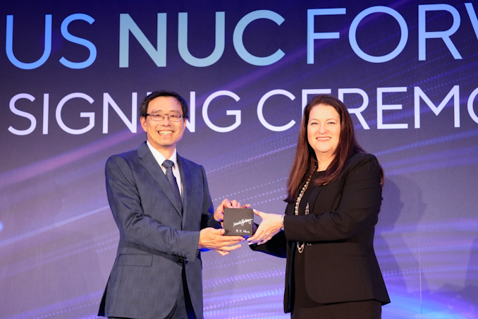
"I am confident that this collaboration will enhance and accelerate our vision for the mini PC," said Jackie Hsu, Asus senior vice president and co-head of OP & AIoT business groups, at the signing ceremony. "Adding the Intel NUC product line to our portfolio will extend ASUS's AI and IoT R&D capabilities and technology solutions, especially in three key markets – industrial, commercial, and prosumer."
Asus held a formal handover ceremony in Taipei and took control of the NUC product lines that span from business applications to gaming. With the acquisition, Asus instantly commenced business processes for the NUC range, ensuring a hassle-free transition for existing customers. Under the terms of the agreement, Asus obtained licenses for both Intel's hardware designs and software. This move widens Asus's operational scope in R&D and extends its reach in logistics, tech support, and numerous application areas.
Asus envisions broadening its NUC product line and distribution channels. The focus will remain on offering high-quality compact PCs with robust security and advanced technologies, which NUC is known for. ASUS also aims to produce eco-friendly NUC products while emphasizing impeccable service for its customer base.
"This is an exciting time for both Intel and Asus as we move forward with the next chapter in NUC's story," said Michelle Johnston Holthaus, Executive Vice President and General Manager of the Client Computing Group at Intel, who also attended the event. "Today's signing ceremony signifies more than just a business deal. It signifies ASUS' dedication to enhancing the lives of NUC customers and partners around the world. I look forward to seeing NUC thrive as part of the ASUS family."
It should be noted that Asus's Intel NUC license is not exclusive, so Intel may eventually enable other PC makers to build its NUCs and, therefore, compete against Apple.
Source: Asus
More...
-
10-03-23, 10:02 AM #11904
Anandtech: Tenstorrent to Use Samsungs SF4X for Quasar Low-Cost AI Chiplet
Tenstorrent this week announced that it had chosen to use Samsung's SF4X (4 nm-class) process technology for its upcoming low-cost, low-power codenamed Quasar chiplet for machine learning workloads. The chiplets will be made at Samsung's new fab near Taylor, Texas when it becomes operational in 2024.
Tenstorrent's Quasar chiplet is a new addition to the company's roadmap. Based on an image provided by the company, the chiplet is set to pack at least 80 Tensix cores based on the RISC-V instruction set architecture and tailored to run artificial intelligence workloads in a variety of formats, such as BF4, BF8, INT8, FP16, and BF16. Tenstorrent's Quasar's are designed to operate in groups and be paired with the company's CPU chiplets, so they are equipped with non-blocking die-to-die interfaces.
Samsung's SF4X is a process technology designed for high-performance computing applications. It is tailored for high clocks and high voltages to ensure maximum performance.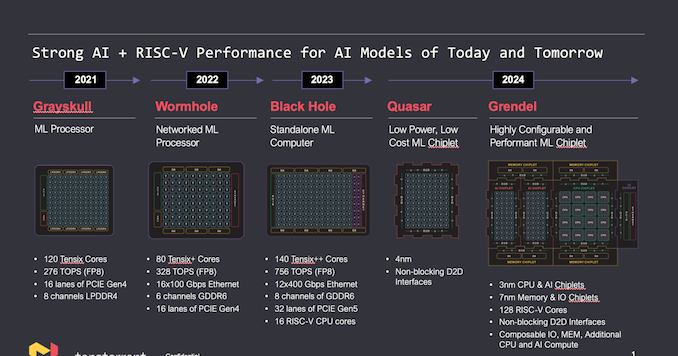
Tenstorrent does not disclose the estimated performance of its Quasar chiplet, but assuming that it has 80 Tensix cores, which is the same number as the Wormhole chiplet taking a 328 FP8 TOPS performance, we can probably make a similar estimate of the performance, considering that it is made using a performance-enhanced process technology.
Tenstorrent officially positions its Quasar chiplets as a low-power, low-cost solution for machine learning, so we can only wonder whether the company will try to squeeze every last bit of performance out of them or choose a different power strategy.
"Samsung Foundry is expanding in the U.S., and we are committed to serving our customers with the best available semiconductor technology," said Marco Chisari, head of Samsung's U.S. Foundry business. "Samsung's advanced silicon manufacturing nodes will accelerate Tenstorrent's innovations in RISC-V and AI for data center and automotive solutions. We look forward to working together and serving as Tenstorrent's foundry partner."
One interesting wrinkle about Tenstorrent's relationship with Samsung is that it recently secured $100 million in financing from various companies in a round co-led by Hyundai Motor Group and the Samsung Catalyst Fund. Hyundai and Samsung need AI processors in one form or another, so it is not surprising that their funds are invested in Tenstorrent. Meanwhile, and I am speculating here, the same applies to chipmaking, and Samsung may be interested in producing chips for Tenstorrent for strategic reasons.
Gallery: Tenstorrent to Use Samsungs SF4X for Quasar Low-Cost AI Chiplet

More...
-
10-03-23, 10:02 AM #11905
Anandtech: Samsung T9 Portable SSD Review: A 20 Gbps PSSD for Prosumer Workloads
Samsung's portable SSD lineup has enjoyed significant market success since the launch of the T1 back in 2015. Despite the release of the Thunderbolt-capable X5 PSSD in 2018, the company has been focusing on the mainstream market. Multiple T series drives have made it to the market over the last 8 years. The product line made the transition to NVMe and USB 3.2 Gen 2 only in 2020 with the launch of the T7 Touch. Today, the company unveiled its first USB 3.2 Gen 2x2 (20 Gbps) PSSD - the Samsung T9. Read on for an in-depth investigation into the design and performance profile of the T9's 4 TB version.
More...
-
10-03-23, 03:31 PM #11906
Anandtech: Seagate Releases Game Drive PCIe 4.0 SSDs for PlayStation 5
Western Digital's WD_Black SN850P was the first officially PlayStation 5-licensed SSD to hit the market. Seagate wants a piece of that and has hopped on the PlayStation 5 train with the new Game Drive PCIe 4.0 NVMe SSD series, officially licensed for Sony's current-generation gaming console.
Unlike Microsoft, which uses a proprietary SSD expansion card for the Xbox Series X and Xbox Series S, Sony opted to employ a standard M.2 slot for storage expansion on the PlayStation 5. The Japanese console maker's decision provides more storage options for gamers since they have many M.2 SSD offerings on the market. The M.2 slot has also paved the way for SSD manufacturers to partner with Sony to release licensed drives, which have been tested and approved for the PlayStation 5. Therefore, you don't want to worry whether the SSD's heatsink keeps the drive cool or if the Game Drive will fit inside the PlayStation 5.
Seagate's Game Drive SSDs, like the WD_Black SN850P, stick to the PCIe 4.0 x4 interface. That's the same interface in the PlayStation 5, so it makes little sense for vendors to tailor faster toward the gaming console. The Game Drive SSDs utilize Phison's PS5018-E18 PCIe 4.0 SSD controller capable of hitting write and read speeds over 7 GB/s. Built with TSMC's 12nm process node, the E18 is a popular, high-end SSD controller for mainstream PCIe 4.0 SSDs. The E18 comes equipped with three 32-bit Arm Cortex R5 CPU cores and an eight-channel design to support NAND flash speeds up to 1,600 MT/s and capacities up to 8 TB. Seagate pairs the E18 controller with unspecified 3D TLC NAND in the company's Game Drive SSDs.
[TABLE="align: center"]
[TR="class: tgrey"]
[TD="colspan: 4, align: center"]Seagate Game Drive Specifications[/TD]
[/TR]
[TR="class: tlblue"]
[TD] [/TD]
[TD="align: center"]1 TB[/TD]
[TD="align: center"]2 TB[/TD]
[TD="align: center"]4 TB[/TD]
[/TR]
[TR]
[/TR]
[TR]
[TD="class: tlgrey"]Part Number[/TD]
[TD="align: center"]ZP1000GP304001[/TD]
[TD="align: center"]ZP2000GP304001[/TD]
[TD="align: center"]ZP4000GP304001[/TD]
[/TR]
[TR]
[TD="class: tlgrey"]Seq Reads (MB/s)[/TD]
[TD="align: center"]7,300[/TD]
[TD="align: center"]7,300[/TD]
[TD="align: center"]7,250[/TD]
[/TR]
[TR]
[TD="class: tlgrey"]Seq Writes (MB/s)[/TD]
[TD="align: center"]6,000[/TD]
[TD="align: center"]6,900[/TD]
[TD="align: center"]6,900[/TD]
[/TR]
[TR]
[TD="class: tlgrey"]Random Reads (K IOPS)[/TD]
[TD="align: center"]800[/TD]
[TD="align: center"]1,000[/TD]
[TD="align: center"]1,000[/TD]
[/TR]
[TR]
[TD="class: tlgrey"]Random Writes (K IOPS)[/TD]
[TD="align: center"]1,000[/TD]
[TD="align: center"]1,000[/TD]
[TD="align: center"]1,000[/TD]
[/TR]
[TR]
[TD="class: tlgrey"]Endurance (TBW)[/TD]
[TD="align: center"]1,275[/TD]
[TD="align: center"]2,550[/TD]
[TD="align: center"]5,100[/TD]
[/TR]
[TR]
[TD="class: tlgrey"]Active Power, Average (W)[/TD]
[TD="align: center"]6.3[/TD]
[TD="align: center"]7.8[/TD]
[TD="align: center"]8.6[/TD]
[/TR]
[TR]
[TD="class: tlgrey"]Idle Power PS3, Average (mW)[/TD]
[TD="align: center"]20[/TD]
[TD="align: center"]25[/TD]
[TD="align: center"]30[/TD]
[/TR]
[TR]
[TD="class: tlgrey"]Low Power L1.2 mode (mW)[/TD]
[TD="align: center"]
-
10-04-23, 02:31 PM #11907
Anandtech: Intel to Spin-off Programmable Solutions Group as Standalone Business, Eye
Intel this afternoon has announced that the company will be spinning off its programmable solutions group (PSG), to operate as a standalone business. The business unit, responsible for developing Intel’s Agilex, Stratix, and other FPGA products, will become a standalone entity under Intel’s corporate umbrella starting in Q1 of 2024, with the long-term goal of eventually selling off part of the group in an IPO in two to three years’ time.
The reorganization announced today will see Intel’s PSG transition to operating as a standalone business unit at the start of 2024, with Intel EVP Sandra Rivera heading up PSG as its new CEO. Rivera is currently the general manager of Intel’s Data Center and AI Group (DCAI), which is where PSG is currently housed, so she has significant familiarity with the group. In the interim, Rivera will also continue serving in her role in DCAI until Intel can find a replacement, with the company looking for candidates both externally and internally.
The separating of PSG is the latest move from Intel to reorganize the company’s multi-faceted business in an effort to focus on its core competencies of silicon photolithography and chip design. Since bringing on current CEO Pat Gelsinger two years ago, Intel has sold or spun off several business units, including its SSD business, NUC mini-PC business, Mobileye ADAS unit, and others, all the while making significant new investments in Intel’s Foundry Services (IFS) fab division. Though, unlike some of Intel's other divestments, it's notable that the company isn't separating from PSG because the business unit is underperforming or is in a commoditized, low-margin market – rather, Intel thinks PSG could perform even better without the immense business and bureaucratic weight of Intel hanging over it.
For the standalone PSG business unit, Intel is eyeing a very similar track to how they’ve handled Mobileye, which will see Intel maintaining majority ownership while still freeing up the business unit to operate more independently. This strategy has played out very well for Mobileye, with the company enjoying continued commercial growth while successfully IPOing last year, and which Intel is hoping they can achieve again with a standalone PSG.
This business unit separation comes as Intel, by their own admittance, has mismanaged PSG. While PSG has enjoyed a string of record quarters financially, Intel believes that PSG has been underserving the true high growth, high profitability markets for FPGAs, such as industrial, automotive, defense, and aerospace. Since being acquired by Intel in 2015 – and especially in the last few years as a formal part of DCAI – Intel’s PSG has been focused on datacenter solutions, to the detriment of other business segments.
Reforming PSG as a standalone business unit, in turn, is intended to improve the agility of the business unit. While PSG will remain under the ownership of Intel both now and in the future, Intel’s control over the group will be largely reduced to that of an investor. This will leave Sandra Rivera and her leadership team free to adjust the company’s product portfolio and positioning as to best serve the wider FPGA market, and not just Intel’s datacenter-centric ambitions. Meanwhile, if all goes well, over the long-haul Intel gets to pocket the profits of a successful IPO while having one less business unit to manage, allowing Intel to funnel its money and time into its own higher priority ventures such as fabs.
Keeping in mind that the PSG was an acquisition for Intel in the first place, in some respects this is an unwinding of that acquisition. In 2015 Intel paid $16.7 billion for what was then Altera, which under Intel became the PSG as we know it today. And while Intel’s eventual IPO plans for PSG have them retaining a stake in the business unit – and a majority stake, at that – this very much re-separates PSG/Altera in terms of operations.
Still, PSG/Altera has a very long history with Intel, going all the way back to 1984, and even as a standalone business unit, PSG will still be tied closely to Intel. Altera will be free to use whatever contract fab it would like, but as the company has been under Intel’s umbrella all this time, it is no surprise that many of the company’s upcoming products are slated to be built at Intel’s fabs, where PSG is expecting to leverage Intel’s advanced packaging techniques. And over the longer term, as Intel lays the groundwork to become the top contract fab in the world, it’s Intel’s hope that they’ll be able to keep PSG’s business.
At the same time, however, PSG will need to win back the business it has lost in the last several years due to its datecenter focus under Intel. The FPGA space is highly competitive, with arch rival AMD having acquired Xilinx in 2020, and who is starting to reap some of the first benefits of that acquisition and integration. Meanwhile in the low power FPGA space, fellow Oregon firm Lattice Semiconductor is not to be underestimated. Intel believes the FPGA market is primed for significant growth – on the order of a “high single digit” compound annual growth rate – so it’s not just a matter of winning back existing dollars from PSG’s rivals. But they’ll have to win back mindshare as well, a task that may take a significant amount of time as the FPGA market moves much slower and offers much longer-lived products than the CPU market.
But first, PSG must get ready to stand on its own two feet. PSG will transition to operating as a standalone business unit at the start of 2024, and it will be reported as such on Intel’s financial statements. Meanwhile, Intel is looking to bring on an initial external investor in 2024, to act as an outside resource to help prepare the group for an eventual IPO. According to Intel, PSG will need two to three years to develop the financial history and leadership stability for a successful IPO, which is why Intel is focusing on making the business unit standalone now, while eyeing an IPO a few years down the line.
Finally, for now it remains to be seen what the standalone PSG will be calling itself. As “programmable solutions group” is arguably unsuitable as a business name, expect to see PSG renamed. Whether that means resurrecting the Altera name or coming up with a new name entirely, as part of standing up on its own two feet, Intel’s FPGA business will need an identity of its own to become a business of its own.
More...
-
10-06-23, 02:24 PM #11908
Anandtech: ASRock Industrial NUC BOX-N97 and GMKtec NucBox G2 Review: Contrasting Com
Intel has been maintaining a low-power / low-cost x86 microarchitecture since the introduction of the Silverthorne Atom processors in 2008. Its latest iteration, Gracemont, made its debut in the Alder Lake lineup. The hybrid processors in that family teamed up the Gracemont efficiency cores with the Golden Cove performance cores. Eventually, Intel released a new line of processors under the 'Alder Lake-N' (ADL-N) tag comprising only the Gracemont cores. As a replacement for the Tremont-based Jasper Lake SoCs, ADL-N has found its way into a variety of entry-level computing systems including notebooks and compact desktops.
ASRock Industrial's lineup of ultra-compact form-factor (UCFF) systems - the Intel-based NUC BOX series and AMD-based 4X4 BOX series - has enjoyed significant market success. At the same time, the expanding market for compact computing systems has also brought many Asian manufacturers such as ACEMAGIC, Beelink, GMKtec, and MinisForum into play. As ADL-N ramps up, we are seeing a flood of systems based on it from these vendors. We took advantage of this opportunity to source two contrasting ADL-N mini-PCs - the ASRock Industrial NUC BOX-N97 and the GMKtec NucBox G2. Though both systems utilize a quad-core ADL-N SoC, the feature set and target markets are very different. Read on for a detailed analysis of the system features, build, performance profile, and value proposition of the NUC BOX-N97 and the NucBox G2.
More...
-
10-11-23, 02:46 AM #11909
Anandtech: Intel Launches Arc A580: A $179 Graphics Card for 1080p Gaming
When Intel unveiled its range of Arc A-series desktop graphics cards last year, it introduced four models: the Arc A770, Arc A750, Arc A580, and Arc A380. However, the Arc A580, which uses a cut-down ACM-G10 GPU, never reached the market for reasons that remain unclear. On Tuesday Intel finally fleshed out the Arc desktop lineup with a 500 series card, formally and immediately launching the Arc A580 graphics card.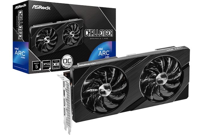
Intel's Arc A580 is based on the Alchemist ACM-G10 graphics processor with 3072 stream processors and that is paired with 8 GB of memory using a 256-bit interface. While the the cut-down GPU has fewer SPs than its higher-performing counterparts, it retains all of the features that the Alchemist architecture has to offer, including world-class media playback capabilities, including hardware accelerated decoding and encoding in AV1, H.264, and H.265 formats.
The card sits under the Arc A770 and Arc A750 in terms of performance, but above the Arc A380, thus targeting gamers in budget. Intel itself positions its Arc A580 for 1080p gaming against AMD's Radeon RX 6600 and NVIDIA's GeForce RTX 3050 graphics cards that have been available on the market for about two-and-a-half years.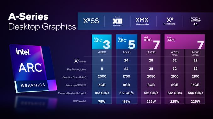
When compared to its rivals, the Arc A580 has higher compute performance (10.445 FP32 TFLOPS vs. Radeon RX 6600's 9 FP32 TFLOPS and GeForce RTX 3050's 8 FP32 TFLOPS) as well as dramatically higher memory bandwidth (512 GB/s vs. 224 GB/s). Though as FLOPS are not everything, we'll have to see how benchmarks play out. The biggest advantage for Intel right now is going to be memory bandwidth, as Intel is shipping a card with a far wider memory bus than anything else in this class – something that AMD and NVIDIA shied away from after multiple cryptocurrency rushes and crashes.
But Intel's Arc A580 is more power hungry than its rivals: as this part is based on Intel's top-tier ACM-G10 GPU, it has the power consumption to match, with a total graphics power rating of 185W. Conversely, AMD's Radeon RX 6600 and NVIDIA's GeForce RTX 3050 are rated for 132W and 130W, respectively.
Graphics cards based on the Intel Arc A580 GPU are set to be offered by ASRock, Gunnir, and Sparkle, starting at $179. At $179, the boards are cheaper than AMD's Radeon RX 6600 ($199) and Nvidia's GeForce RTX 3050 ($199), which makes it quite a competitive offering. Meanwhile, Intel's higher-performing Arc A750 can now be obtained for $189 - $199, which somewhat reduces appeal of the new board – though it remains to be seen if those A750 prices will last.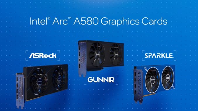
More...
-
10-12-23, 07:06 PM #11910
Anandtech: TSMC: Ecosystem for 2nm Chip Development Is Nearing Completion
Speaking to partners last week as part of their annual Open Innovation Platform forum in Europe, a big portion of TSMC's roadshow was dedicated to the next generation of the company's foundry technology. TSMC's 2 nm-class N2, N2P, and N2X process technologies are set to introduce multiple innovations, including nanosheet gate-all-around (GAA) transistors, backside power delivery, and super-high-performance metal-insulator-metal (SHPMIM) capacitor over the next few years. But in order to take advantage of these innovations, TSMC warns, chip designers will need to use all-new electronic design automation (EDA), simulation, and verification tools as well as IP. And while making such a big shift is never an easy task, TSMC is bringing some good news to chip designers early-on: even with N2 still a couple of years out, many of the major EDA tools, verification tools, foundation IP, and even analog IP for N2 are already available for use.
"For N2 we could be working with them two years in advance already because nanosheet is different," said Dan Kochpatcharin, Head of Design Infrastructure Management at TSMC, at the OIP 2023 conference in Amsterdam. "[EDA] tools have to be ready, so what the OIP did is to work with them early. We have a huge engineering team to work with the EDA partners, IP partners, [and other] partners."
*Chip density published by TSMC reflects 'mixed' chip density consisting of 50% logic, 30% SRAM, and 20% analog.Advertised PPA Improvements of New Process Technologies
Data announced during conference calls, events, press briefings and press releasesTSMC N5
vs
N7N3
vs
N5N3E
vs
N5N2
vs
N3EPower -30% -25-30% -34% -25-30% Performance +15% +10-15% +18% +10-15% Chip Density* ? ? ~1.3X >1.15X Volume
ManufacturingQ2 2022 H2 2022 Q2/Q3 2023 H2 2025
Preparations for the start of N2 chip production, scheduled for sometime in the second half of 2025, began long ago. Nanosheet GAA transistors behave differently than familiar FinFETs, so EDA and other tool and IP makers had to build their products from scratch. This is where TSMC's Open Innovation Platform (OIP) demonstrated its prowess and enabled TSMC's partners to start working on their products well in advance.
By now, major EDA tools from Cadence and Synopsys as well as many tools from Ansys and Siemens EDA have been certified by TSMC, so chip developers can already use them to design chips. Also, EDA software programs from Cadence and Synopsys are ready for analog design migration. Furthermore, Cadence's EDA tools already support N2P's backside power delivery network.
With pre-built IP designs, things are taking a bit longer. TSMC's foundation libraries and IP, including standard cells, GPIO/ESD, PLL, SRAM, and ROM are ready both for mobile and high-performance computing applications. Meanwhile, some PLLs exist in pre-silicon development kits, whereas others are silicon proven. Finally, blocks such as non-volatile memory, interface IP, and even chiplet IP are not yet available - bottlenecking some chip designs - but these blocks in active development or planned for development by companies like Alphawave, Cadence, Credo, eMemory, GUC, and Synopsys, according to a TSMC slide. Ultimately, the ecosystem of tools and libraries for designing 2 nm chips is coming together, but it's not all there quite yet.
"[Developing IP featuring nanosheet transistors] is not harder, but it does take more cycle time, cycle time is a bit longer," said Kochpatcharin. "Some of these IP vendors also need to be trained [because] it is just different. To go from planar [transistor] to FinFET, is not harder, you just need to know how to do the FinFET. [It is] same thing, you just need to know how to do [this]. So, it does take some to be trained, but [when you are trained], it is easy. So that is why we started early."
Although many of the major building blocks for chips are N2-ready, a lot of work still has to be done by many companies before TSMC's 2 nm-class process technologies go into mass production. Large companies, which tend to design (or co-design) IP and development tools themselves are already working on their 2 nm chips, and should be ready with their products by the time mass production starts in 2H 2025. Other players can also fire up their design engines because 2 nm preps are well underway at TSMC and its partners.
More...


 Quote
QuoteThread Information
Users Browsing this Thread
There are currently 21 users browsing this thread. (0 members and 21 guests)


Bookmarks