

Results 11,911 to 11,920 of 12091
Thread: Anandtech News
-
10-12-23, 07:06 PM #11911
Anandtech: Samsung Lines Up First Server Customer For 3nm Fabs
Although Samsung Foundry was the first contract fab to formally start mass production of chips on a 3 nm-class process, so far, the company's latest process has largely been relegated to producing tiny cryptocurrency mining chips. But it looks like things will start picking up for Samsung's foundry business soon, as this week it was announced that the company has landed a more substantial order which will see the Samsung make a server-grade system-in-package (SiP) with HBM memory for an unknown client.
Per this week's press releases, Samsung Foundry is set to produce a server-grade processor with HBM memory that is set to be designed by ADTechnology, a contract chip developer from South Korea, for an American company. For now, details on the chip are light, so all we know about the 3 nm-based datacenter product is that it will will use 2.5D packaging in conjunction with HBM memory. All of which points to a high-end system-on-chip (SoC) – or rather a system-in-package (SiP).
"This 3nm project will be one of the largest semiconductor products in the industry," said Park Joon-Gyu, chief executive of AD Technology. "This 3nm and 2.5D design experience will be a significant differentiation factor between other companies and AD Technology. We will do our utmost to deliver the best design results to our customers."
Meanwhile, it is unclear which of Samsung Foundry's 3 nm-class process technologies the company is set to use for the project. Currently the company is producing cryptocurrency mining ASICs using its SF3E process technology, which is the initial version of Samsung's gate-all-around (GAA) manufacturing tech.
The company is set to roll-out an enhanced SF3 process technology next year. This version of the node provides additional design flexibility, which is enabled by varying nanosheet channel widths of the GAA device within the same cell type. All of this will, in turn, improve the performance, power, and area characteristics of SF3 compared to SF3E, making it more suitable for server designs. Yet, the company is also prepping SP3P technology with performance enhancements for 2025, which is likely to be even better for server-grade silicon.
"We are pleased to announce our 3nm design collaboration with AD Technology," said Jung Ki-Bong, Vice President of Samsung Electronics Foundry Business Development team. "This project will set a good precedent in the collaboration program between Samsung Electronics Foundry Division and our ecosystem partners, and Samsung Electronics Foundry Division will strengthen our cooperation with partners to provide the best quality to our customers."
Sources: ADTechnology, Pulsenew
More...
-
10-16-23, 11:02 PM #11912
Anandtech: Intel Announces 14th Gen Core Series For Desktop: Core i9-14900K, Core i7-
Ahead of tomorrow's full-scale launch, Intel this afternoon is pre-announcing their 14th Generation Core desktop processors. Aptly codenamed Raptor Lake Refresh, these new chips are based on Intel's existing Raptor Lake silicon – which was used in their 13th generation chips – with Intel tapping further refinements in manufacturing and binning in order to squeeze out a little more performance from the silicon. For their second iteration of Raptor Lake, Intel is also preserving their pricing for the Core i9, i7, and i5 processors, which aligns with the pricing during the launch of Intel's 13th Gen Core series last year.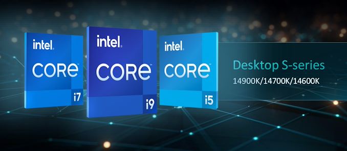
Headlining the new lineup is Intel's latest flagship desktop processor, the Core i9-14900K, which can boost up to 6 GHz out of the box. This is the second Intel Raptor Lake chip to hit that clockspeed – behind their special edition Core i9-13900KS – but while that was a limited edition chip, the Core i9-14900K is Intel's first mass-produced processor that's rated to hit 6 GHz. Under the hood, the i9-14900K uses the same CPU core configuration as the previous Core i9-13900K chips, with 8 Raptor Cove performance (P) cores and 16 Gracemont-based efficiency (E) cores, for a total of 24 CPU cores capable of executing on 32 threads.
Moving down the stack, arguably the most interesting of the chips being announced today is the new i7-tier chip, the Core i7-14700K. Intel's decision to bolster the core count of its Core i7 is noteworthy: the i7-14700K now boasts 12 E-cores and 8 P-cores, 4 more E-cores than its 13th Gen counterpart – and only 4 behind the flagship i9. With base clock rates mirroring the previous generation's Core i7-13700K, the additional efficiency cores aim to add extra range in multitasking capabilities, designed to benefit creators and gamers.Intel 14th Gen Core, Raptor Lake-R (K/KF Series)
Pricing as of 10/16AnandTech Cores
P+E/TP-Core
BaseP-Core
TurboE-Core
BaseE-Core
TurboL3 Cache
(MB)iGPU Base
WTurbo
WPrice
($)i9-14900K 8+16/32 3200 6000 2400 4400 36 770 125 253 $589 i9-14900KF 8+16/32 3200 6000 2400 4400 36 - 125 253 $564 i9-13900K 8+16/32 3000 5800 2200 4300 36 770 125 253 $537 i7-14700K 8+12/28 3400 5600 2500 4300 30 770 125 253 $409 i7-14700KF 8+12/28 3400 5600 2500 4300 30 - 125 253 $384 i7-13700K 8+8/24 3400 5400 2500 4200 30 770 125 253 $365 i5-14600K 6+8/20 3500 5300 2600 4000 24 770 125 181 $319 i5-14600KF 6+8/20 3500 5300 2600 4000 24 - 125 181 $294 i5-13600K 6+8/20 3500 5300 2600 3900 24 770 125 181 $285
Rounding out the 14th Gen Core collection is the i5 series. Not much has changed between the latest Core i5-14600K and the Core i5-13600K, with the only differences coming in E-core turbo frequencies; just a 100 MHz uptick here. Both families share the same 6P+8E (20T) configuration, 5.3 GHz P-core turbo, and 3.5 GHz P-core base frequencies. Price-wise (at the time of writing), the Core i5-13600K is currently available at Amazon for $285, which is a $34 saving over the MSRP of the Core i5-14600K, and that money could potentially be spent elsewhere, such as storage or memory.
Since the Intel 14th and 13th Gen core series are essentially the same chips but with slightly faster frequencies, Intel has made no changes to the underlying core architecture. Intel does include a new overclocking feature for users looking to overclock their 14th Gen Core i9 processors. Dubbed 'AI Assist,' it enhances things through its Extreme Tuning Utility (XTU) overclocking software. Harnessing AI to provide users with more intelligent options for overclocking settings outside of the traditional look-up tables based on set parameters, Intel's AI Assist goes further. Using various systems with various components such as memory, motherboards, and cooling configurations to train the AI model, Intel claims their in-house AI is constantly being trained to offer users the most comprehensive automatic overclocking settings thus far.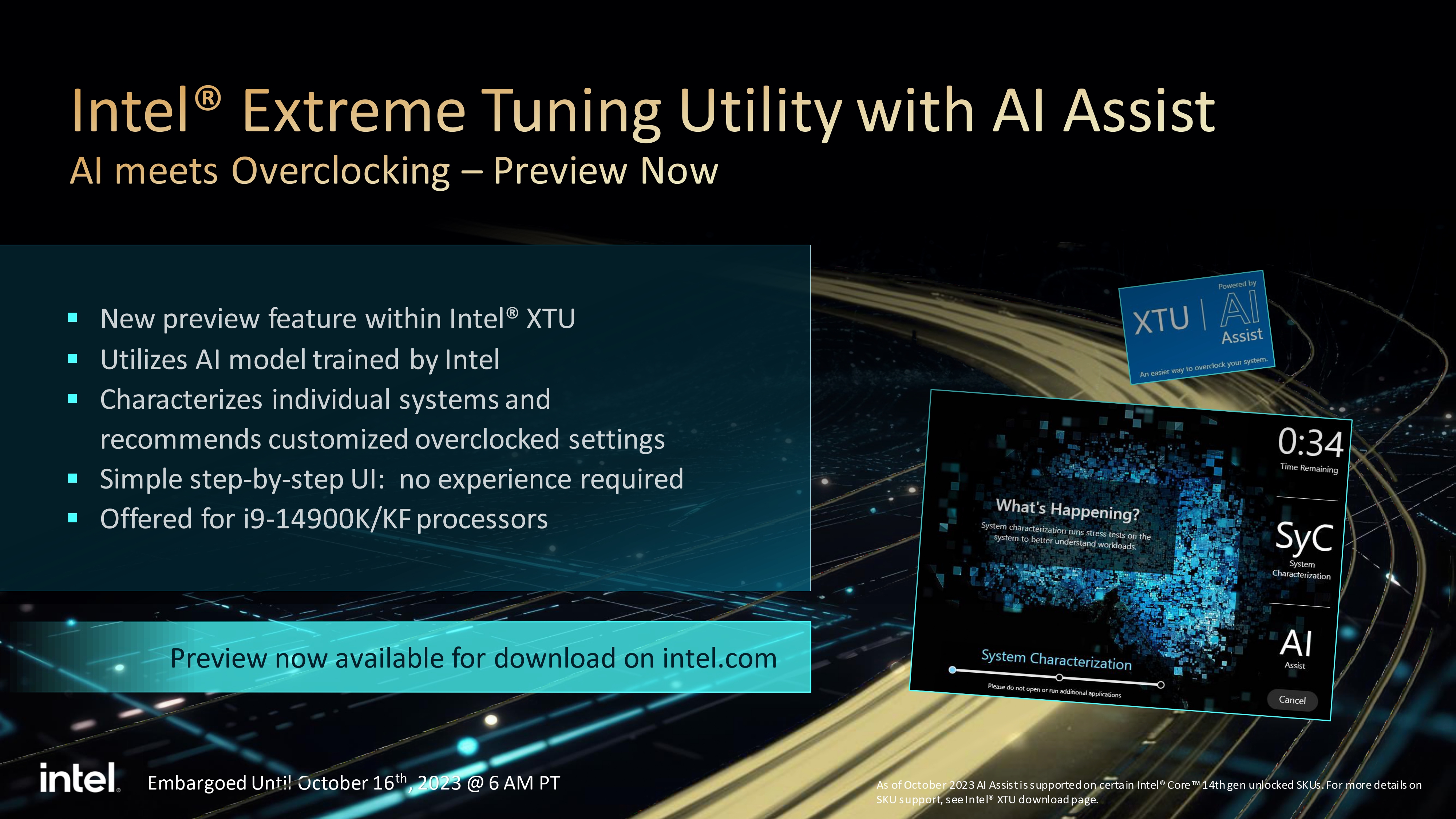
Of course, it should be noted that overclocking does, in fact, void Intel's warranty, so users should use this feature at their own risk.
Intel boasts up to 23% better gaming performance with their in-house testing than Intel's 12th Gen Core series (Alder Lake), the first platform to bring the hybrid core architecture to Intel's desktop lineup. It must be noted that Intel hasn't compared performance directly to 13th Gen (Raptor Lake), likely due to the close similarities both families share: same cores, same architecture, just slightly faster frequencies out of the box.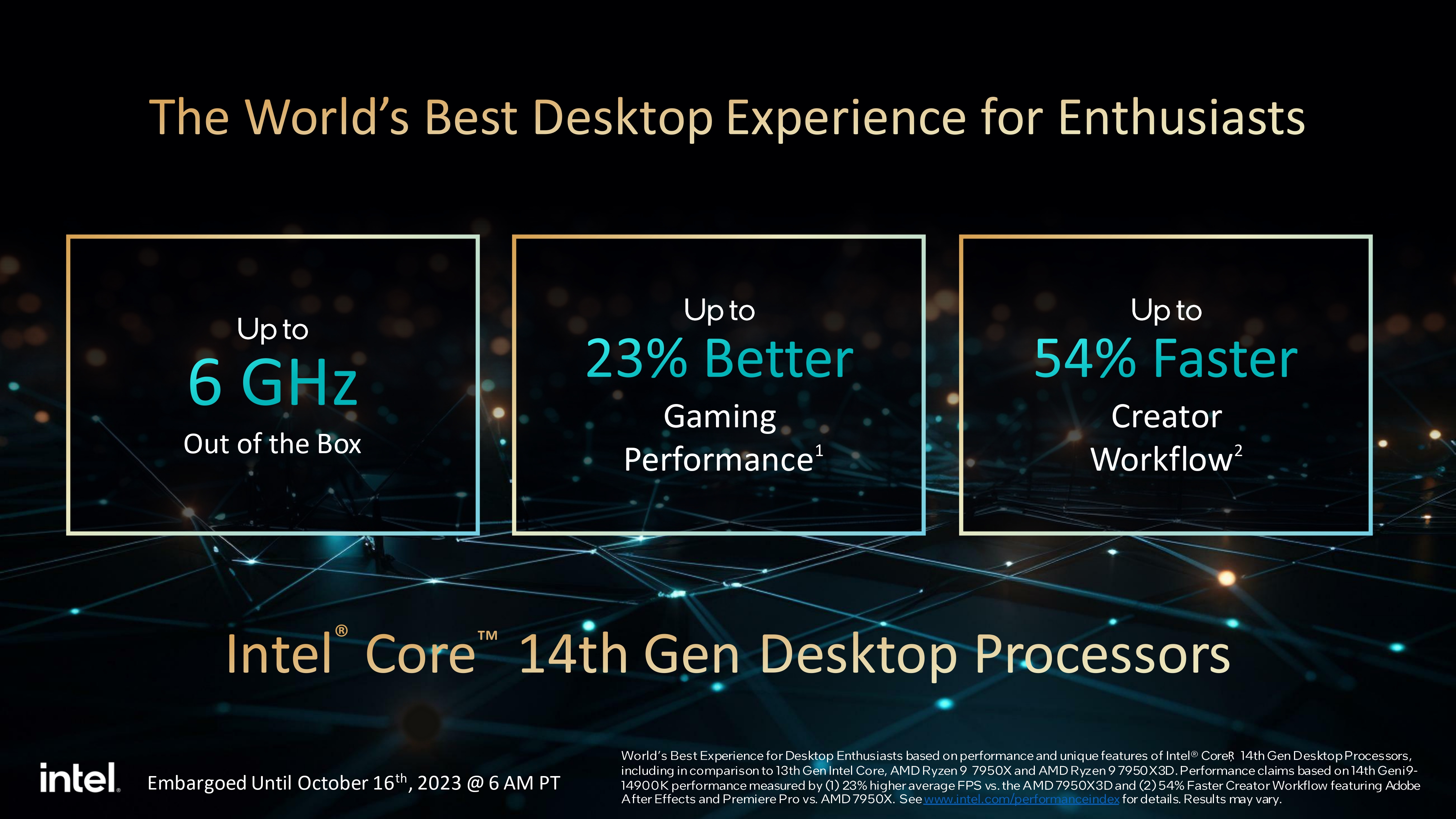
The Intel 14th Gen chips are designed for the preexisting 600 and 700-series motherboards, which use the LGA 1700 socket. Motherboard vendors have already begun refreshing their Z790 offerings with more modern features, such as Wi-Fi 7 and Bluetooth 5.4, providing motherboard manufacturers decide to integrate them into their refreshed Z790 models. Official memory compatibility remains the same as 13th Gen, supporting DDR5-5600 and DDR4-3200 memory. Though overclockers may find the highest binned chips more capable than before, with Intel teasing speeds beyond DDR5-8000 for their best chips.
The Intel 14th Gen Core family of desktop processors (K and KF) is launching on October 17th at retailers and system integrators. Pricing-wise, the flagship Core i9-14900K costs $589, the Core i7-14700K will be available for $409, and the more affordable Core i5-14600K for $319.
Gallery: Intel Announces 14th Gen Core Series For Desktop:_page-0001_thumb.jpg)
_page-0002_thumb.jpg)
_page-0003_thumb.jpg)
_page-0004_thumb.jpg)
_page-0005_thumb.jpg)
_page-0006_thumb.jpg)
More...
-
10-16-23, 11:02 PM #11913
Anandtech: TSMC: We Want OSATs to Expand Their Advanced Packaging Capability
Almost since the inception of the foundry business model in the late 1980s, TSMC would produce silicon. In contrast, an outsourced semiconductor assembly and test (OSAT) service provider would then package it into a ceramic or organic encasing. Things have changed in recent years with the emergence of advanced packaging methods that require sophisticated tools and cleanrooms that are akin to those used for silicon production because TSMC was at the forefront of innovative packaging methods, which the company aggregates under the 3DFabric brand and because it built appropriate capacity, it quickly emerged as a significant OSAT for advanced packaging.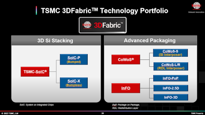
Many companies, such as Nvidia, want to send in blueprints and get their product that is ready to ship, which is why they choose to use TSMC's services to package their advanced system-in-packages, such as H100, using such technologies as integrated fan-out (InFO, chip first) and chip-on-wafer-on-substrate (CoWoS, chip last) developed by the foundry. As a result, TSMC had to admit earlier this year that it could not keep up with CoWoS demand and would expand appropriate production capacity.
Although TSMC makes tons of money on advanced chip packaging methods these days, the company does not have plans to steal business away from its traditional OSAT partners, which is why it wants these companies to expand their sophisticated packaging capacity and use similar tools to TSMC and its partners to offer to package compatible with TSMC-made chiplets.
But it is not that simple. All leading assembly and test specialists like ASE Group, Amkor Technology, and JCET have advanced chip packaging technologies, many resembling those of TSMC. These OSATs own advanced packaging fabs already and can serve fabless chip designers. For example, just this week, Amkor opened up its $1.6 billion advanced packaging facility in Vietnam. It is set to have a cleanroom space comparable to that GlobalFoundries owns across multiple fabs.
But while packaging technologies offered by OSATs may be similar to those of TSMC in terms of pitch dimensions and bump I/O pitch dimensions, they are not the same in terms of flow and may even have slightly different electric specifications. Meanwhile, OSATs use the same tools as TSMC, so they can pack chips that use CoWoS interposer. So far, TSMC has certified two OSATs to perform the final CoWoS assembly. However, there is still a shortage of CoWoS capacity on the market because TSMC's capacity is the bottleneck, at least based on TSMC's comments from earlier this year.
"So, we have ASE and SPIL, we have qualified their substrates," said Dan Kochpatcharin, Head of Design Infrastructure Management at TSMC, at the OIP 2023 conference in Amsterdam. "The next step is also doing the same thing to bring them into using the automated routing of the substrate as well. So, we can have the whole [CoWoS service] stack."
TSMC's advanced packaging technologies like CoWoS and InFO are supported by electronic design automation (EDA) tools from companies like Ansys, Cadence, Siemens EDA, and Synopsys. So, TSMC needs OSATs to use the same programs and align their technical capabilities with what these tools design and TSMC produces.
"We want them to use the same EDA tools," said Kochpatcharin. "So, let's say TSMC interposer on OSAT's substrate. So, they use 3Dblox and [appropriate] EDA tools to do analysis, then it is easier for the customer. Right? Like we qualified the two partners to [produce] substrate. So, we do CoWoS, and OSATs do substrate. So, it would be good to use the same flow, because it is easier for customer. "If you have customers who use [different EDA tools] then the multi physics analysis [of the package] will be more difficult. It can be done just more difficult."
To meet the demand for CoWoS and other advanced packaging methods, OSATs need to invest in appropriate capacities and tools, which are expensive. The problem is that assembly and test specialists cannot keep up with Intel, TSMC, and Samsung regarding investments in advanced packaging facilities. Last year, Intel spent $4 billion on advanced packaging plants, and TSMC's capital expenditures on advanced packaging totaled $3.6 billion. In contrast, Samsung spent around $2 billion, according to Yole Group's estimates published by EE Times. By comparison, the capital expenditures of ASE Group (with SPIL and USI) totaled $1.7 billion in 2022, whereas the spending of Amkor reached $908 million.
There are several reasons why advanced packaging technologies like TSMC's CoWoS and InFO, as well as Intel's EMIB and Foveros, are gaining importance. First up, disaggregated chip designs are getting more popular because chip manufacturing is getting more expensive, smaller chips are easier to yield, and many chips are reaching the reticle limit. At the same time, their designers want them to be bigger and more powerful. Secondly, disaggregated designs using chiplets made on different nodes are cheaper than one monolithic chip on a leading-edge node.
OSATs are poised to expand their advanced production capacities as their clients demand appropriate services. Meanwhile, they are less inclined to offer such services than foundries simply because if something fails during packaging steps, they have to throw away all the expensive silicon they package, and they do not earn as much as chipmakers do. Their margins are also significantly lower. Finally, it may be unclear in many cases why a multi-chiplet package does not work and whether the problem is with the package itself or with one of the chips. Today, all TSMC can do is to optically check the wafers before dicing them, but this is not a particularly efficient way of testing.
To gain the capability to test chiplets individually, TSMC is working with makers of chip test equipment and expects to validate these tools next year.
"On the 3DFabric on the testing, we work with Advantest, Teradyne, and Synopsys to leverage the high-speed die-to-die testing," said Kochpatcharin. "When you have all these things stacked together, it is getting very difficult to test them. So, we have worked with Teradyne and Advantest to work […] [die-to-die] testing, and we will have silicon validation in 2024."
More...
-
10-17-23, 12:46 PM #11914
Anandtech: Canon Prepares Nanoimprint Lithography Tool To Challenge EUV Scanners
Canon has recently revealed its FPA-1200NZ2C, a nanoimprint semiconductor manufacturing tool that can be used to make advanced chips. The device uses nanoimprint lithography (NIL) technology as an alternative to photolithography, and can theoretically challenge extreme ultraviolet (EUV) and deep ultraviolet (DUV) lithography tools when it comes to resolution.
Unlike traditional DUV and EUV photolithography equipment that transfers a circuit pattern onto a resist-coated wafer through projection, nanoimprint tool employs a different technique. It uses a mask, embossed with the circuit pattern, which directly presses against the resist on the wafer. This method eliminates the need for an optical mechanism in the pattern transfer process, which promises a more accurate reproduction of intricate circuit patterns from the mask to the wafer. In theory, NIL enables formation of complex two- or three-dimensional circuit patterns in a single step, which promises to lower costs. NIL itself is not a new technology, but it has remained in parallel development over the years, while the challenges involved in further improving photolithography have Canon believing that now is a good time for a second-look.
Canon says that its FPA-1200NZ2C enables patterning with a minimum linewidth (critical dimensions, CD) of 14 nm, which is good enough to 'stamp' a circa 26-nm minimum metal pitch, and therefore suitable for 5 nm-class process technologies. That would be in line with capabilities of ASML's Twinscan NXE:3400C (and similar) EUV lithography scanners with a 0.33 numerical aperture (NA) optics.
Meanwhile, Canon says that further refinements of its technology, its tool can achieve finer resolutions that can enable 3 nm and even 2 nm-class production nodes.
Nanoimprint lithography offers several compelling advantages over photolithography. Primarily, NIL excels in resolution, enabling the creation of structures at the nanometer scale with remarkable precision without using photomasks. This technology bypasses the diffraction limits encountered in conventional photolithography, allowing for more intricate and smaller features. Additionally, NIL operates without the necessity of complex optics or high-energy radiation sources, leading to potentially lower operational costs and simpler equipment.
Another advantage of NIL is its direct patterning capability, enabling the reproduction of three-dimensional nanostructures effectively. Such functionality makes NIL a potent tool in the production of photonics and other applications where three-dimensional nano-patterns are essential. The technology also facilitates better pattern fidelity and uniformity.
However, NIL also presents certain challenges and limitations. One notable issue is its susceptibility to defects due to the direct contact involved in the imprinting process. Particles or contaminants present on the substrate or the mold can lead to defects, which may affect the overall yield and reliability of the manufacturing process. This necessitates impeccable process control and cleanliness to maintain consistent output quality.
Additionally, NIL, in its traditional form, is a serial process, which limits its throughput and production capacity. Unlike photolithography, which can process entire wafers or large areas in a parallel fashion, NIL often involves processing smaller areas sequentially. This poses great challenges in scaling the technology for high-volume manufacturing of chips, which limits its usage for chip manufacturing. Meanwhile, NIL can be used to create photomasks for EUV and DUV. Also, it can theoretically be used to create patterned media for hard disk drives.
More...
-
10-17-23, 12:46 PM #11915
Anandtech: Intel Core i9-14900K, Core i7-14700K and Core i5-14600K Review: Raptor Lak
In what is to be the last of Intel's processor families to use the well-established Core i9, i7, i5, and i3 naming scheme, Intel has released its 14th Generation Core series of desktop processors, aptly codenamed Raptor Lake Refresh (RPL-R). Building upon the already laid foundations of the 13th Gen Core series family, Intel has announced a variety of overclockable K and KF (no iGPU) SKUs, including the flagship Core i9-14900K, the reconfigured Core i7-14700K, and the cheaper, yet capable Core i5-14600K.
The new flagship model for Intel's client desktop products is the Core i9-14900K, which looks to build upon the Core i9-13900K, although it's more comparable to the special edition Core i9-13900KS. Not only are the Core i9-14900K and Core i9-13900KS similar in specifications, but the Core i9-14900K/KF are the second and third chips consecutively to hit 6.0 GHz core frequencies out of the box.
Perhaps the most interesting chip within Intel's new 14th Gen Core series family is the Core i7-14700K, which is the only chip to receive an uplift in cores over the previous SKU, the Core i7-13700K. Intel has added four more E-cores, giving the Core i7-13700K a total of 8 P-cores and 12 E-cores (28 threads), with up to a 5.6 GHz P-core turbo and a 125 W base TDP; the same TDP across all of Intel's K and KF series 14th Gen core chips.
Also being released and reviewed today is the Intel Core i5-14600K, which has a more modest 6P+8E/20T configuration and has the same configuration 5.3 GHz boost frequency and 3.5 GHz base frequency on the P-cores as the Core i5-13600K. Intel has only boosted the E-core boost frequency by 100 MHz to justify the Core i5-14600K, which means it should perform similarly to its predecessor.
Despite being a refreshed selection of Intel's 13th Gen Raptor Lake platform, the biggest question, aside from the performance, is what are the differences, and are there any nuances to speak of, and how do they correlate regarding performance to 13th Gen? We aim to answer these questions and more in our review of the Intel 14th Gen Core i9-14900K, Core i7-14700K and Core i5-14600K processors.
More...
-
10-18-23, 09:30 PM #11916
Anandtech: Arm Total Design to Facilitate Development of Custom Datacenter SoCs
Arm this week introduced its Arm Total Design initiative, which is aimed at accelerating development of custom datacenter-oriented system-on-chip (SoC) designs using Neoverse Compute Subsystems (CSS). The collaborative ecosystem unites various developers in a bid to speed up time-to-market and reduce development costs of custom SoCs for AI, cloud, and high-performance computing markets. ATD promises to enable development of datacenter processors that will offer formidable competition for x86 CPUs.
The Arm Total Design ecosystem is a conglomerate of ASIC design houses, IP vendors, EDA tool providers, foundries, and firmware developers that is aimed to facilitate rapid and cost-efficient delivery of custom silicon for datacenters based on Arm Neoverse cores for AI, HPC, cloud, and networking workloads. The ecosystem provides preferential access to Neoverse CSS to its partners, fostering innovation, and facilitating faster time-to-market strategies, while also lowering development costs.
The initiative aims to harness collective industry expertise at every stage of custom SoC development, thereby promoting the broad availability of specialized, Arm Neoverse-based solutions.

Central to this initiative is the delivery of pre-integrated, validated IP and EDA tools, courtesy of collaborative efforts from partners such as Cadence, Rambus, and Synopsys. Such strategic collaborations are instrumental in speeding up silicon design process as it simplifies incorporation of essential components like memory, security, and various peripherals.
In addition to the abovementioned companies, Arm Total Design leverages design services prowess of such companies ADTechnology, Alphawave Semi, Broadcom, Capgemini, Faraday, Socionext, and Sondrel. These companies bring their expertise to the table, providing robust support to the ecosystem given their experience with Neoverse CSS as well as other Arm IPs and technologies.
Since the expected future of datacenter processors is multi-chiplet, the Arm Total Design ecosystem not only makes custom chips more accessible, but also poised to support AMBA CHI C2C, and UCIe standards. Intel Foundry Services and TSMC also participate in the Arm Total Design ecosystem bringing in leading-edge process technologies and advanced packaging techniques.
Complementing the hardware-focused aspects, the initiative also places a strong emphasis on commercial software and firmware support for Neoverse CSS, drawing upon the specialized contributions from AMI.
On paper, Arm Total Design emerges as a major alliance that could significantly alter the landscape of custom datacenter silicon development. By combining a diverse spectrum of industry leaders under one roof, it promises a seamless and efficient pathway towards realizing the potentials of Neoverse CSS. This collaborative venture aspires to unlock new levels of performance and features for AI, edge, and HPC SoCs based on the Arm technology, offering a decidedly more group-oriented approach to chip design than the vertically integrated strategies employed by industy heavyweights such as Intel and AMD.
More...
-
10-18-23, 09:30 PM #11917
Anandtech: Qualcomm Swaps Out Arm for RISC-V for Next-Gen Google Wear OS Devices
As part of a broad collaborative agreement with Google, Qualcomm this week said that that it will be adopting the RISC-V instruction set architecture (ISA) for a future Snapdragon Wear platform. Working together, the two companies will be bootstrapping a RISC-V ecosystem for Wear OS devices, with Qualcomm providing the hardware while Google expands its wearables OS and associated ecosystem of tools to support the new processor architecture.
Qualcomm's Wear processors have been the de facto chip of choice for Wear OS devices since the launch of Google's wearables platform almost a decade ago, with Qualcomm employing multiple generations of Arm CPU designs. This makes Qualcomm's decision to develop a RISC-V wearables SoC especially significant, as it not only represents one of the highest profile adoptions of RISC-V in a consumer platform to date, but it means that, depending on Qualcomm's specific product plans, this could see the overall Wear OS market make a hard turn from Arm to RISC-V in relatively short order.
As laid out in the relatively brief announcement from Qualcomm, the company will focus on development of RISC-V-based hardware suitable for wearable devices. While the company isn't disclosing detailed technical specifications of their in-development products, given the company's significant chip-design background, this likely includes customized RISC-V general purpose cores as well as sensors.
Notably here, the announcement is for "a RISC-V based wearables solution," rather than a complete pivot to RISC-V with multiple solutions. Wearables as a whole are a much smaller market than smartphones, so Qualcomm has historically not offered a particularly deep lineup of hardware – meaning that even one chip is significant. Still, this also means that Qualcomm is not formally dropping Arm from its Snapdragon Wear platform at this time.
Qualcomm's decision to embrace RISC-V for a future wearables SoC is significant news for the up-and-coming ISA, as this marks one of the highest profile adoptions of RISC-V in consumer gear to date. The open standard ISA has seen success over the last several years in the microcontroller market, with chip vendors adopting RISC-V CPU cores – often in place of Arm Cortex-M designs – as a means of having more control over their CPU core designs, and avoid paying ISA royalties in the process. Conversely, RISC-V has seen very limited adoption in the application processor space thus far, owing to the more complex chip designs and the overall smaller market. So Qualcomm's plans to use RISC-V in their Snapdragon Wear platform, which has traditionally been based on Arm Cortex-A designs, marks a significant milestone for the adoption of RISC-V into higher-performing mobile devices.
Similarly, Google's backing of the ISA by porting Wear OS to RISC-V is a major milestone on the software front. Bootstrapping a platform based on a new ISA is not just about the hardware, but the software as well, as there needs to be well-developed operating systems and applications to make the hardware useful. All of which requires significant tooling to enable that development. Google, for its part, is no stranger to embracing multiple ISAs – Android has long supported Arm, x86, and even MIPS – and the company already announced earlier this year that they're working to make RISC-V a "tier-1" platform for Android, so the company's efforts with Wear OS will go hand-in-hand with that.
Between the two companies, Google and Qualcomm essentially make up the software and hardware backend of the Wear OS ecosystem. Google's Wear OS, in turn, is used by a range of popular smart watches, including those from Samsung, Fossil Group, Motorola, and Casio.
"Qualcomm Technologies have been a pillar of the Wear OS ecosystem, providing high performance, low power systems for many of our OEM partners," said Bjorn Kilburn, GM of Wear OS by Google. "We are excited to extend our work with Qualcomm Technologies and bring a RISC-V wearable solution to market."
Meanwhile, the decision to use RISC-V for wearables also has the potential to be a big change for the business side of Qualcomm. The company is current butting heads with Arm over licensing and royalty rates, particularly in regards to their acquired Nuvia IP. That relationship has already devolved to lawsuits, including Arm looking to block Qualcomm's use of Nuvia-designed Arm CPU cores.
In short, swapping out Arm for RISC-V would allow Qualcomm to do away with paying royalties to Arm for Snapdragon Wear chips. The current royalties aren't thought to be extravagant – Qualcomm is using Cortex-A53 here – but a penny saved is a penny booked for Qualcomm's quarterly earnings. If nothing else, the very public announcement about the development of a RISC-V Snapdragon Wear SoC can be considered a shot across Arm's bow, as a reminder that Qualcomm could eventually do the same thing with bigger and higher royalty bearing chips.
"We are excited to leverage RISC-V and expand our Snapdragon Wear platform as a leading silicon provider for Wear OS," said Dino Bekis, vice president and general manager, Wearables and Mixed Signal Solutions, Qualcomm Technologies. " Our Snapdragon Wear platform innovations will help the Wear OS ecosystem rapidly evolve and streamline new device launches globally."
More...
-
10-19-23, 05:39 PM #11918
Anandtech: TSMC Q3 Earnings: 3nm Production Node Accounts for 6% of Revenue
Although Taiwan Semiconductor Manufacturing Co. formally started production of chips using its N3 (3nm-class) process technology back in late 2022, the company did not recognize any meaningful N3 revenue in Q1 and Q2. This week as part of the company's Q3 earnings announcement, the foundry finally recognized its first N3-related revenue, with N3 accounting for 6% of TSMC's Q3 revenue. Meanwhile, advanced nodes now account for 59% of TSMC's earnings.
For their first quarter of significant 3nm revenue, TSMC booked roughly $1.03 billion in income for the new node. To put the number into generational context, TSMC recognized its first N5 revenue in Q3 2020, where back then the technology accounted for $0.97 billion in revenue making 5nm-class chips – or about 8% of TSMC's revenue share.
The strong start to N3 revenue was not unexpected, if only due to the ever-rising prices that TSMC is thought to charge for their cutting-edge wafers. Still, even with a billion dollar quarter, TSMC is just getting started; the company previously warned that its 3nm ramp would take some time.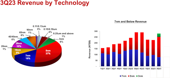
Going forward, TSMC's long-term plans for the 3nm node call for the company to eventually offer several variations on the process. TSMC's baseline N3 (aka N3B) node uses up to 25 EUV layers, some with expensive EUV double-patterning, allowing higher transistor density but at higher costs – and few customers. More clients have opted for the more cost-efficient N3E process technology with up to 19 EUV layers, no EUV double-patterning, offering lower logic density, but better yields and a wider process window. TSMC is set to begin to ramp up N3E in Q4 2024 and with this version its 3nm-class process technology is expected to shine.
"Our business in the third quarter was supported by the strong ramp of our industry-leading 3nm technology and higher demand for 5nm technologies, partially offset by customers' ongoing inventory adjustment," said C.C. Wei, chief executive of TSMC, at the conference call with analysts and investors. "N3 is already involving production with good yield, and we are seeing a strong ramp in the second half of this year, supported by both HPC and smartphone applications. […] N3E has passed qualification and achieved performance and yield targets and will start volume production in fourth quarter of this year. "
TSMC's total revenue Q3 2023 hit $17.28 billion, a 14.6% decrease year-over-year, but a 10.2% increase from the previous quarter. Meanwhile, the company's net income increased 16.1% quarter-over-quarter to $6.521 billion, whereas gross margin for the quarter was 54.3%
More...
-
10-19-23, 05:39 PM #11919
Anandtech: Seagate Unveils Exos X24 24TB and 28 TB: Setting the Stage for HAMR HDDs
Seagate on Wednesday introduced its Exos X24 family of hard drives, it's highest capacity series of drives to date. The new family is comprised of both conventional magnetic recording technology (CMR) and shingled magnetic recording (SMR) models, with the CMR drive topping out at 24 TB, while SMR brings the peak capacity up to 28 TB. Both are, as of now, the highest-capacity HDDs in their respective segments. But perhaps the most important technological development with the Exos X24 lineup is that it uses a platform that will be largely re-used for the upcoming HAMR drives.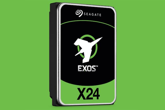
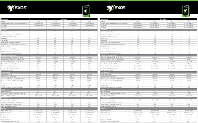
The Seagate Exos X24 3.5-inch helium-filled hard drive family includes 12 TB, 16 TB, 20 TB, and 24 TB models, which are built using up to 10 2.4 TB platters. Seagate's platters feature perpendicular magnetic recording (PMR) and heads utilizing two-dimensional magnetic recording (TDMR) technology (to minimize adjacent track interference and ensure reliable reading at high track pitch densities). In addition, Seagate offers a sole 28 TB SMR version of the Exos X24 to select cloud customers who can self-manage shingled recording in their datacenters.
Seagate's Exos X24 HDDs operate at a spindle speed of 7200 RPM and feature a segmented 256 MB cache (check out all of its specifications in tables below). The family's 2.4 TB platters have an areal density of 1260 Gbit/inch2, allowing for a peak sustained transfer rate of 285 MB/s, which is in line with previous-generation HDDs (which is a bit surprising as typically higher areal density enables higher transfer rates). The entire Exos X24 range offers up to 168/550 random read/write IOPS (4K, QD16), which is again in line with previous-generation drives.
Seagate plans to make the Exos X24 HDDs available with either a SATA 6 Gbps or a dual-port SAS 12 Gbps interface to cater to varying customer needs.
As for power consumption of Exos X24, it ranges from 6.3W (idle) to 8.9W (max) for SATA versions and from 6.5W (idle) to 9.8W (max) for the SAS SKUs. Exos X24 HDDs are also adaptable to meet the diverse needs of major clients, supporting PowerBalance technology, which offers data centers the ability to harmonize power usage with IOPS performance. Additionally, they feature PowerChoice technology, optimizing power consumption during periods of inactivity.
The enterprise-focused drives otherwise check all of the usual boxes for this market segment, including vibration resistance and RV sensors. The drives are rated to handle workloads up to 550 TB/year, with a 5 year overarching warranty.Seagate Exos X24 - Metrics of Interest Rated Workload (TB/yr) 550 Max. Sustained Transfer Rate (MBps) 285 Random Read/Write 4K QD16 WCD (IOPS) 168/550 Areal Density 1260 Gbit/inch2 Rated Load / Unload Cycles 600K Unrecoverable Read Errors 1 in 10E15 MTBF (Hours) 2.5M Power (Idle / Active) (W) SATA: 6.3W - 8.9W | SAS: 6.5W - 9.8W Warranty (Years) 5 Datasheet PDF
Seagate said it had commenced shipping of qualification Exos X24 drives to select customers, and the production drives are slated to be widely available for channel distribution in December.
Finally, and most interesting of all, the company has also revealed that the 10-platter helium-sealed platform will be significantly re-used for the company's upcoming heat-assisted magnetic recording (HAMR) hard drives. Those drives will be available in capacities up to 32 TB, with Seagate set to ramp up production in early 2024.
More...
-
10-20-23, 05:28 PM #11920
Anandtech: Samsung Announces 'Shinebolt' HBM3E Memory: HBM Hits 36GB Stacks at 9.8 Gb
Samsung’s annual Memory Tech Day is taking place in San Jose this morning, and as part of the event, the company is making a couple of notable memory technology announcements/disclosures. The highlight of Samsung’s event is the introduction of Shinebolt, Samsung’s HBM3E memory that will set new marks for both memory bandwidth and memory capacity for high-end processors. The company is also disclosing a bit more on their GDDR7 memory, which will mark a significant technological update to the GDDR family of memory standards.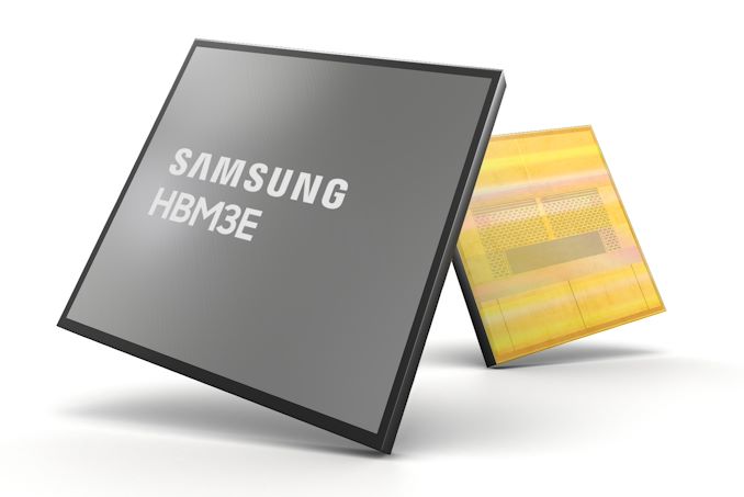
More...


 Quote
QuoteThread Information
Users Browsing this Thread
There are currently 15 users browsing this thread. (0 members and 15 guests)


Bookmarks