

Results 12,001 to 12,010 of 12089
Thread: Anandtech News
-
01-17-24, 10:00 PM #12001
Anandtech: AMD Rolls Out Radeon RX 7900 XT Promo Pricing Opposite GeForce RTX 40 Supe
In response to the launch of NVIDIA's new GeForce RTX 40 Super video cards, AMD has announced that they are instituting new promotional pricing on a handful of their high-end video cards in order to keep pace with NVIDIA's new pricing.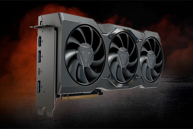
Kicking off what AMD is terming a special "promotional pricing" program for the quarter, AMD has been working with its retail partners to bring down the price of the Radeon RX 7900 XT to $749 (or lower), roughly $50 below its street price at the start of the month. Better still, AMD's board partners have already reduced prices further than AMD's official program/projections, and we're seeing RX 7900 XTs drop to as low as $710 in the U.S., making for a $90 drop from where prices stood a few weeks ago.
Meanwhile, AMD is also technically bringing down prices on the China and OEM-only Radeon RX 7900 GRE as well. Though as this isn't available for stand-alone purchase on North American shelves, it's mostly only of relevance for OEM pre-builds (and the mark-ups they charge).
Ultimately, the fact that this is "promotional pricing" should be underscored. The new pricing on the RX 7900 XT is not, at least for the moment, a permanent price cut. Meaning that AMD is leaving themselves some formal room to raise prices later on, if they choose to. Though in practice, it would be surprising to see card prices rebound – at least so long as we don't get a new crypto boom or the like.
Finally, to sweeten the pot, AMD is also extending their latest game bundle offer for another few weeks. The company is offering a copy of Avatar: Frontiers of Pandora with all Radeon RX 7000 video cards (and select Ryzen 7000 CPUs) through January 30, 2024.
More...
-
01-18-24, 10:49 AM #12002
Anandtech: Apple to Cut Blood Oxygen Feature from Newly-Sold Apple Watches in the U.S
Following the latest legal defeat in Apple's ongoing patent infringement fight over blood oxygen sensors, the company is set to remove its blood oxygen measurement feature from its Watch Series 9 and Watch Ultra 2 sold in the U.S. The decision comes after the U.S. Court of Appeals for the Federal Circuit declined to extend a pause on an import ban imposed by the U.S. International Trade Commission (USITC) last year, making way for the ban to finally take effect.
The legal setback stems from a ruling that Apple's watches infringed on patents related to blood oxygen measurement that belong to Masimo, which sued Apple in 2020. The U.S. Court of Appeals' decision means that Apple must stop selling watches with this feature while the appeal, which could last a year or more, is in progress.
As the ruling bars Apple from selling additional watches with this feature, the company has been left with a handful of options to comply with the ruling. Ceasing watch sales entirely certainly works – though is unpalatable for obvious reasons – which leaves Apple with removing the feature from their watches in some manner. Any hardware retool to avoid infringing upon Masimo's patents would take upwards of several quarters, so for the immediate future, Apple will be taking the unusual step of disabling the blood oxygen sensor feature in software instead, leaving the physical hardware on-device but unused.
The new, altered Apple Watch models will be available from Thursday in Apple's retail and online stores. Despite the change, the company maintains that the USITC's decision is erroneous and continues to appeal. Apple stresses that the blood oxygen feature will still be available in models sold outside the U.S., and perhaps most critically, watches sold in the U.S. before this change will keep their blood oxygen measuring capability.
"Pending the appeal, Apple is taking steps to comply with the ruling while ensuring customers have access to Apple Watch with limited disruption," the company said in a statement published by Bloomberg.
It is noteworthy that the Patent Trial and Appeal Board invalidated 15 of 17 Masimo's patents it reviewed, a verdict that Masimo is currently challenging. In Masimo's trial for trade secret misappropriation last May, a judge ruled out half of Masimo's 10 allegations due to a lack of adequate evidence. Regarding the remaining allegations, most jurors agreed with Apple's position, but the trial ultimately ended with an 11-1, non-unanimous decision, resulting in a mistrial. Scheduling of a new trial to settle the matter is still pending. In the meantime, Apple has been left with little choice but to downgrade its products to keep selling them in the U.S.
More...
-
01-19-24, 08:51 PM #12003
Anandtech: TSMC 2nm Update: Two Fabs in Construction, One Awaiting Government Approva
When Taiwan Semiconductor Manufacturing Co. (TSMC) is prepping to roll out an all-new process technology, it usually builds a new fab to meet demand of its alpha customers and then either adds capacity by upgrading existing fabs or building another facility. With N2 (2nm-class), the company seems to be taking a slightly different approach as it is already constructing two N2-capable fabs and is awaiting for a government approval for the third one.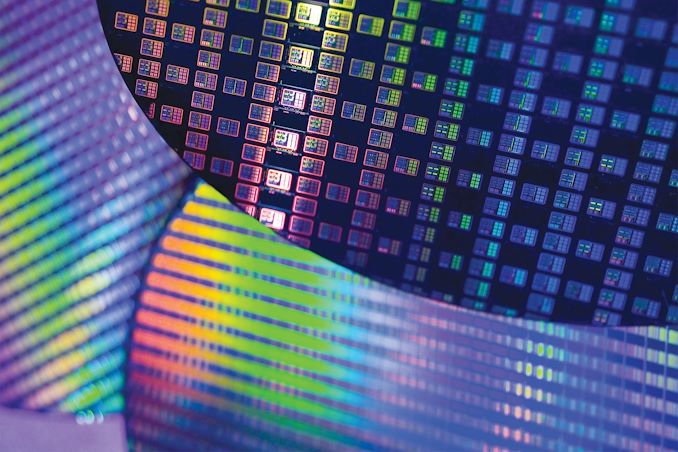
We are also preparing our N2 volume production starting in 2025," said Mark Liu, TSMC's outgoing chairman, at the company's earnings call with financial analysts and investors. "We plan to build multiple fabs or multiple phases of 2nm technologies in both Hsinchu and Kaohsiung science parks to support the strong structural demand from our customers. […] "In the Taichung Science Park, the government approval process is ongoing and is also on track."
TSMC is gearing up to construct two fabrication plants capable of producing N2 chips in Taiwan. The first fab is planned to be located near Baoshan in Hsinchu County, neighboring its R1 research and development center, which was specifically build to develop N2 technology and its successor. This facility is expected to commence high-volume manufacturing (HVM) of 2nm chips in the latter half of 2025. The second N2-capable fabrication plant by is to be located in the Kaohsiung Science Park, part of the Southern Taiwan Science Park near Kaohsiung. The initiation of HVM at this plant is projected to be slightly later, likely around 2026.
In addition, the foundry is working to get government approvals to build a yet another N2-capable fab in the Taichung Science Park. If the company starts to construct this facility in 2025, the fab could go online as soon as in 2027.
With three fabs capable of making chis using its 2nm process technologies, TSMC is poised to offer vast 2nm capacity for years to come.
TSMC expects to start HVM using its N2 process technology that uses gate-all-around (GAA) nanosheet transistors around the second half of 2025. TSMC's 2nd generation 2nm-class process technology — N2P — will add backside power delivery. This technology will be used for mass production in 2026.
More...
-
01-19-24, 08:51 PM #12004
Anandtech: TSMC Posts Q4'23 Earnings: 3nm Revenue Share Jumps to 15%, 5nm Overtakes 7
Taiwan Semiconductor Manufacturing Co. released its Q4'2023 and full year 2023 financial results this week. And along with a look at the financial state of the firm as it enters 2024, the company's earnings info also offers a fresh look at the utilization of their various fab nodes. Of particular interest, with TSMC ramping up production of chips on its N3 (3 nm-class) process technology, N3 (aka N3B) has already reached the point where it accounts for 15% of TSMC's revenue in Q4 2023. This is a very fast – albeit not record fast – revenue ramp.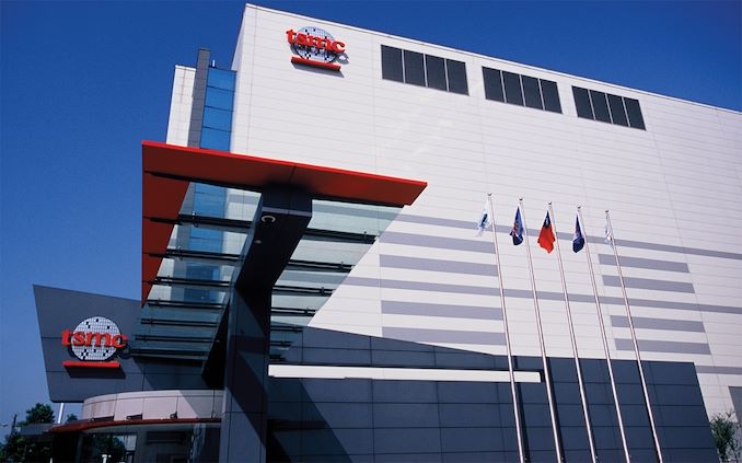
In the fourth quarter of 2023, sales of wafers processed using N3 accounted for 15% of TSMC's total wafer revenue, whereas revenue of N5 and N7 accounted for 39% and 17% respectively. In terms of dollars, N3 revenue for TSMC was $2.943 billion, N5 sales totaled $6.867 billion, and N7 revenue reached $3.3354 billion. In general, advanced technologies (N7, N5, N3) commanded 67% of TSMC's revenue, whereas the larger grouping of FinFET-based process technologies accounted for 75% of the company's total wafer revenue.
It is noteworthy that revenue share contributions made by system-on-chips (SoCs) for smartphones and high-performance computing (a vague term that TSMC uses to describe everything from game consoles to notebooks and from workstations to datacenter-grade processors) were equal in Q4 2023: 43% each. Automotive chips accounted for 5%, and Internet-of-Things chips contributed another 5%.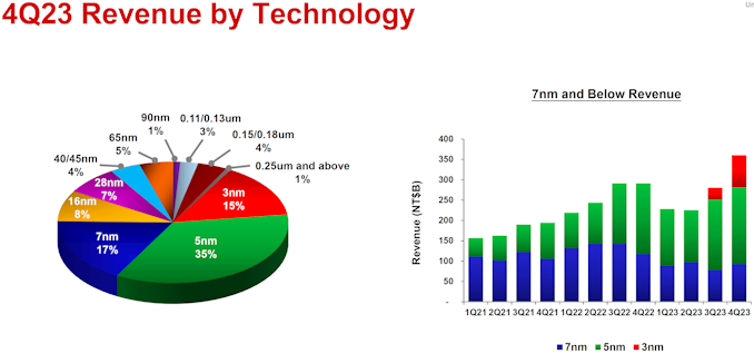
"Our fourth quarter business was supported by the continued strong ramp of our industry-leading 3-nanometer technology," said Wendell Huang, VP and Chief Financial Officer of TSMC. "Moving into first quarter 2024, we expect our business to be impacted by smartphone seasonality, partially offset by continued HPC-related demand."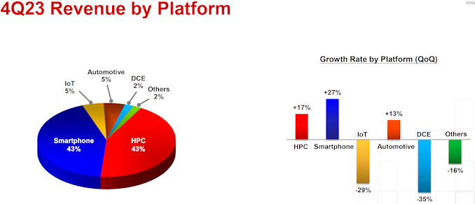
To put TSMC's N3 revenue share ramp into context, we need to compare it to the ramp of the foundry's previous-generation all-new node: N5 (5 nm-class), which entered high-volume manufacturing in mid-2020. TSMC began to recognize its N5 revenue in Q3 2020 and the production node accounted for 8% of the company's sales back then, which totaled $0.97 billion. In the second quarter of its availability (Q4 2020), N5 accounted for 20% of TSMC's revenue, or $2.536 billion.
There is a major catch about TSMC's N5 ramp in 2020 that muddles comparisons a bit, however. The world's largest contract maker of chips sold boatload of N5-based system-on-chips to Huawei at the time (shipping them physically before the U.S. sanctions against the company became effective in September, 2020) as well as Apple. By contrast, it is widely believed that Apple is the sole client to use TSMC's N3B technology due to costs. Which means that, even with the quick ramp, TSMC has fewer customers in the early days of N3 than they did in N5, contributing to the slower ramp for N3.
As for the entire year, N3 wafer revenue account for 6% of TSMC's total wafer revenue in 2023. Meanwhile, N5 revenue has finally overtaken N7 revenue in FY2023, after being edged out by N7 in FY2022. For 2023, N5 wafers accounted for 33% of TSMC's revenue, and N7 wafers were responsible for 19% of the company's revenue.
TSMC's fourth quarter revenue totaled $19.62 billion, which represents a 1.5% year-over-year decrease, or a quarterly increase of 13.6% over Q3 2023. Meanwhile, the company shipped 2.957 million 300-mm equivalent wafers in Q4 2023, up 1.9% sequentially. The company's gross margin for the quarter was 53.0%, operating margin was 41.6%, and net profit margin was 38.2%.
TSMC expects revenue in Q1 2024 to be between $18.0 billion and $18.8 billion, whereas gross margin is projected to be between 52% and 54%.
More...
-
01-22-24, 05:18 PM #12005
Anandtech: The Corsair A115 CPU Cooler Review: Massive Air Cooler Is Effective, But E
With recent high-performance CPUs exhibiting increasingly demanding cooling requirements, we've seen a surge in releases of new dual-tower air cooler designs. Though not new by any means, dual-tower designs have taken on increased importance as air cooler designers work to keep up with the significant thermal loads generated by the latest processors. And even in systems that aren't running the very highest-end or hottest CPUs, designers have been looking for ways to improve on air cooling efficiency, if only to hold the line on noise levels while the average TDP of enthusiast-class processors continues to eke up. All of which has been giving dual-tower coolers a bigger presence within the market.
At this point many major air cooler vendors are offering at least one dual-tower cooler, and, underscoring this broader shift in air cooler design, they're being joined by the liquid-cooling focused Corsair. Best known within the PC cooling space for their expansive lineup of all-in-one (AIO) liquid PC CPU coolers, Corsair has enjoyed a massive amount of success with their AIO coolers. But perhaps as a result of this, the company has exhibited a notable reticence towards venturing into the air cooler segment, and it's been years since the company last introduced a new CPU air cooler. This absence is finally coming to an end, however, with the launch of a new dual-tower air cooler.
Our review today centers on Corsair's latest offering in the high-end CPU air cooler market, the A115. Designed to challenge established models like the Noctua NH-D15, the A115 is Cosair's effort to jump in to the high-end air cooling market with both feet and a lot of bravado. The A115 boasts substantial dimensions to maximize its cooling efficiency, aiming not just to meet but to surpass the cooling requirements of the most demanding mainstream CPUs. This review will thoroughly examine the A115's performance characteristics and its competitive standing in the aftermarket cooling market.
More...
-
01-23-24, 12:39 PM #12006
Anandtech: Wi-Fi Alliance Introduces Wi-Fi CERTIFIED 7: 802.11be Prepares for Draft S
The final approval of the 802.11be standard may only be scheduled for December 2024, but that has not put a spanner in the works of the Wi-Fi Alliance in creating a Wi-Fi 7 certification program.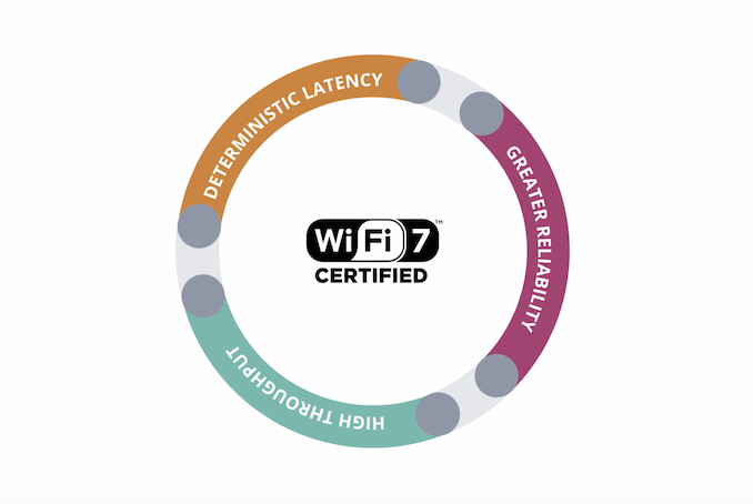
At the 2024 CES, the program was officially announced with products based on silicon from Broadcom, Intel, Mediatek, and Qualcomm obtaining the Wi-Fi CERTIFIED 7 tag. Broadcom, Mediatek, and Qualcomm have already been through two generations of Wi-Fi 7 products, and it is promising to finally see Wi-Fi 7 exit draft status. This enables faster adoption on the client side, as well. The key features of Wi-Fi CERTIFIED 7 are based on the efforts of the IEEE 802.11be EHT (Extremely High Throughput) working group.
The introduction of 6 GHz support in Wi-Fi 6E in select regions opened up channels that were hitherto unavailable for in-home wireless use. Wi-Fi CERTIFIED 7 brings in support for 320 MHz channels. These ultra-wide channels are available only in the 6 GHz band.
These channels are responsible for the high throughput promised in Wi-Fi CERTIFIED 7. However, the non-availability of 6 GHz in many regions has proved to be a deterrent for client device vendors. Many of these companies do not want to spend extra for features that are not available across all geographies. It is likely that many client devices (particularly on the smartphone side) will ship without support for 320 MHz channels initially.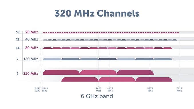
Multi-Link Operation (MLO) is yet another technique to boost available bandwidth for a single client. Wi-Fi CERTIFIED 7 allows clients to connect to the access point through multiple bands at the same time. It also increases the reliability of connections.
Wi-Fi 7 also brings in 4K QAM , allowing up to 12 bits to be encoded per symbol. This represents an increase in spectral efficiency of 20% over Wi-Fi 6 (which only required support for 1024 QAM).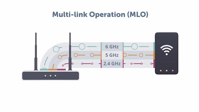
Dense constellations require extremely sophisticated circuitry at both the transmitter (linear power amplifiers) and receiver ends (to avoid symbol decoding without errors). Those are part of the advancements that we can see in Wi-Fi CERTIFIED 7 devices.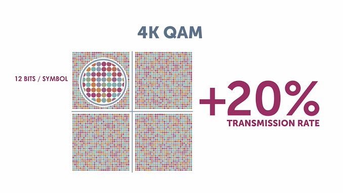
Some of the other key updates in Wi-Fi CERTIFIED 7 include support for 512 compressed block acks, multiple resouce units to a single station / client, and triggered uplink access.
802.11n introduced the concept of block acks at the MAC layer where multiple wireless 'frames' (MAC Protocol Data Units or MPDUs to be more exact) can be acknowledged by the receiver in one response. The ack indicates the missed MPDUs, if any, in the previously transmitted set. In Wi-Fi 6, the limit for the number of MPDUs per block ack was 256. In Wi-Fi 7, this has been pushed up to 512. Spreading out this communication allows for better resource usage.
Wi-Fi 6 introduced the concept of resource units in the OFDMA scheme wherein the radio channel gets partitioned into smaller frequency allocations called RUs. These allow small packets to be transmitted to multiple users at the same time. In Wi-Fi 6, each user could get only ne RU. Wi-Fi 7 allows for better efficiency by allocating non-contiguous RUs to a single user.
Wi-Fi 6 introduced the concept of triggered uplink access, allowing clients to simultaneously transmit data back to the access point in an independent manner. This transmission is synchronized by the AP sending out a trigger frame containing the resource unit allocation information for each client. Wi-Fi 7 optimizes this scheme further for QoS requirements and latency-sensitive streams.
In the meanwhile, the 802.11 working group has already started the ground work for Wi-Fi 8. 802.11bn (extremely high reliability or EHR) aims to bring more resilience to high-speed Wi-Fi networks by allowing multi-link operation distributed over multiple access points, coordination between multiple access points, and power saving features on the access point side.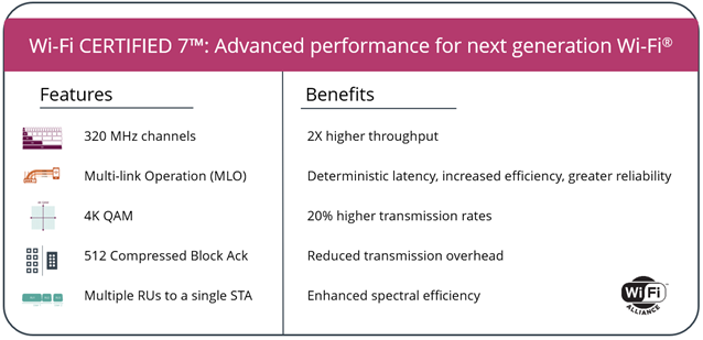
The Wi-Fi Alliance expects a wide range of application scenarios for Wi-Fi 7, now that certification is in place.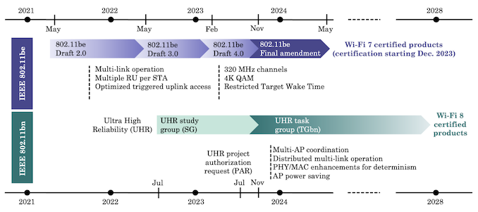
Timeline for 802.11bn (EHR): Wi-Fi 8 Deployments in 2027 - 2028? (Source: What Will Wi-Fi 8 Be? A Primer on IEEE 802.11bn Ultra High Reliability [PDF])
These include mobile gaming, video conferencing, industrial IoT, automotive, multi-user AR / VR / XR, immersive e-training modules, and other use-cases. Wi-Fi 6 brought in a number of technological advancements to Wi-Fi, and Wi-Fi 7 has added to that. Unfortunately, AR / VR / XR has been trying to break into the mainstream for quite some time, but has met with muted success. It is one of the primary single-client use-cases that can benefit from features like MLO in Wi-Fi 7.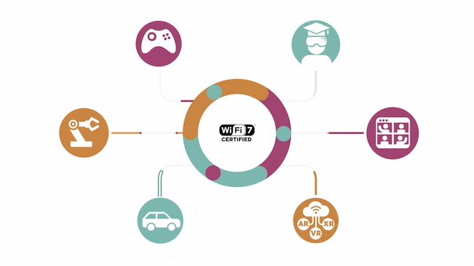
Advancements in spectral efficiency over the last few generations have helped greatly in enterprise deployments. These are scenarios where it is necessary to service a large number of clients with a single access point while maintaining acceptable QoS. User experience in MDUs (multi-dwelling units / apartments) where multiple wireless networks jostle with each other has also improved. That said, vendors are still in search of the ideal single-client scenario to bring out the benefits of Wi-Fi 7 - wireline speeds have largely been stagnant over the last decade, and there are very few ISPs offering gigabit speeds at reasonable prices or over a wide enough area. Both wireline and wireless technologies have to evolve in tandem to bring consumer benefit and pull them in with attractive use-cases. As it currently stands, the pace of progress in Wi-Fi has largely surpassed wired networks over the last couple of decades.
Gallery: Wi-Fi Alliance Introduces Wi-Fi CERTIFIED 7: 802.11be Prepares for Draft Standard Exit


More...
-
01-23-24, 11:31 PM #12007
Anandtech: Update: Samsung Announces 990 EVO SSD, Energy-Efficiency with Dual-Mode PC
After Samsung's earlier product page snafu, the company is officially launching their next-generation mainstream client SSD today. The 990 EVO will be available in both 1TB and 2TB capacities, and offers an interesting mix of both PCIe Gen 5 and PCIe Gen 4 support by allowing up to 2 lanes of PCIe connectivity at Gen 5 speeds, or up to 4 lanes at Gen 4 and below.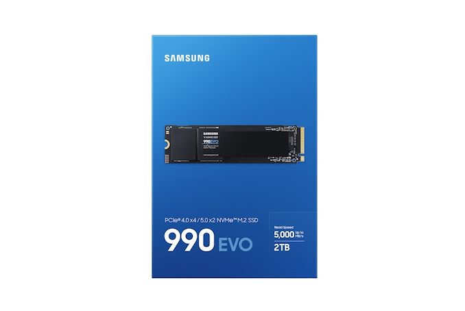
The release of the 990 EVO marks the return of the EVO SSD brand after it was quietly put aside during the 980 generation, when Samsung's sole non-PRO drive was the vanilla 980 SSD. Consequently, Samsung's own performance comparisons for the new drive are against the most recent EVO, the 970 EVO Plus, though similar to how the vanilla 980 was effectively the 970 EVO successor, in many ways this is the successor to the 980.
The drives are available immediately from Samsung. The company has set the retail prices of the drives at $125 for the 1TB model, and $210 for the 2TB. These are stiff prices for a drive debuting in the highly-competitive mainstream SSD market, though admittedly not unusual for a Samsung drive launch.
Our original story (with updated technical specifications) follows as below:
Originally Published: 01/09/2024
Samsung's launch of the 990 EVO M.2 2280 SSD appears to be imminent, as official product pages with specifications went live in certain regions a few days back before getting pulled down.
The most interesting aspect the 990 EVO is not the claimed speeds, but the fact that it can operate in either Gen 4 or Gen 5 modes with different number of lanes. The recently launched mobile platforms from both AMD and Intel use Gen 4 lanes for the storage subsystem. However, with progress in technology it is inevitable that this will move to Gen 5 in the future. In the meanwhile, thermal constraints in mobile systems may prevent notebook manufacturers from going in for desktop Gen 5 speeds (8 - 14 GBps). An attractive option for such cases would be to move to a two-lane Gen 5 implementation that would help in retaining the same Gen 4 x4 bandwidth capability, but cut down on the BOM cost by reducing the number of pins / lane count on the host side. It appears that Samsung's 990 EVO is a platform designed with such a scenario in mind.
PCIe PHYs / controllers have backward compatibility, and the 990 EVO's SSD controller incorporates a 4-lane Gen 5 controller and PHY. During the training phase with the host, both the link bandwidth and lane count can be negotiated. It appears that the SSD is configured to advertise Gen 5 speeds to the host if only two lanes are active.
Samsung appears to be marketing only 1TB and 2TB capacities of the 990 EVO. Based on the product photos online, the models appear to be single-sided units (making them compatible with a wider variety of mobile platforms). The flash packages appear to be 1TB each, and the EVO moniker / advertisement of Host Memory Buffer support / controller package markings in the product photos points to a DRAM-less SSD controller - the Piccolo S4LY022. The quoted performance numbers appear low for a 176L / 236L V-NAND product. TechPowerUp believes that these SSDs are using an updated V6 (133L, termed V6 Prime) with better efficiency and yields compared to the regular V6.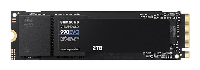
Samsung is also touting much-improved power efficiency, with transfer rates being 2 - 3x per Watt compared to the 970 EVO. The Piccolo controller's 5nm fabrication process and the V6 Prime's efficiency improvements have a significant say in that aspect.Samsung 990 EVO Specifications Capacity 1 TB 2 TB Controller Samsung S4LY022 Piccolo NAND Flash Samsung Updated 6th Gen. V-NAND (133L 3D TLC) Form-Factor, Interface Single-Sided M.2-2280, PCIe 4.0 x4 / 5.0 x2, NVMe 2.0 Sequential Read 5000 MB/s 5000 MB/s Sequential Write 4200 MB/s 4200 MB/s Random Read IOPS 680K 700K Random Write IOPS 800K 800K SLC Caching Yes TCG Opal Encryption Yes Warranty 5 years Write Endurance 600 TBW
0.3 DWPD1200 TBW
0.3 DWPD
Pricing and concrete launch dates for the 990 EVO are not available yet. The delta in specifications for the 1TB and 2TB models will be updated in the table above once the drives are officially announced. The 1TB model is priced at $125 and the 2TB version at $210. Both SKUs are available for purchase today.
More...
-
01-24-24, 05:15 PM #12008
Anandtech: MLCommons To Develop PC Client Version of MLPerf AI Benchmark Suite
MLCommons, the consortium behind the MLPerf family of machine learning benchmarks, is announcing this morning that the organization will be developing a new desktop AI benchmarking suite under the MLPerf banner. Helmed by the body’s newly-formed MLPerf Client working group, the task force will be developing a client AI benchmark suit aimed at traditional desktop PCs, workstations, and laptops. According to the consortium, the first iteration of the MLPerf Client benchmark suite will be based on Meta’s Llama 2 LLM, with an initial focus on assembling a benchmark suite for Windows.
The de facto industry standard benchmark for AI inference and training on servers and HPC systems, MLCommons has slowly been extending the MLPerf family of benchmarks to additional devices over the past several years. This has included assembling benchmarks for mobile devices, and even low-power edge devices. Now, the consortium is setting about covering the “missing middle” of their family of benchmarks with an MLPerf suite designed for PCs and workstations. And while this is far from the group’s first benchmark, it is in some respects their most ambitious effort to date.
The aim of the new MLPerf Client working group will be to develop a benchmark suitable for client PCs – which is to say, a benchmark that is not only sized appropriately for the devices, but is a real-world client AI workload in order to provide useful and meaningful results. Given the cooperative, consensus-based nature of the consortium’s development structure, today’s announcement comes fairly early in the process, as the group is just now getting started on developing the MLPerf Client benchmark. As a result, there are still a number of technical details about the final benchmark suite that need to be hammered out over the coming months, but to kick things off the group has already narrowed down some of the technical aspects of their upcoming benchmark suite.
Perhaps most critically, the working group has already settled on basing the initial version of the MLPerf Client benchmark around Meta's Llama 2 large language model, which is already used in other versions of the MLPerf suite. Specifically, the group is eyeing 7 billion parameter version of that model (Llama-2-7B), as that’s believed to be the most appropriate size and complexity for client PCs (at INT8 precision, the 7B model would require roughly 7GB of RAM). Past that however, the group still needs to determine the specifics of the benchmark, most importantly the tasks which the LLM will be benchmarked executing on.
With the aim of getting it on PCs of all shapes and sizes, from laptops to workstations, the MLPerf Client working group is going straight for mass market adoption by targeting Windows first – a far cry from the *nix-focused benchmarks they’re best known for. To be sure, the group does plan to bring MLPerf Client to additional platforms over time, but their first target is to hit the bulk of the PC market where Windows reigns supreme.
In fact, the focus on client computing is arguably the most ambitious part of the project for a group that already has ample experience with machine learning workloads. Thus far, the other versions of MLPerf have been aimed at device manufacturers, data scientists, and the like – which is to say they’ve been barebones benchmarks. Even the mobile very of the MLPerf benchmark isn’t very accessible to end-users, as it’s distributed as a source-code release intended to be compiled on the target system. The MLPerf Client benchmark for PCs, on the other hand, will be a true client benchmark, distributed as a compiled application with a user-friendly front-end. Which means the MLPerf Client working group is tasked with not only figuring out what the most representative ML workloads will be for a client, but then how to tie that together into a useful graphical benchmark.
Meanwhile, although many of the finer technical points of the MLPerf Client benchmark suite remain to be sorted out, talking to MLCommons representatives, it sounds like the group has a clear direction in mind on the APIs and runtimes that they want the benchmark to run on: all of them. With Windows offering its own machine learning APIs (WinML and DirectML), and then most hardware vendors offering their own optimized platforms on top of that (CUDA, OpenVino, etc), there are numerous possible execution backends for MLPerf Client to target. And, keeping in line with the laissez faire nature of the other MLPerf benchmarks, the expectation is that MLPerf Client will support a full gamut of common and vendor-proprietary backends.
In practice, then, this would be very similar to how other desktop client AI benchmarks work today, such as UL’s Procyon AI benchmark suite, which allows for plugging in to multiple execution backends. The use of different backends does take away a bit from true apples-to-apples testing (though it would always be possible to force fallback to a common API like DirectML), but it gives the hardware vendors room to optimize the execution of the model to their hardware. MLPerf takes the same approach to their other benchmarks right now, essentially giving hardware vendors free reign to come up with new optimizations – including reduced precision and quantization – so long as they don’t lose inference accuracy and fail meet the benchmark’s overall accuracy requirements.
Even the type of hardware used to execute the benchmark is open to change: while the benchmark is clearly aimed at leveraging the new field of NPUs, vendors are also free to run it on GPUs and CPUs as they see fit. So MLPerf Client will not exclusively be an NPU or GPU benchmark.
Otherwise, keeping everyone on equal footing, the working group itself is a who’s who of hardware and software vendors. The list includes not only Intel, AMD, and NVIDIA, but Arm, Qualcomm, Microsoft, Dell, and others. So there is buy-in from all of the major industry players (at least in the Windows space), which has been critical for driving the acceptance of MLPerf for servers, and will similarly be needed to drive acceptance of MLPerf client.
The MLPerf Client benchmark itself is still quite some time from release, but once it’s out, it will be joining the current front-runners of UL’s Procyon AI benchmark and Primate Labs’ Geekbench ML, both of which already offer Windows client AI benchmarks. And while benchmark development is not necessarily a competitive field, MLCommons is hoping that their open, collaborative approach will be something that sets them apart from existing benchmarks. The nature of the consortium means that every member gets a say (and a vote) on matters, which isn’t the case for proprietary benchmarks. But it also means the group needs a complete consensus in order to move forward.
Ultimately, the initial version of the MLPerf Client benchmark is being devised as more of a beginning than an end product in and of itself. Besides expanding the benchmark to additional platforms beyond Windows, the working group will also eventually be looking at additional workloads to add to the suite – and, presumably, adding more models beyond Llama 2. So while the group has a good deal of work ahead of them just to get the initial benchmark out, the plan is for MLPerf Client to be long-lived, long-supported benchmark as the other MLPerf benchmarks are today.
More...
-
01-24-24, 05:15 PM #12009
Anandtech: Asus Launches USB4 Add-In-Card: Two 40 Gbps Ports for Desktops
Asus has introduced a USB4 PCIe add-in-card for the company's desktop motherboards, allowing users to add two USB4 ports to their systems. The card can be used to connect up to four devices and a display to each of its ports, and can even be used to charge laptops that support USB charging.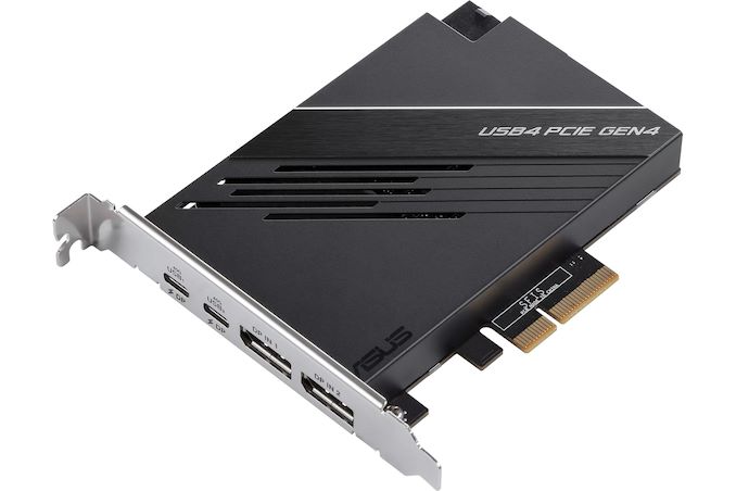
The Asus USB4 PCIe Gen4 Card is based on ASMedia's ASM4242 controller and supports two USB4 ports at 40 Gbps data rates, with up to 60W USB Power Delivery. The board also has two DisplayPort inputs to in order to route graphics through the card as well in order to make full use of the versatility offered by USB4 and the Type-C cable. Alternatively, one can connect the card to the motherboard TB3/TB4 header and use integrated GPU to handle displays connected using USB-C cables.
One of the main advantages that the ports of Asus USB4 PCIe Gen4 card have over USB4 ports found on some motherboards is that it supports 60W Quick Charge 4+ to devices, which enables to charge laptops or connect devices that demand more than 15W of power (but less than 60W).
There is a catch about the Asus USB4 PCIe Gen4 card though: it is only compatible with Asus motherboards and needs a motherboard with a Thunderbolt or USB4 header (which is mostly designed to use integrated GPU). The company says that many of its AM5 and Intel 700-based motherboards have an appropriate header, so the device can be used on most of its current-generation boards.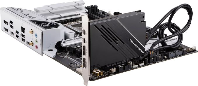
The card operates on a PCIe 4.0 x4 interface, providing 7.877 GB/s of bandwidth to the ASMedia controller. The card also features a six-pin auxiliary PCIe connector to supply the additional power needed for the card's high-powered ports.
Asus has yet to reveal recommended price and availability date of its USB4 expansion card. Given that this is not the industry's first card of this kind, expect it to be competitively priced in comparison to existing Thunderbolt 3/4 expansion cards, which have been on the market for a while.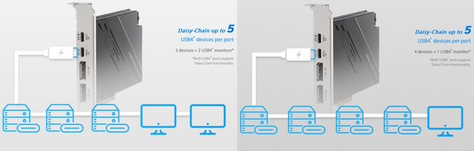
More...
-
01-25-24, 07:18 PM #12010
Anandtech: Intel Teams Up with UMC for 12nm Fab Node at IFS
Intel and UMC on Thursday said they had entered into an agreement to jointly to develop a 12 nm photolithography process for high-growth markets such as mobile, communication infrastructure, and networking. Under the terms of the deal, the two companies will co-design a 12 nm-class foundry node that Intel Foundry Services (IFS) will use at its fabs in Arizona to produce a variety of chips.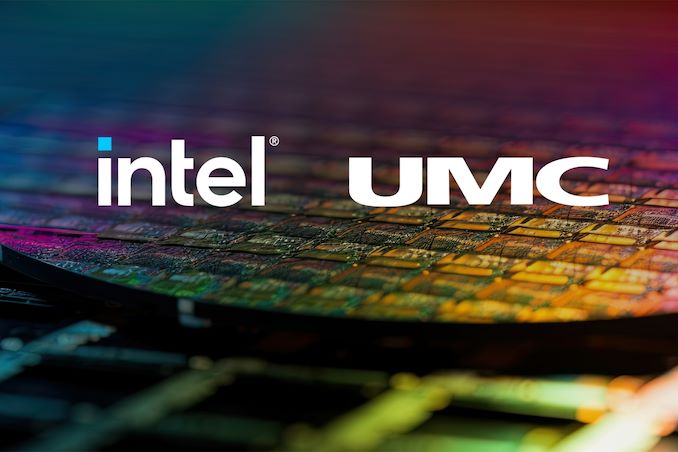
The new 12 nm manufacturing process will be developed in Arizona and used in Fabs 12, 22, and 32 at Intel's Ocotillo Technology Fabrication site in Arizona. The two companies will jointly work on the fabrication technology itself, process design kit (PDK), electronic design automation (EDA) tools, and intellectual properties (IP) solutions from ecosystem partners to enable quick deployment of the node by customers once the tech is production ready in 2027.
Intel's Fabs 12, 22, and 32 in Arizona are currently capable of making chips on Intel's 7nm-class, 10 nm, 14 nm, and 22 nm manufacturing processes. So as Intel rolls out its Intel 4, Intel 3, and Intel 20A/18A production at other sites and winds down production of Intel 7-based products, these Arizona fabs will be freed to produce chips on a variety of legacy and low-cost nodes, including the 12 nm fabrication process co-developed by UMC and Intel.
While Intel itself has a variety of highly-customized process technologies for internal use to produce its own CPUs and similar products, its IFS division essentially has only three: Intel 16 for cost-conscientious customers designing inexpensive low-power products (including those with RF support), Intel 3 for those who develop high-performance solutions yet want to stick to familiar FinFET transistors, and Intel 18A aimed at developers seeking for no-compromise performance and transistor density enabled by gate-all-around RibbonFET transistors and PowerVia backside power delivery. To be a major foundry player, three process technologies are not enough; IFS needs to address as many customers as possible, and this is where collaboration with UMC comes into play.
UMC already has hundreds of customers who develop a variety of products for automotive, consumer electronics, Internet-of-Things, smartphone, storage, and similar verticals. Those customers are quite used to working with UMC, but the best technology that the foundry has is its 14 nm-class 14FFC node. By co-designing a 12 nm-class process technology with Intel, UMC will be able to address customers who need something more advanced than its own 14 nm node, but without having to develop an all-new manufacturing process itself and procuring advanced fabs tools. Meanwhile, Intel gains customers for its fully depreciated (and presumably underutilized) fabs.
The collaboration on a 12 nm node extends the process technology offerings for both companies. What remains to be seen is whether Intel's own 16 nm-class process technology will compete and/or overlap with the jointly developed 12 nm node. To avoid this, we would expect UMC to add some of its know-how to the new tech and make it easier for customers to migrate to this process from its 28 nm-class and 14FFC offerings, which guarantees that the 12 nm node will be used for years to come.
Intel's partnership with UMC comes on the heels of the company's plan to build 65nm chips for Tower Semiconductor at its Fab 11X. Essentially, both collaborations allow Intel's IFS to use its fully depreciated fabs, gain relationship with fabless chip designers, and earn money. Meanwhile, its partners expand their capacity and reach without making heavy capital investments.
"Our collaboration with Intel on a U.S.-manufactured 12 nm process with FinFET capabilities is a step forward in advancing our strategy of pursuing cost-efficient capacity expansion and technology node advancement in continuing our commitment to customers," said Jason Wang, UMC co-president. "This effort will enable our customers to smoothly migrate to this critical new node, and also benefit from the resiliency of an added Western footprint. We are excited for this strategic collaboration with Intel, which broadens our addressable market and significantly accelerates our development roadmap leveraging the complementary strengths of both companies."
More...


 Quote
Quote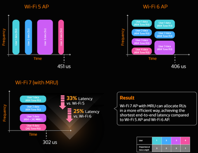
Thread Information
Users Browsing this Thread
There are currently 26 users browsing this thread. (0 members and 26 guests)


Bookmarks