

Results 12,091 to 12,100 of 12103
Thread: Anandtech News
-
07-03-24, 08:12 PM #12091
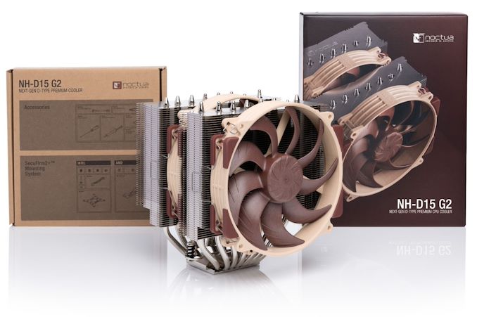
Anandtech: Noctua Launches New Flagship Cooler: NH-D15 G2 with LGA1851 CPUs Support
On Tuesday, Noctua introduced its second-generation NH-D15 cooler, which offers refined performance and formally supports Intel's next-generation Arrow Lake-S processors in LGA1851 packaging. Alongside its NH-D15 G2 CPU cooler, Noctua also introduced its NF-A14x25r G2 140mm fans.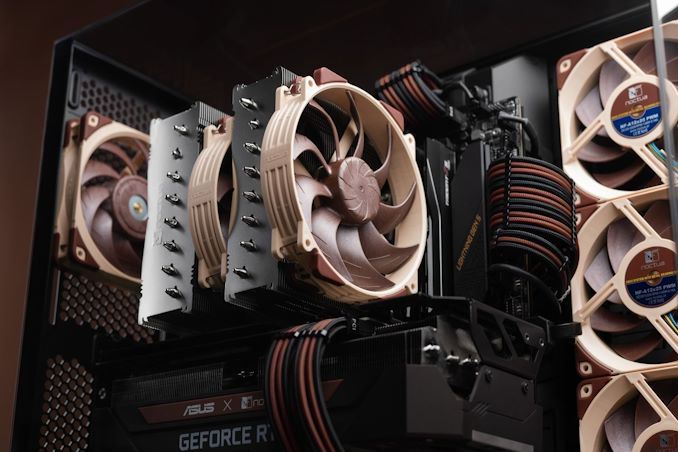
The Noctua NH-D15 G2 is an enhanced version of the popular NH-D15 cooler with eight heat pipes, two asymmetrical fin-stack and two speed-offset 140-mm PWM fans (to avoid acoustic interaction phenomena such as periodic humming or intermittent vibrations). According to the manufacturer, these key components are tailored to work efficiently together to deliver superior quiet cooling performance, rivalling many all-in-one water cooling systems and pushing the boundaries of air cooling efficiency.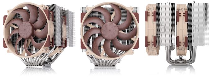
Noctua offers the NH-D15 G2 in three versions to address the specific requirements of modern CPUs. The regular version is versatile and can be used for AMD's AM5 processors and Intel's LGA1700 CPUs with included mounting accessories. The HBC (High Base Convexity) variant is tailored for LGA1700 processors, especially those subjected to full ILM pressure or those that have deformed over time, ensuring excellent contact quality despite the concave shape of the CPU. Finally, the LBC (Low Base Convexity) version is tailored for flat rectangular CPUs, providing optimal contact on AMD's AM5 and other similar processors.
While there are three versions of NH-D15 G2 aimed at different processors, they are all said to be compatible with a wide range of motherboards and other hardware. The new coolers' offset construction ensures clearance for the top PCIe x16 slot on most current motherboards. Additionally, they feature the upgraded Torx-based SecuFirm2+ multi-socket mounting system and come with Noctua's NT-H2 thermal compound.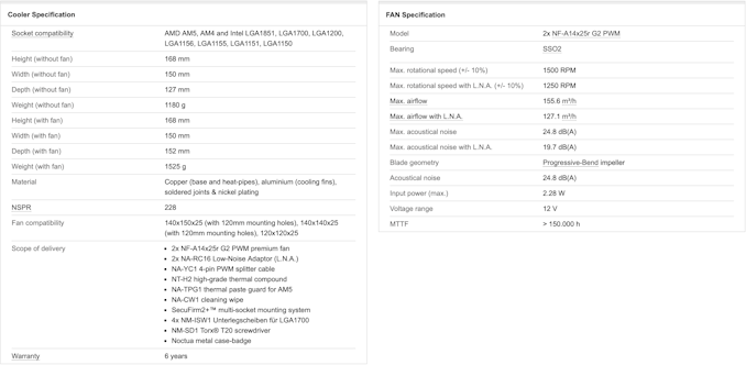
For those looking to upgrade existing coolers like the NH-D15, NH-D15S, or NH-U14S series, Noctua is also releasing the NF-A14x25r G2 fans separately. These round-frame fans are fine-tuned in single and dual fan packages to minimize noise levels while offering decent cooling performance.
Finally, Noctua is also prepping a square-frame version of the NF-A14x25 G2 fan for release in September. This variant targets water-cooling radiators and case-cooling applications and promises to extend the versatility of Noctua's cooling solutions further.
All versions of Noctua's NH-D15 G2 coolers cost $149.90/€149.90. One NF-A14x25 G2 fan costs $39.90/€39.90, whereas a package of two fans costs $79.80/€79.80. The cooler is backed with a six-year warranty.
More...
-
07-05-24, 08:44 AM #12092
Anandtech: The Lian Li EDGE EG1000 1000W ATX 3.1 PSU Review: Power On The Edge
Lian Li Industrial Co., Ltd., established in 1983, is a Taiwanese company specializing in the manufacture of computer cases, power supplies, and accessories. They are one of the oldest players in the PC market and are known for their focus on aluminum-based designs. Lian Li produces a range of products aimed at both consumer and industrial markets, with the company's offerings including mid-tower and full-tower cases and more compact cases for smaller builds. Amongst consumers and PC enthusiasts, Lian Li's products are recognized for their build quality, modularity, and innovative features, catering to a diverse set of needs in the PC building community.
This review focuses on the latest addition to Lian Li's PSU lineup: the EG1000 Platinum ATX 3.1 PSU. This power supply unit partially complies with the ATX 3.1 design guide (the paragraphs related to electrical quality and performance). It is designed to meet the demanding requirements of modern gaming PCs, with its specifications indicating good efficiency and robust power delivery. Featuring fully modular cables with individually sleeved wires, dynamic fan control for optimal cooling, and advanced internal topologies, the EG1000 Platinum aims to provide both reliability and performance. However, behind its long list of features, the highlight of the EG1000 Platinum is the shape of the chassis itself, which forgoes the ATX cuboid shape and standard length.
More...
-
07-05-24, 08:44 AM #12093
Anandtech: Kioxia's High-Performance 3D QLC NAND Enables High-End High-Capacity SSDs
This week, Kioxia introduced its new 3D QLC NAND devices aimed at high-performance, high-capacity drives that could redefine what we typically expect from QLC-based SSDs. The components are 1 Tb and 2 Tb 3D QLC NAND ICs with a 3600 MT/s interface speed that could enable M.2-2230 SSDs with a 4 TB capacity and decent performance.
Kioxia's 1 Tb (128 MB) and 2 Tb (256 TB) 3D QLC NAND devices are made on the company's BICS 8 process technology and feature 238 active layers as well as CMOS directly Bonded to Array (CBA) design, which implies that CMOS (including interface and buffers circuitry) is built on a specialized node and bonded to the memory array. Such a manufacturing process enabled Kioxia (and its manufacturing partner Western Digital) to achieve a particularly high interface speed of 3600 MT/s.
In addition to being one of the industry's first 2 Tb QLC NAND devices, the component features a 70% higher write power efficiency compared to Kioxia's BICS 5 3D QLC NAND devices, which is a bit vague statement as the new ICs have higher capacity and performance in general. This feature will be valuable for data centre applications, though I do not expect someone to use 3D QLC memory for write-intensive applications in general. Yet, these devices will be just what the doctor ordered for AI: read-intensive, content distribution, and backup storage.
It is interesting to note that Kioxia's 1 Tb 3D QLC NAND, optimized for performance, has a 30% faster sequential write performance and a 15% lower read latency than the 2 Tb 3D QLC component. These qualities (alongside a 3600 MT/s interface) promise to make Kioxia's 1 Tb 3D QLC competitive even for higher-end PCIe Gen5 x4 SSDs, which currently exclusively use 3D TLC memory.
The remarkable storage density of Kioxia's 2Tb 3D QLC NAND devices will allow customers to create high-capacity SSDs in compact form factors. For instance, a 16-Hi stacked package (measuring 11.5 mm × 13.5 mm × 1.5 mm) can be used to build a 4TB M.2-2230 drive or a 16TB M.2-2280 drive. Even a single 16-Hi package could be enough to build a particularly fast client SSD.
Kioxia is now sampling its 2 Tb 3D QLC NAND BiCS 8 memory with customers, such as Pure Storage.
"We have a long-standing relationship with Kioxia and are delighted to incorporate their eighth-generation BiCS Flash 2Tb QLC flash memory products to enhance the performance and efficiency of our all-flash storage solutions," said Charles Giancarlo, CEO of Pure Storage. "Pure's unified all-flash data storage platform is able to meet the demanding needs of artificial intelligence as well as the aggressive costs of backup storage. Backed by Kioxia technology, Pure Storage will continue to offer unmatched performance, power efficiency, and reliability, delivering exceptional value to our customers."
"We are pleased to be shipping samples of our new 2Tb QLC with the new eighth-generation BiCS flash technology," said Hideshi Miyajima, CTO of Kioxia. "With its industry-leading high bit density, high speed data transfer, and superior power efficiency, the 2Tb QLC product will offer new value for rapidly emerging AI applications and large storage applications demanding power and space savings."
There is no word on when the 1 Tb 3D QLC BiCS 8 memory will be sampled or released to the market.
More...
-
07-05-24, 04:19 PM #12094
Anandtech: Samsung Joins The 60 TB SSD Club, Looking Forward To 120 TB Drives
Multiple companies offer high-capacity SSDs, but until recently, only two companies offered high-performance 60 TB-class drives with a PCIe interface: Solidigm and Western Digital. As our colleagues from Blocks & Files discovered, Samsung quietly rolled out its BM1743 61.44 TB solid-state drive in mid-June and now envisions 120 TB-class SSDs based on the same platform.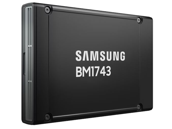
Samsung's BM1743 61.44 TB features a proprietary controller and relies on Samsung's 7th Generation V-NAND (3D NAND) QLC memory. Moreover, Samsung believes that its 7th Gen V-NAND 'has the potential to accommodate up to 122.88 TB,'
Samsung plans to offer the BM1743 in two form factors: U.2 for PCIe 4.0 x4 to address traditional servers and E3.S for PCIe 5.0 x4 interfaces to address machines designed to offer maximum storage density. BM1743 can address various applications, including AI training and inference, content delivery networks, and read-intensive workloads. To that end, its write endurance is 0.26 drive writes per day (DWPD) over five years.
Regarding performance, Samsung's BM1743 is hardly a champion compared to high-end drives for gaming machines and workstations. The drive can sustainably achieve sequential read speeds of 7,200 MB/s and write speeds of 2,000 MB/s. It can handle up to 1.6 million 4K random reads and 110,000 4K random writes for random operations.
Power consumption details for the BM1743 have not been disclosed, though it is expected to be high. Meanwhile, the drive's key selling point is its massive storage density, which likely outweighs concerns over its absolute power efficiency for intended applications, as a 60 TB SSD still consumes less than multiple storage devices offering similar capacity and performance.
As noted above, Samsung's BM1743 61.44 TB faces limited competition in the market, so its price will be quite high. For example, Solidigm's D5-P5336 61.44 TB SSD costs $6,905. Other companies, such as Kioxia, Micron, and SK Hynix, have not yet introduced their 60TB-class SSDs, which gives Samsung and Solidigm an edge for now.
More...
-
07-12-24, 01:32 PM #12095
Anandtech: Applied Materials' New Deposition Tool Enables Copper Wires to Be Used for
Although the pace of Moore's Law has undeniably slackened in the last decade, transistor density is still increasing with every new process technology. But there is a challenge with feeding power to smaller transistors, as with the smaller transistors comes thinner power wires within the chip, which increases their resistance and may cause yield loss. Looking to combat that effect, this week Applied Materials introduced its new Applied Endura Copper Barrier Seed IMS with Volta Ruthenium Copper Vapor Deposition (CVD) tool, which enables chipmakers to keep using copper for wiring with 2 nm-class and more advanced process technologies.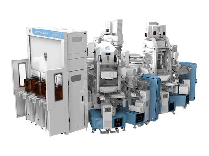
Today's advanced logic processors have about 20 layers of metal, with thin signal wires and thicker power wires. Scaling down wiring with shrinking transistors presents numerous challenges. Thinner wires have higher electrical resistance, while closer wires heighten capacitance and electrical crosstalk. The combination of the two can lead to increased power consumption while also limiting performance scaling, which is particularly problematic for datacenter grade processors that are looking to have it all. Moving power rails to a wafer's back-side is expected to enhance performance and efficiency by reducing wiring complexity and freeing up space for more transistors.
But backside power delivery network (BSPDN) does not solve the problem with thin wires in general. As lithographic scaling progresses, both transistor features and wiring trenches become smaller. This reduction means that barriers and liners take up more space in these trenches, leaving insufficient room to deposit copper without creating voids, which raises resistance and can lower yields. Additionally, the closer proximity of wires thins the low-k dielectrics, making them more vulnerable to damage during the etching process. This damage increases capacitance and weakens the chips, making them unsuitable for 3D stacking. Consequently, as the industry advances, copper wiring faces significant physical scaling challenges. But Applied Materials has a solution.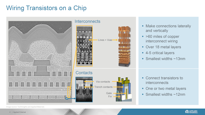
Adopting Binary RuCo Liners
Contemporary manufacturing technologies use reflow to fill interconnects with copper, where anneals help the copper flow from the wafer surface into wiring trenches and vias. This process depends on the liners on which the copper flows. Normally, a CVD cobalt film was used for liners, but this film is too thick for 3nm-class nodes (which would affect resistance and yield).
Applied Materials proposes using a ruthenium cobalt (RuCo) binary liner with a thickness under 20A (2nm, 20 angstroms), which would provide better surface properties for copper reflow. This would ultimately allow for 33% more space for void-free conductive copper to be reflowed, reducing the overall resistance by 25%. While usage of the new liner requires new tooling, it can enable better interconnects that mean higher performance, lower power consumption and higher yields.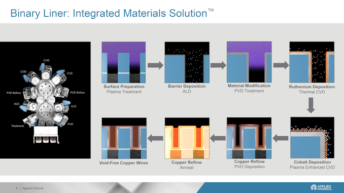
Gallery: Applied Materials New Tool Enables Copper Wires to Be Used for 2nm and Beyond


Applied Materials says that so far its new Endura Copper Barrier Seed IMS with Volta Ruthenium CVD tool has been adopted by all leading logic makers, including TSMC and Samsung Foundry for their 3nm-class nodes and beyond.
"The semiconductor industry must deliver dramatic improvements in energy-efficient performance to enable sustainable growth in AI computing," said Dr. Y.J. Mii, Executive Vice President and Co-Chief Operating Officer at TSMC. "New materials that reduce interconnect resistance will play an important role in the semiconductor industry, alongside other innovations to improve overall system performance and power."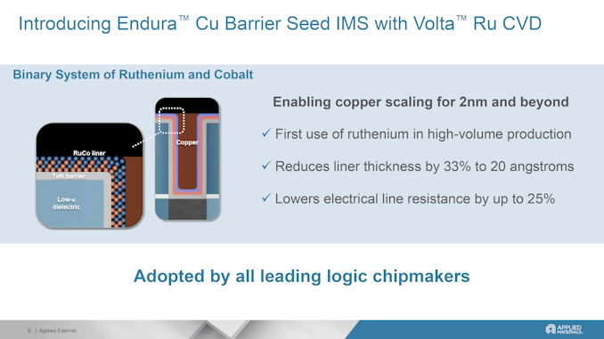
New Low-K Dielectric
But thin and efficient liner is not the only thing crucial for wiring at 3nm production nodes and beyond. Trenches for wiring are filed not only with a Co/RuCo liner and a Ta/N barrier, but with low dielectric constant (Low-K) film to minimize electrical charge buildup, reduce power consumption, and lower signal interference. Applied Materials has offered its Black Diamond Low-K film since the early 2000s.
But new production nodes require better dielectrics, so this week the company introduced an upgraded version of Black Diamond material and a plasma-enhanced chemical vapor deposition (PEVCD) tool to apply it, the Producer Black Diamond PECVD series. This new material allows for scaling down to 2nm and beyond by further reducing the dielectric constant while also increasing the mechanical strength of the chips, which is good for 3D stacking both for logic and memory. The new Black Diamond is being rapidly adopted by major logic and DRAM chipmakers, Applied says.
"The AI era needs more energy-efficient computing, and chip wiring and stacking are critical to performance and power consumption," said Dr. Prabu Raja, President of the Semiconductor Products Group at Applied Materials. "Applied's newest integrated materials solution enables the industry to scale low-resistance copper wiring to the emerging angstrom nodes, while our latest low-k dielectric material simultaneously reduces capacitance and strengthens chips to take 3D stacking to new heights."
Sources: Applied Materials (1, 2)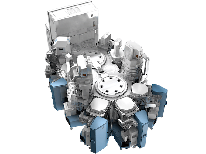
More...
-
07-12-24, 08:03 PM #12096
Anandtech: Troubled AI Processor Developer Graphcore Finds a Buyer: SoftBank
After months of searching for a buyer, troubled U.K.-based AI processor designer Graphcore said on Friday that it has been acquired by SoftBank. The company will operate as a wholly owned subsidiary of SoftBank and will possibly collaborate with Arm, but what remains to be seen what happens to the unique architecture of Graphcore's intelligence processing units (IPUs).
Graphcore will retain its name as it will become a wholly owned subsidiary of SoftBank, which paid either $400 million (according to EE Times) or $500 million (according to BBC) for the company. Over its lifetime, Graphcore has received a total of $700 million of investments from Microsoft and Sequoia Capital, and at its peak in late 2020, was valued at $2.8 billion. Nigel Toon will remain at the helm of Graphcore, which will hire new staff in its UK offices and continue to be headquartered in Bristol, with additional offices in Cambridge, London, Gdansk (Poland), and Hsinchu (China).
"This is a tremendous endorsement of our team and their ability to build truly transformative AI technologies at scale, as well as a great outcome for our company," said Nigel Toon. "Demand for AI compute is vast and continues to grow. There remains much to do to improve efficiency, resilience, and computational power to unlock the full potential of AI. In SoftBank, we have a partner that can enable the Graphcore team to redefine the landscape for AI technology."
Although Graphcore says that it had won contracts with major high-tech companies and deployed its IPUs, it could not compete against NVIDIA and other prêt-à-porter AI processor vendors due to insufficient funding. In the recent years the company's problems were so severe that it had to lay off 20% of its staff, bringing its headcount to around 500. Those cuts also saw office closures in Norway, Japan, and South Korea, which made it even harder to compete against big players.
Graphcore certainly hopes that with SoftBank's deep pockets and willingness to invest in AI technologies in general and AI processors in particular, it will finally be able to compete head-to-head with established players like NVIDIA.
When asked whether Graphcore will work with SoftBank's Arm, Nigel Toon said that he was looking forward to work with all companies controlled by its parent, including Arm. Meanwhile, SoftBank itself is reportedly looking forward to build its own AI processor venture called Project Izanagi to compete against NVIDIA, whereas Arm is reportedly developing AI processors that will work in datacenters owned by SoftBank. Therefore, it remains to be seen where does Graphcore fit in.
For now, the best processor that Graphcore has is its Colossus MK2 IPU, which is built using 59.4 billion transistors and packs in 1,472 independent cores with simultaneous multithreading (SMT) capable of handling 8,832 parallel threads. Instead of using HBM or other types of external memory, the chip integrates 900 MB of SRAM, providing an aggregated bandwidth of 47.5 TB/s per chip. Additionally, it features 10 IPU links to scale with other MK2 processors. When it comes to performance, the MK2 C600 delivers 560 TFLOPS FP8, 280 TFLOPS FP16, and 70 TFLOPS of FP32 performance at 185W. To put the numbers into context, NVIDIA's A100 delivers 312 FP16 TFLOPS without sparsity as well as 19.5 FP32 TFLOPS, whereas NVIDIA's H100 card offers 3,341 FP8 TFLOPS.
Sources: Graphcore, EE Times, BBC, Reuters
More...
-
07-15-24, 09:32 PM #12097
Anandtech: The AMD Zen 5 Microarchitecture: Powering Ryzen AI 300 Series For Mobile a
Back at Computex 2024, AMD unveiled their highly anticipated Zen 5 CPU microarchitecture during AMD CEO Dr. Lisa Su's opening keynote. AMD announced not one but two new client platforms that will utilize the latest Zen 5 cores. This includes AMD's latest AI PC-focused chip family for the laptop market, the Ryzen AI 300 series. In comparison, the Ryzen 9000 series caters to the desktop market, which uses the preexisting AM5 platform.
Built around the new Zen 5 CPU microarchitecture with some fundamental improvements to both graphics and AI performance, the Ryzen AI 300 series, code-named Strix Point, is set to deliver improvements in several areas. The Ryzen AI 300 series looks set to add another footnote in the march towards the AI PC with its mobile SoC featuring a new XDNA 2 NPU, from which AMD promises 50 TOPS of performance. AMD has also upgraded the integrated graphics with the RDNA 3.5, which is designed to replace the last generation of RDNA 3 mobile graphics, for better performance in games than we've seen before.
Further to this, during AMD's recent Tech Day last week, AMD disclosed some of the technical details regarding Zen 5, which also covers a number of key elements under the hood on both the Ryzen AI 300 and the Ryzen 9000 series. On paper, the Zen 5 architecture looks quite a big step up compared to Zen 4, with the key component driving Zen 5 forward through higher instructions per cycle than its predecessor, which is something AMD has managed to do consistently from Zen to Zen 2, Zen 3, Zen 4, and now Zen 5.
More...
-
07-16-24, 03:47 PM #12098
Anandtech: Micron Expands Datacenter DRAM Portfolio with MR-DIMMs
The compute market has always been hungry for memory bandwidth, particularly for high-performance applications in servers and datacenters. In recent years, the explosion in core counts per socket has further accentuated this need. Despite progress in DDR speeds, the available bandwidth per core has unfortunately not seen a corresponding scaling.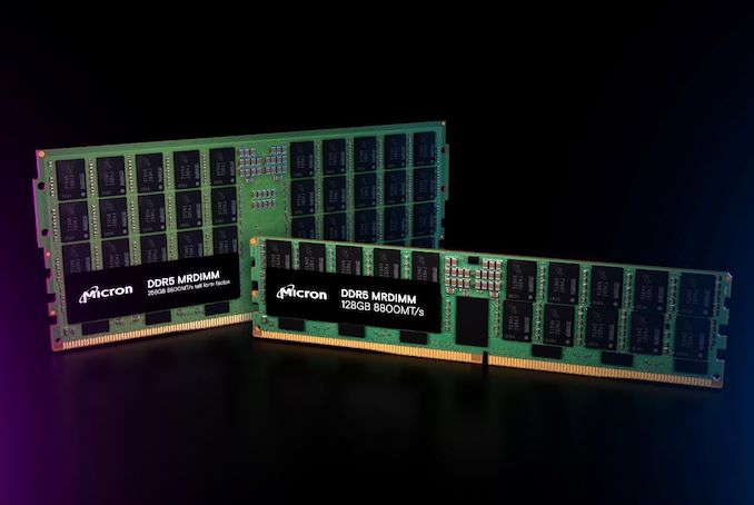
The stakeholders in the industry have been attempting to address this by building additional technology on top of existing widely-adopted memory standards. With DDR5, there are currently two technologies attempting to increase the peak bandwidth beyond the official speeds. In late 2022, SK hynix introduced MCR-DIMMs meant for operating with specific Intel server platforms. On the other hand, JEDEC - the standards-setting body - also developed specifications for MR-DIMMs with a similar approach. Both of them build upon existing DDR5 technologies by attempting to combine multiple ranks to improve peak bandwidth and latency.
How MR-DIMMs Work
The MR-DIMM standard is conceptually simple - there are multiple ranks of memory modules operating at standard DDR5 speeds with a data buffer in front. The buffer operates at 2x the speed on the host interface side, allowing for essentially double the transfer rates. The challenges obviously lie in being able to operate the logic in the host memory controller at the higher speed and keeping the power consumption / thermals in check.
The first version of the JEDEC MR-DIMM standard specifies speeds of 8800 MT/s, with the next generation at 12800 MT/s. JEDEC also has a clear roadmap for this technology, keeping it in sync with the the improvements in the DDR5 standard.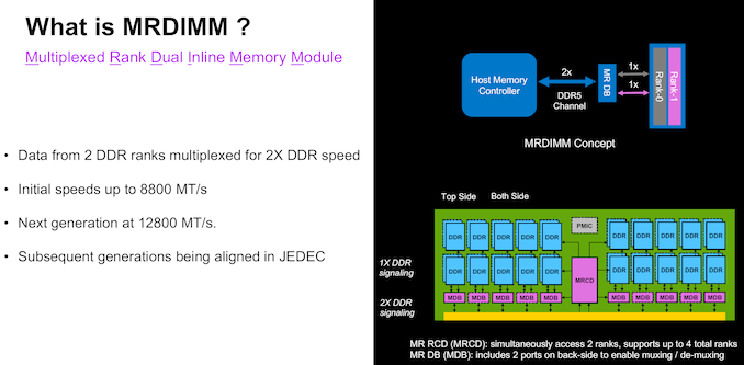
Micron MR-DIMMs - Bandwidth and Capacity Plays
Micron and Intel have been working closely in the last few quarters to bring their former's first-generation MR-DIMM lineup to the market. Intel's Xeon 6 Family with P-Cores (Granite Rapids) is the first platform to bring MR-DIMM support at 8800 MT/s on the host side. Micron's standard-sized MR-DIMMs (suitable for 1U servers) and TFF (tall form-factor) MR-DIMMs (for 2U+ servers) have been qualified for use with the same.
The benefits offered by MR-DIMMs are evident from the JEDEC specifications, allowing for increased data rates and system bandwidth, with improvements in latency. On the capacity side, allowing for additional ranks on the modules has enabled Micron to offer a 256 GB capacity point. It must be noted that some vendors are also using TSV (through-silicon vias) technology to to increase the per-package capacity at standard DDR5 speeds, but this adds additional cost and complexity that are largely absent in the MR-DIMM manufacturing process.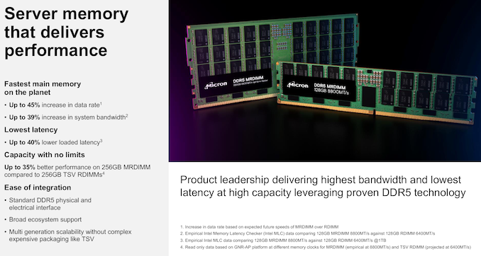
The tall form-factor (TFF) MR-DIMMs have a larger surface area compared to the standard-sized ones. For the same airflow configuration, this allows the DIMM to have a better thermal profile. This provides benefits for energy efficiency as well by reducing the possibility of thermal throttling.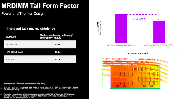
Micron is launching a comprehensive lineup of MR-DIMMs in both standard and tall form-factors today, with multiple DRAM densities and speed options as noted above.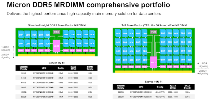
MRDIMM Benefits - Intel Granite Rapids Gets a Performance Boost
Micron and Intel hosted a media / analyst briefing recently to demonstrate the benefits of MR-DIMMs for Xeon 6 with P-Cores (Granite Rapids). Using a 2P configuration with 96-core Xeon 6 processors, benchmarks for different workloads were processed with both 8800 MT/s MR-DIMMs and 6400 MT/s RDIMMs. The chosen workloads are particularly notorious for being limited in performance by memory bandwidth.
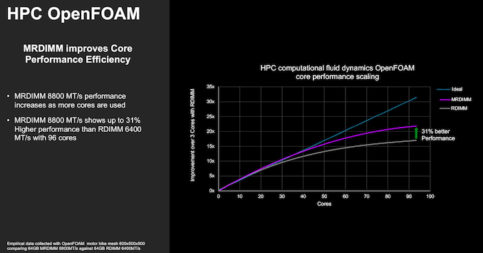
OpenFOAM is a widely-used CFD workload that benefits from MR-DIMMs. For the same memory capacity, the 8800 MT/s MR-DIMM shows a 1.31x speedup based on higher average bandwidth and IPC improvements, along with lower last-level cache miss latency.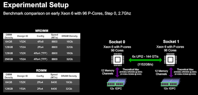
The performance benefits are particularly evident with more cores participating the workload.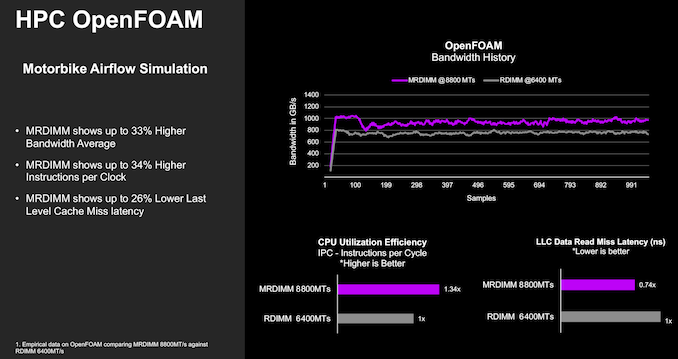
Apache Spark is a commonly used big-data platform operating on large datasets. Depending on the exact dataset in the picture, the performance benefits of MR-DIMMs can vary. Micron and Intel used a 2.4TB set from Intel's Hibench benchmark suite for this benchmark, showing a 1.2x speedup at the same capacity and 1.7x speedup with doubled-capacity TFF MR-DIMMs.
Avoiding the need to push data back to the permanent storage also contributes to the speedup.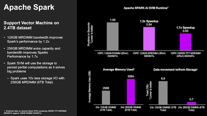
The higher speed offered by MR-DIMMs also helps in AI inferencing workloads, with Micron and Intel showing a 1.31x inference performance improvement along with reduced time to first token for a Llama 3 8B parameter model. Obviously, purpose-built inferencing solutions based on accelerators will perform better. However, this was offered as a demonstration of the type of CPU workloads that can benefit from MR-DIMMs.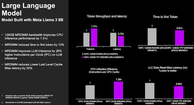
As the adage goes, there is no free lunch. At 8800 MT/s, MR-DIMMs are definitely going to guzzle more power compared to 6400 MT/s RDIMMs. However, the faster completion of workloads mean that the the energy consumption for a given workload will be lower for the MR-DIMM configurations. We would have liked Micron and Intel to quantify this aspect for the benchmarks presented in the demonstration. Additionally, Micron indicated that the energy efficiency (in terms of pico-joules per bit transferred) is largely similar for both the 6400 MT/s RDIMMs and 8800 MT/s MR-DIMMs.
Key Takeaways
The standardization of MR-DIMMs by JEDEC allows multiple industry stakeholders to participate in the market. Customers are not vendor-locked and can compare and contrast options from different vendors to choose the best fit for their needs.
At Computex, we saw MR-DIMMs from ADATA on display. As a Tier-2 vendor without its own DRAM fab, ADATA's play is on cost benefits with the possibility of the DRAM die being sourced from different fabs. The MR-DIMM board layout is dictated by JEDEC specifications, and this allows Tier-2 vendors to have their own play with pricing flexibility. Modules are also built based on customer orders. Micron, on the other hand, has a more comprehensive portfolio / lineup of SKUs for different use-cases with the pros and cons of vertical integration in the picture.
Micron is also not the first to publicly announce MR-DIMM sampling. Samsung announced their own lineup (based on 16Gb DRAM dies) last month. It must be noted that Micron's MR-DIMM portfolio uses 16 Gb, 24 Gb, and 32 Gb dies fabricated in 1β technology. While Samsung's process for the 16 Gb dies used in their MR-DIMMs is not known, Micron believes that their MR-DIMM technology will provide better power efficiency compared to the competition while also offering customers a wider range of capacities and configurations.
More...
-
07-16-24, 11:04 PM #12099
Anandtech: Western Digital Adds 8TB Model to Popular High-End SN850X SSD Drive Family
Western Digital has quietly introduced an 8 TB version of its high-end SN850X SSD, doubling the top capacity of the well-regarded drive family. The new drive offers performance on par with other members of the range, but with twice as much capacity as the previous top-end model – and with a sizable price premium to go with its newfound capacity.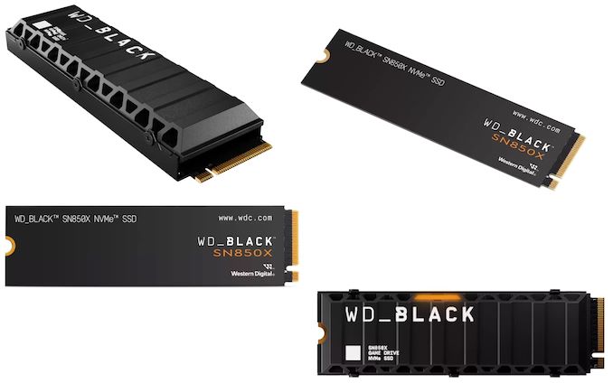
Western Digital introduced its WD_Black SN850X SSDs in the summer of 2022, releasing single-sided 1 TB and 2 TB models, along with a double-sided 4 TB model. But now almost two years down the line, the company has seen it fit to introduce the even higher capacity 8 TB model to serve as their flagship PCIe 4.0 SSD, and keep with the times of NAND prices and SSD capacity demands.
Like the other SN850X models, WD is using their in-house, 4-channel controller for the new 8 TB model, which sports a PCIe 4.0 x4 interface. And being that this is a high-end SSD, the controller is paired with DRAM (DDR4) for page index caching, though WD doesn't disclose how much DRAM is on any given model. On the NAND front, WD is apparently still using their BiCS 5 112L NAND here, which means we're looking at 4x 2 TB NAND chips, each with 16 1Tbit TLC dies on-board, twice as many dies as were used on the NAND chips for the 4 TB model.
The peak read speed of the new 8TB model is 7,200 MB/sec, which is actually a smidge below the performance the 4 TB and 2 TB models due to the overhead from the additional NAND dies. Meanwhile peak sequential write speeds remain at 6,600 MB/sec, while 4K random write performance maxes out at 1200K IOPS for both reads and writes. It goes without saying that this is a step below the performance of the market flagship PCIe 5.0 SSDs available today, but it's going to be a bit longer until anyone else besides Phison is shipping a PCIe 5.0 controller – never mind the fact that these drives aren't available in 8 TB capacities.
The 8 TB SN850X also keeps the same drive endurance progression as the rest of the SN850X family. In this case, double the NAND brings double the endurance of the 4 TB model, for an overall endurance of 4800 terabytes written (TBW). Or in terms of drive writes per day, this is the same 0.33 rating as the other SN850X drives.
Western Digital's WD_Black SN850X is available both with and without aluminum heatsink. The version without a heatsink aimed at laptops and BYOC setups costs $849.99, whereas a version with an aluminum heat spreader comes at $899.99. In both cases the 8 TB drive carries a significant price premium over the existing 4 TB model, which is readily available for $259.99.WD_Back SN850X SSD Specifications Capacity 8 TB 4 TB 2 TB 1 TB Controller WD In-House: 4 Channel, DRAM (DDR4) NAND Flash WD BiCS 5 TLC Form-Factor, Interface Double-Sided M.2-2280
PCIe 4.0 x4, NVMeSingle-Sided M.2-2280
PCIe 4.0 x4, NVMeSequential Read 7200 MB/s 7300 MB/s 7300 MB/s 7300 MB/s Sequential Write 6600 MB/s 6600 MB/s 6600 MB/s 6300 MB/s Random Read IOPS 1200K 1200K 1200K 800K Random Write IOPS 1200K 1100K 1100K 1100K SLC Caching Yes TCG Opal Encryption 2.01 Warranty 5 Years Write Endurance 4800 TBW
0.33 DWPD2400 TBW
0.33 DWPD1200 TBW
0.33 DWPD600 TBW
0.33 DWPDMSRP (No Heatsink) $850 $260 $140 $85
This kind of price premium is unfortunately typical for 8 TB drives, and will likely remain so until both supply and demand for the high-capacity drives picks up to bring prices down. Still, with rival drives such as Corsair's MP600 Pro XT 8 TB and Sabrent's Rocket 4 Plus 8 TB going for $965.99 and $1,199.90 respectively, the introduction of the 8 TB SN850X is definitely pushing high-capacity M.2 SSD prices down, albeit slowly. So for systems with multiple M.2 slots, at least, the sweet spot on drive pricing is still to get two 4 TB SSDs.
More...
-
07-17-24, 07:38 AM #12100
Anandtech: Samsung Validates LPDDR5X Running at 10.7 GT/sec with MediaTek's Dimensity
Samsung has successfully validated its new LPDDR5X-10700 memory with MediaTek's upcoming Dimensity platform. At present, 10.7 GT/s is the highest performing speed grade of LPDDR5X DRAM slated to be released this year, so the upcoming Dimensity 9400 system-on-chip will get the highest memory bandwidth available for a mobile application processor.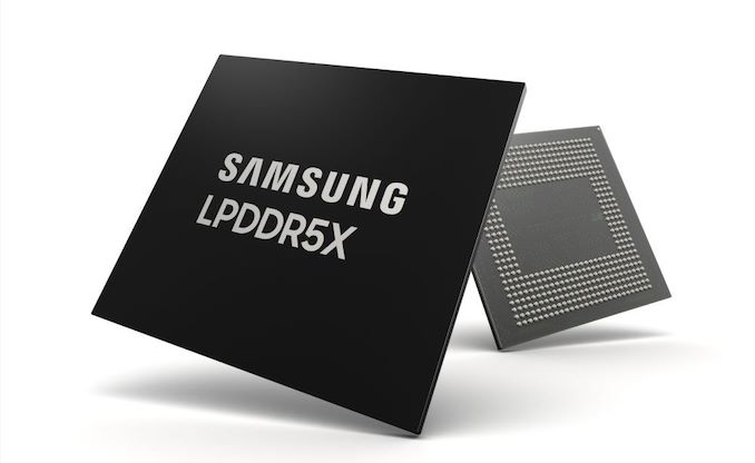
The verification process involved Samsung's 16 GB LPDDR5X package and MediaTek's soon-to-be-announced Dimensity 9400 SoC for high-end 5G smartphones. Usage of LPDDR5X-10700 provides a memory bandwidth of 85.6 GB/second over a 64-bit interface, which will be available for bandwidth-hungry applications like graphics and generative AI.
"Working together with Samsung Electronics has made it possible for MediaTek's next-generation Dimensity chipset to become the world's first to be validated at LPDDR5X operating speeds up to 10.7Gbps, enabling upcoming devices to deliver AI functionality and mobile performance at a level we have never seen before," said JC Hsu, Corporate Senior Vice President at MediaTek. "This updated architecture will make it easier for developers and users to leverage more AI capabilities and take advantage of more features with less impact on battery life."
Samsung's LPDDR5X 10.7 GT/s memory in made on the company's 12nm-class DRAM process technology and is said to provide a more than 25% improvement in power efficiency over previous-generation LPDDR5X, in addition to extra performance. This will positively affect improved user experience, including enhanced on-device AI capabilities, such as faster voice-to-text conversion, and better quality graphics.
Overall, the two companies completed this process in just three months. Though it remains to be seen when smartphones based on the Dimensity 9400 application processor and LPDDR5X memory are set to be available on the market, as MediaTek has not yet even formally announced the SoC itself.
"Through our strategic cooperation with MediaTek, Samsung has verified the industry's fastest LPDDR5X DRAM that is poised to lead the AI smartphone market," said YongCheol Bae, Executive Vice President of Memory Product Planning at Samsung Electronics. "Samsung will continue to innovate through active collaboration with customers and provide optimum solutions for the on-device AI era."
More...


 Quote
QuoteThread Information
Users Browsing this Thread
There are currently 41 users browsing this thread. (0 members and 41 guests)


Bookmarks