

Results 1,311 to 1,320 of 12096
Thread: Anandtech News
-
12-19-11, 04:10 PM #1311
Anandtech: AT&T Will Not Buy T-Mobile
AT&T has dropped its plans for a proposed $39 billion buyout of T-Mobile, citing interference from the FCC and the U.S. Department of Justice, the latter of which filed to block the merger back in August. AT&T will pay Deutsche Telekom, T-Mobile's parent company, $4 billion in recompense, and will enter into a "mutually beneficial roaming agreement" with the company at an unspecified future date.
AT&T will continue to invest in its network through a series of smaller deals, and calls on the FCC to approve its standing request to purchase unused Qualcomm spectrum - Verizon has taken similar steps to buy wireless spectrum from other companies in a series of smaller transactions, rather than buying out its competitors outright. AT&T also claims that regulatory interference is hindering its ability to meet its customers' needs, and calls on legislators to both "enact legislation to meet our nation's longer-term spectrum needs" and get out of the way so that "companies are allowed to react quickly to customer needs and market forces."
While AT&T says that the buyout's dissolution is bad for consumers, the government sees things differently - when the DoJ filed to block the AT&T merger, it said that T-Mobile represented an important competitive force in the cellular market, and its purchase would make it next to impossible for Sprint, the U.S.'s third-largest carrier, to compete with Verizon and AT&T.
Source: AT&T
More...
-
12-19-11, 07:30 PM #1312
Anandtech: Investigating the Galaxy Nexus LTE Signal Issue
It seems that each time an LTE handset comes out, there’s invariably some perceived issue with connectivity and stability. This time, focus is being placed on Verizon’s CDMA/LTE variant of the Galaxy Nexus, and the issue surrounds LTE connectivity robustness compared to the other LTE handsets out there.
I’ve been running battery life tests on our LTE Galaxy Nexus review unit since release day (a process that takes a considerable amount of time and results in our reviews posting a while behind everyone else’s), but have had some time to run tests and gauge subjective performance. I found that LTE connectivity and performance felt above average, subjectively, and noted that in a tweet. After complaints started to surface, I spent a considerable amount of time reading the threads on XDA and other places around the web trying to discern what the complaints are about. I’ve seen a couple of big misconceptions that I think really get to the heart of the matter.
First off, is some background. The Verizon CDMA/LTE Galaxy Nexus (codename “mysid”) uses a combination of Samsung CMC221 and Via Telecom CBP 7.1 for LTE and CDMA 1x/EVDO connectivity, respectively. This is virtually identical (unsurprisingly) to the Droid Charge, which used a CMC220 for LTE and the same CBP 7.1. The CMC22x family is UE Category 3, which currently is the highest for shipping devices and means it can handle up to 100 Mbps downstream with 20 MHz FDD. To date, all of the LTE basebands in Verizon LTE devices have been UE category 3 with the exception of Motorola’s devices, which are all UE category 2, but I digress. We’ve reached out to Samsung Semiconductor about what’s changed between CMC220 and 221, but doubtless the changes improve connection stability and reliability.
Speeds thus far have also been excellent. I’ve squeezed in 183 speedtests between battery life testing, and have seen some of the fastest LTE connectivity out of the Galaxy Nexus to date. After testing so many Motorola LTE devices with UE Category 2 modems, it’s refreshing to see this kind of performance out of a UE Category 3 device.
The issue that most people talk about centers around signal strength, and this is where a few misconceptions kick in. I’ve gotten a few emails and tweets and read pages on forums where people are implicitly comparing CDMA2000 1x/EVDO field strength to LTE field strength. The issue here is that on basically all of the LTE/CDMA Verizon handsets, the field under “Signal Strength” in about refers to EVDO signal strength, and not LTE signal strength. The two aren’t comparable at all for a host of reasons - different spectrum (800 MHz and 1900 MHz for 1x/EVDO as opposed to 700 MHz for LTE), and different cells (there’s some correlation, but not every Verizon base station has LTE onboard). The end result is that if you’re comparing 1x/EVDO signal strength to LTE signal strength, you’re making an absolutely meaningless apples to oranges comparison.


The Galaxy Nexus (and really just Android 4.0) now correctly reports and accommodates LTE by reporting its signal strength under “About->Status” and visualizing that as bars appropriately. Switch to EVDO on the Galaxy Nexus and signal strength appropriately changes to reflect an entirely different air interface’s signal strength. It’s nice to see people using dBm instead of bars when possible (which are effectively meaningless as a comparison metric), but now that there are multiple air interfaces on handsets, we have to be explicit about what numbers we’re actually comparing.
This is not a valid comparison - LTE versus EVDO signal strength
This reporting is a problem I’ve talked about at length in more than one LTE handset review, and to date I only know of ways to show LTE signal strength and channel quality on a few handsets. Samsung’s Droid Charge (courtesy Samsung’s excellent ServiceMode application viewed through *#0011# after some unlock trickery) and the Bionic (through logcat and grepping for the radio signal status daemon) report LTE field strength, but only if you dig for them.
Comparing LTE Signal Strength the Right Way
So how does the LTE Galaxy Nexus compare to the Droid Charge and Bionic, the two handsets we can actually view LTE signal strength in dBm on? Very closely as a matter of fact.
I have a Bionic kicking around which has to go back very soon, but fired up logcat and put the Galaxy Nexus next to it. The Bionic reports signal strength pretty constantly whereas in Android 4.0 the number has some hysteresis, but here the numbers are pretty darn close, with the Bionic hovering between -91 and -95 dBm, and the Galaxy Nexus reporting an average of -92 dBm.
Since the Droid Charge is the only other handset I know how to show LTE signal strength on, I tracked a friend down at a local cafe with one and fired up service mode. Again, what’s shown under “About->Status” on the Droid Charge is actually EVDO signal strength. Here the Galaxy Nexus shows -107 dBm and the Droid Charge shows -108 dBm.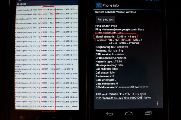
Left: Motorola Droid Bionic (logcat showing LTE signal strength), Right: Galaxy Nexus
The Droid Charge is another hilarious example of why you can’t compare bars at all, as the Charge shows a positively laughable 4 out of 5 bars in an area with very low LTE signal strength, whereas the Galaxy Nexus (moreover, Android 4.0) has a very conservative and realistic strength to bars mapping. Carriers love to make things out to be better than they really are, however, and the result is this kind of hilarious visualization which portrays LTE signal as being much better than it really is if you stare at bars all day.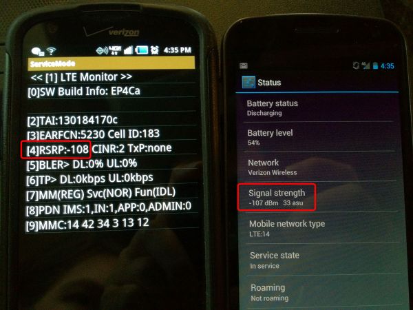
Left: Samsung Droid Charge (ServiceMode) Right: Galaxy Nexus
Verizon confirming though a tweet that there’s some sort of signal issue affecting the Galaxy Nexus confuses me, since from my perspective there isn’t any issue at all. The only real issue that exists is that the Galaxy Nexus (and really just the stock Android 4.0 signal strength to bars mapping) doesn’t line up with what Verizon has shipped on other devices, thus leading people to make apples to oranges comparisons and imagine an issue. I wager that some of this confusion is also compouned from the number of Verizon customers that are just now getting their first LTE handset with the Galaxy Nexus. It might be surprising to discover that LTE coverage right now isn't nearly as good as 1x/EVDO, but these things will improve as the carrier's LTE rollout continues. The other big disclamer is that I haven't fully investigated 1x/EVDO performance on the Galaxy Nexus, but this will end up being virtually idental to the Droid Charge.
There’s a CDMA and LTE baseband update coming with the LTE Galaxy Nexus’ 4.0.3 update as shown above, but this will likely do more to address connection stability than change the way anything is reported. Given how much attention this has gotten, however, I would not be surprised to see Google make a change to its signal strength to bars mapping for LTE and placebo away an issue that never really existed to begin with. That's also an unfortunate change, since from my perspective the Galaxy Nexus is one of the first handets that doesn't have an unrealistic mapping. In the meantime, we're still working on our Galaxy Nexus review where we'll take a complete look at the LTE/CDMA and GSM/UMTS Galaxy Nexii.
More...
-
12-20-11, 07:00 AM #1313
Anandtech: Samsung Promises Ice Cream Sandwich By 1Q12 For SGSII & Galaxy Note
In a post on Samsung Tomorrow, Samsung Electronics announced that they would begin rolling out Ice Cream Sandwich to the Galaxy S II variants and Galaxy Note by the end of the first quarter in 2012. This matches up fairly well with the timelines laid out by other manufacturers and they should hopefully meet their targets. Additional devices would be updated soon after and include the Galaxy R, Galaxy Tab 10.1, Galaxy Tab 8.9, Galaxy Tab 7.7 and Galaxy Tab 7.0 Plus. Stateside, carrier testing will play a role in when we see the updates.
Samsung developers have spent the most time with the Ice Cream Sandwich code, having collaborated with Google for the Galaxy Nexus. They will also be possibly the only manufacturer to develop Ice Cream Sandwich ports on the four current platforms. The Galaxy Nexus exposed them to TI OMAP 4, their Galaxy R and most of their Galaxy Tab line-up brings Tegra 2, most SGSII variants use Exynos with the exceptions being the LTE and T-Mobile variants, which use Qualcomm Snapdragon S3. So many platforms could lead to delays in updating certain devices, though their lead time should help mitigate this.
What won't help in a timely updateis the inclusion of TouchWiz. A leaked alpha ROM circulated last week with Samsung's skin layered atop Android 4.0. While we've praised Samsung's developer wizardry for improving UI speed and browser rendering, the styling and widgets of TouchWiz are a bit more of an acquired taste.
Lastly, the Galaxy Note recently made an appearance at the FCC, sporting AT&T friendly frequencies, so we might see the 5.3" phone/tablet at CES next month. There's also been some speculation that an LTE version of the Note would appear on AT&T. If the rumor is to be believed, it would likely sport the same Qualcomm-based configuration as the Galaxy S II LTE (AT&T's Skyrocket in the US).
More...
-
12-20-11, 10:30 AM #1314
Anandtech: AMD Intros New Unlocked K-Series Llano APUs: A8-3870K & A8-3670K
When we first reviewed Llano we thought it was a fairly competent desktop part if you needed a solution that didn't rely on discrete graphics. My biggest issue with Llano on the desktop was its price, at $135 for the top end A8 it seemed a bit too high. Today AMD is using the normal process improvements you see with any design over time to deliver a slight frequency bump without increasing prices. The extra 100MHz you get at the $135 and $115 price points isn't really going to change much, however AMD is introducing two K-series parts (they are also known as Black Edition SKUs) into the Llano lineup:
The A8-3870K and 3670K are partially unlocked parts allowing you to overclock an extra 500MHz on the CPU clock and an extra 200MHz on the GPU clock. Stock Llano parts are multiplier locked above their default multiplier and their GPU frequency isn't adjustable from what we've seen. AMD's new K-series SKUs give you another 5 multipliers above the default multiplier on the CPU side, and let you ramp up the GPU clock independently as well. In our original overclocking experiments we found that hitting 3.5 - 3.7GHz via bus overclocking on an A8-3850 wasn't too difficult, so these new K-series parts should let you reach close to what you could before without as much effort. In theory it should be pretty effortless to take a 3670K and turn it into something a bit faster than a 3870K, allowing you to pocket the $20 difference.AMD's Updated Llano Desktop Lineup GPU Total TDP (GPU + CPU) CPU Cores CPU Clock (Base/Turbo) GPU Cores GPU Clock Price AMD A8-3870K Radeon HD 6550D 100W 4 3.0GHz (unlocked) 400 600MHz (unlocked) $135 AMD A8-3850 Radeon HD 6550D 100W 4 2.9GHz 400 600MHz $135 AMD A8-3820 Radeon HD 6550 65W 4 2.5/2.8GHz 400 600MHz $??? AMD A8-3800 Radeon HD 6550D 65W 4 2.4/2.7GHz 400 600MHz $129 AMD A8-3670K Radeon HD 6530D 100W 4 2.7GHz (unlocked) 320 444MHz (unlocked) $115 AMD A6-3650 Radeon HD 6530D 100W 4 2.6GHz 320 444MHz $115 AMD A6-3620 Radeon HD 6530D 65W 4 2.2/2.5GHz 320 444MHz $??? AMD A6-3600 Radeon HD 6530D 65W 4 2.1/2.4GHz 320 444MHz $109 AMD A6-3500 Radeon HD 6530D 65W 3 2.1/2.4GHz 320 444MHz $85 AMD A4-3420 Radeon HD 6410 65W 2 2.8GHz 160 600MHz $?? AMD A4-3400 Radeon HD 6410 65W 2 2.7GHz 160 600MHz $71 AMD A4-3300 Radeon HD 6410 65W 2 2.5GHz 160 444MHz $66
The 3x20 parts are new as well - these are mild speed bumps over their 3x00 predecessors. These parts are available starting today:
There are also new mobile Llano parts being officially announced today, although we already reported on them earlier.
AMD Llano Mobile CPU refresh Name Cores CPU Clock
(Max Turbo)L2 Cache GPU GPU Cores GPU Clock TDP A8-3550MX 4 2.0GHz (2.7GHz) 4MB HD 6620G 400 444MHz 45W A8-3520M 4 1.6GHz (2.5GHz) 4MB HD 6620G 400 444MHz 35W A6-3430MX 4 1.7GHz (2.4GHz) 4MB HD 6520G 320 400MHz 45W A6-3420M 4 1.5GHz (2.4GHz) 4MB HD 6520G 320 400MHz 35W A4-3330MX 2 2.2GHz (2.6GHz) 2MB HD 6480G 240 444MHz 45W A4-3320M 2 2.0GHz (2.6GHz) 2MB HD 6480G 240 444MHz 35W A4-3305M 2 1.9GHz (2.5GHz) 1MB HD 6480G 160 593MHz 35W
More...
-
12-20-11, 11:40 PM #1315
Anandtech: Apple Acquires Anobit: Bringing NAND Endurance Technology In-House
I'd seen speculation that Apple was going to drop $500M on Anobit over the past few weeks. Ars Technica also published a piece believing the acquisition to be true, and it looks like the office of Israel's Prime Minister tweeted a bit of a confirmation (Anobit is based in Israel). I looked at Anobit's extremely vague technology descriptions and dug a bit into their patent portfolio to better understand Apple's motivation behind the acquisition.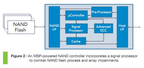
If you've followed our SSD coverage over the years you'll know that NAND endurance was a valid concern in the early days of consumer SSDs. When Intel arrived on the scene with the X25-M, its controller technology included a number of enhancements to work around common NAND errors and degradation over time. Other companies followed suit and eventually NAND error correction and reliability were major selling points of SSD controllers.
More recently, Micron announced that it would be baking ECC technology into a separate line of NAND called Clear NAND. Micron believes that in the future if you don't have access to a controller that does significant ECC or a NAND solution that includes active ECC technology that you won't be able to deliver competitive NAND based storage.
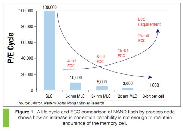
Today not much of this is necessary for consumer SSDs, even forthcoming 20nm IMFT NAND is still good for 3000 - 5000 program/erase cycles, which is more than enough for client use. However if you're using greater than 2-bit-per-cell MLC (e.g. 3-bit-per-cell MLC) then the need for better error correction is more urgent.
Smartphones and tablets need not-insignificant amounts of NAND (16 - 64GB for high end devices today, twice that next year). The cost of this NAND isn't all that much in the grand scheme of things, at the low end you're looking at several dollars and at the high end the cost is more than offset by the ridiculous increase in device pricing. The problem is not at the high end but what happens when you start selling cheaper phones. If we are indeed heading toward a future where mainstream computing is done on smartphones, then we're also headed toward a future where all smartphones need dozens of GBs of NAND on-board. That includes the ultra cheap devices as well as the high-end flagships.
Price sensitivity in these devices means that the high grade, compute NAND used in SSDs isn't what gets used by smartphone manufacturers. Instead you get the mid-grade stuff at best, but more likely you find some slow, 3-bit-per-cell NAND in the cheaper devices. There's no room (physically or budget) for sweet SSD controllers by Intel, Marvell or SandForce, thus NAND management is typically handled by an eMMC controller (or something similar) integrated into the phone/tablet's applications processor (e.g. Snapdragon, Tegra 3, A5, etc...).
Cheaper MLC NAND trades off endurance and performance for cost. How do you get to have your cake and eat it too? Well if you're set on using cheaper NAND, you have to do more processing on the controller side to clean up the data you're reading back from the shaky NAND. This isn't a problem on day one, but it becomes an issue over the months/years as you've written more data to the NAND. Cells have to be periodically refreshed, storing redundant data becomes necessary, the controller must recover/reconstruct lost data, etc... Every company has their approach to dealing with these problems. It was the first solutions to these problems that allowed consumer SSDs to use cheaper MLC NAND, and the solution to the smartphone/tablet issue is of a similar nature.
Anobit appears to be applying a lot of signal processing techniques in addition to ECC to address the issue of NAND reliability and data retention. In its patents there are mentions of periodically refreshing cells whose voltages may have drifted, exploiting some of the behaviors of adjacent cells and generally trying to deal with the things that happen to NAND once it's been worn considerably.
Through all of these efforts, Anobit is promising significant improvements in NAND longevity and reliability. At the high end Anobit promises 50,000 p/e cycles out of consumer grade MLC NAND, and in the smartphone/tablet space Anobit promises more useful lifespan out of 3-bit-per-cell MLC NAND.
As for why Apple would want Anobit, the potential reasons are huge. First the company was a cheap buy for Apple, although expensive if you look at the market as a whole (SandForce went for ~$370M). If all Apple gains from Anobit is bringing some smart NAND folks on staff the cost won't really break the bank. The obvious fit is to integrate Anobit's technology into Apple's ARM based SoCs. These SoCs already talk to NAND directly and integrating better error correction/reliability processing into the SoC just makes sense. For all we know, Apple already uses this technology in its SoCs and is simply acquiring Anobit to make it more difficult for competing SoC makers to do the same. Integration and assimilating value are the cornerstones of building a good SoC, this move makes sense (assuming Anobit's technology is actually good).
Note that if you look at the graph above, continuing to use 3-bit-per-cell NAND requires more than just standard ECC. It's clear Apple wants to continue to use value NAND in its devices, Anobit is simply a guarantee that it will be able to do so in the future.
At the other end of the spectrum, Anobit has enough technology to build a decent SSD controller (it already appears to do so for enterprise SSDs). If Apple wanted to really commoditize SSDs, it could use Anobit to produce its own SSD controllers. Apple would then simply buy NAND from memory vendors instead of the present day solution of buying a complete SSD solution for its Macs. This would shave a not insignificant portion of the BOM (bill of materials) cost of SSD production, which would help Apple transition to SSDs in more of its systems. This is more of a longshot as far as I'm concerned as, at least today, there are a lot of low-cost, competent controller makers in the SSD space.
Apple has been internalizing many of the pieces used in its SoCs over the past few years. It even owns a 9.5% stake in Imagination Technologies, the GPU company that supplies IP for Apple's SoCs. While I understand Apple's motives from the standpoint of a mostly vertically integrated hardware/software entity, there is a bit of defocus that comes with going too far down this path. I'm still not sold on the idea of Apple becoming a full fledged silicon vendor. It makes sense today, but as these SoCs become hugely complex, billion+ transistor devices I'm unsure if Apple wants to assume even more of the burden involved in bringing one of those parts to market.
Until we get to that point however, acquistions like Anobit come relatively cheaply for Apple and should help guarantee NAND reliability and performance for its more cost sensitive products (particularly as NAND geometries continue to shrink going forward). If Anobit's technology is up to muster, it should also mean that Apple will be able to continue to scale up NAND capacities in its devices without resorting to increasing device costs. NAND is ultimately driven by Moore's Law, however reliability doesn't follow the same curve by default. Integration of Anobit-like technologies are necessary to ensure it does.
More...
-
12-21-11, 04:50 AM #1316
Anandtech: Ultrabook Head to Head: Acer Aspire S3 vs. ASUS UX31E
Intel first launched the ultrabook concept back in May of this year, and the initial reaction ranged from cynicism to excitement. On the one end of the spectrum were those who just saw the ultrabook as a way for Intel to try and sell more high-margin ULV parts, along with others calling the whole thing a MacBook Air knockoff. Those who showed more enthusiasm for the platform had a different take on things: who cares if it’s just a rebranding or a knockoff? If it’s a way to get less expensive laptops with a great aesthetic and SSDs for everyone, sign me up! Naturally, there are plenty of others who fall more in the middle. For this group, it doesn’t matter what marketing might say; “show us what you’ve got” is their motto, and if you build a good product at an appropriate price, they’ll be happy to recommend and/or buy it.
Today, we have two more ultraportables to put under the microscope. The first is the big brother to the UX21E that we already reviewed, the ASUS UX31E. The second comes from Acer and targets a lower price point by trimming a few extras. We’ll also have some discussion of the broader ultrabook market and who might benefit from a look at the various offerings. If you’re thinking an ultrabook (or an ultraportable) might be the right choice for your next laptop, or if you just want to see what they have to offer, read on.
More...
-
12-21-11, 09:10 AM #1317
Anandtech: Firefox 9 Released, Brings JavaScript Speed Improvements
Mozilla is in the process of pushing Firefox 9 out to users on its release channel, about six weeks after the release of Firefox 8. The major stated improvement to Firefox 9 is what Mozilla calls the Type Interface for JavaScript, which it says improves performance up to 30 percent in some benchmarks. To test this, I ran a few quick SunSpider tests to compare performance to older versions of Firefox and current versions of Chrome and Safari. These tests were run on a 2010 iMac running OS X 10.7.2 with all updates installed and are only meant to measure relative performance between browsers running on the same computer.
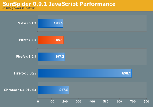 In a standard SunSpider run, Firefox 9 is consistently faster than Firefox 8, but not by anywhere near 30 percent (bearing in mind, of course, that this is just one synthetic benchmark among many). Also note that JavaScript numbers are just one facet of performance - while Safari edges out Firefox 9, to me it seemed a bit slower than both Firefox and Chrome when launching and loading pages. All current browsers completely wipe the floor with Firefox 3.6, both in JavaScript numbers and in apparent speed, so whatever you use you're going to be browsing much faster than you could at the beginning of the year. Increased competition has clearly been good for the browser market.Firefox 9 also brings two-finger navigation to users running OS X Lion - swiping left on a multitouch device will go back, and swiping right will go forward. Safari and Chrome have already implemented this feature, and while the functionality is the same in Firefox, those browsers include visual cues (arrows in Chrome, a visual sliding of the page in Safari) to let you know that you're doing it, visual feedback that I find helpful. There's still no support for fullscreen mode, though plugins exist to give this functionality to those who want it.
The rest of the improvements can be found in the usual laundry list of small security and bug fixes (including one I had run into where attachments wouldn't download properly when using the Outlook Web App - useful information for shops running an Exchange server). You can get the new browser by using Firefox's built-in updater or by visiting getfirefox.com.
Note: At the moment, Mozilla says that it's not pushing Firefox 9 out to OS X and Linux users automatically because of "a possible issue affecting a small number of users." We'll keep an eye on this and update the post as events progress.
Source: Mozilla
More...
-
12-21-11, 03:20 PM #1318
Anandtech: Intel Shows Off Competitive Medfield x86 Android Power & Performance
You may have seen some Medfield related news today - I thought I'd chime in with some of my thoughts on the topic. As a recap, in 2008 Intel introduced its Atom microprocessor - originally designed for MIDs (Mobile Internet Devices) and repurposed for use in netbooks. In 2010 we got a more integrated version of Atom called Moorestown designed for smartphones and tablets. Intel had basically no success with Moorestown, although Pineview (its netbook counterpart) was still used in netbooks. In our original architecture piece I called Moorestown the "two-chip solution that uses five chips". Despite physical real estate requirements, Moorestown could fit into something that was a bit larger than an iPhone at the time. At the time everyone assumed Moorestown didn't make it into a phone because of unreasonably high power draw, but no one was able to back up those claims with actual test data. Intel will tell you that Moorestown never made it anywhere because it lacked platform focus. Intel was off chasing Moblin/MeeGo and Android wasn't a priority. Things have obviously changed since then.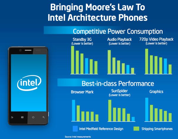
Medfield is the 32nm successor to Moorestown. Intel hasn't disclosed many details about Medfield's architecture, but we do know that it is a more integrated single chip design (compared to Moorestown's "two-chip" solution). We also saw Intel's Medfield reference smartphone and tablet, both running Android, at IDF. While this is still far away from announcing an actual design win, it's clear that Intel is finally making progress in the right direction. Couple these recent milestones with more recent restructuring inside Intel and it looks like the company is finally preparing to really enter the mobile market.
This brings us back to today's news. The information disclosed today came from an investor conference earlier this month. Above is a slide from the aforementioned meeting.
Intel has carefully removed the names of the devices in this chart. Barring any outright deception however, there seems to be potential in Medfield. One would assume that device manufacturers are given access to this (and more) performance data. One might also be able to infer that if Intel does indeed have a Medfield design win (hopefully more than one), then these numbers might be fairly convincing. The war begins in 2012...
Gallery: Intel's Medfield Gingerbread Smartphone Reference Platform


More...
-
12-21-11, 11:10 PM #1319
Anandtech: AMD Radeon HD 7970 Review: 28nm And Graphics Core Next, Together As One
While AMD and NVIDIA are consistently revising their GPU architectures, for the most part the changes they make are just that: revisions. It’s only once in a great while that a GPU architecture is thrown out entirely, which makes the arrival of a new architecture a monumental occasion in the GPU industry. The last time we saw this happen was in 2006/2007, when unified shaders and DirectX 10 lead to AMD and NVIDIA developing brand new architectures for their GPUs. Since then there have been some important revisions such as AMD’s VLIW4 architecture and NVIDIA’s Fermi architecture, but so far nothing has quite compared to 2006/2007, until now.
At AMD’s Fusion Developer Summit 2011 AMD announced Graphics Core Next, their next-generation GPU architecture. GCN would be AMD’s Fermi moment, where AMD got serious about GPU computing and finally built an architecture that would serve as both a graphics workhorse and a computing workhorse. With the ever increasing costs of high-end GPU development it’s not enough to merely develop graphics GPUs, GPU developers must expand into GPU computing in order to capture the market share they need to live well into the future.
At the same time, by canceling their 32nm process TSMC has directed a lot of hype about future GPU development onto the 28nm process, where the next generation of GPUs would be developed. In an industry accustomed to rapid change and even more rapid improvement never before have GPU developers and their buyers had to wait a full 2 years for a new fabrication process to come online.
All of this has lead to a perfect storm of anticipation for what has become the Radeon HD 7970: not only is it the first video card based on a 28nm GPU, but it’s the first member of the Southern Islands and by extension he first video card to implement GCN. As a result the Radeon HD 7970 has a tough job to fill, as a gaming card it not only needs to deliver the next-generation performance gamers expect, but as the first GCN part it needs to prove that AMD’s GCN architecture is going to make them a competitor in the GPU computing space. Can the 7970 do all of these things and live up to the anticipation? Let’s find out…
More...
-
12-22-11, 02:50 AM #1320
Anandtech: Sandy Bridge E & X79 PCIe 3.0: It Works
At the launch of Intel's LGA-2011 based Sandy Bridge E CPU we finally had a platform capable of supporting PCI Express 3.0, but we lacked GPUs to test it with. That all changed this past week as we worked on our review of the Radeon HD 7970, the world's first 28nm GPU with support for PCIe 3.0.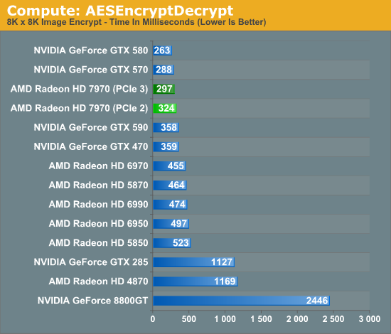
The move to PCIe 3.0 increases per-lane bandwidth from 500MB/s to 1GB/s. For a x16 slot that means doubling bandwidth from 8GB/s under PCIe 2.1 to 16GB/s with PCIe 3.0. As we've seen in earlier reviews and our own internal tests, there's hardly any difference between PCIe 2.1 x8 and x16 for modern day GPUs. The extra bandwidth of PCIe 3.0 wasn't expected to make any tangible difference in gaming performance and in our 7970 tests, it didn't.
Why implement PCIe 3.0 at all then? For GPU compute. Improving bandwidth and latency between the CPU and the GPU are both key to building a high performance heterogenous computing solution. While good GPU compute benchmarks on the desktop are still hard to come by, we did find one that showed a real improvement from PCIe 3.0 support on the 7970: AMD's AES Encrypt/Decrypt sample application.
Simply enabling PCIe 3.0 on our EVGA X79 SLI motherboard (EVGA provided us with a BIOS that allowed us to toggle PCIe 3.0 mode on/off) resulted in a 9% increase in performance on the Radeon HD 7970. This tells us two things: 1) You can indeed get PCIe 3.0 working on SNB-E/X79, at least with a Radeon HD 7970, and 2) PCIe 3.0 will likely be useful for GPU compute applications, although not so much for gaming anytime soon.
More...


 Quote
QuoteThread Information
Users Browsing this Thread
There are currently 34 users browsing this thread. (0 members and 34 guests)


Bookmarks