

Results 2,371 to 2,380 of 12091
Thread: Anandtech News
-
11-13-12, 09:30 AM #2371
Anandtech: AnandTech/Intel SSD Webcast Live Today at 9AM PST/12PM EST
We are live at SC12 from Salt Lake City, Utah this morning and are preparing to answer your SSD, NAND and Intel SSD DC S3700 questions. In about two hours I'll be on a replica bridge set of the starship Enterprise from the original series, alongside Intel's Roger Peene, answering your questions live. Although its a replica of the original bridge, it is an officially sanctioned reproduction by Paramount.
We'll be talking about the S3700, SSDs in general, NAND architecture and even the future of solid state storage. It should be an awesome discussion.
If you didn't get to comment in the previous post prior to today you will be able to submit questions live during the webcast. Here's the link to the webcast which will begin at 9AM PST/12PM EST today. 


More...
-
11-13-12, 10:30 AM #2372
Anandtech: The Droid DNA Announced: 5-inch, 1080p, S4 Pro
%5B4%5D_575px.jpg) You've seen the leaks, but now it's real. HTC and Verizon have just announced the Droid DNA, a 5-inch behemoth sporting an incredible 1080p Super LCD3 display. Powering those pixels is the capable Snapdragon S4 Pro SoC, familiar to us as the APQ8064 with 4 Krait cores running at 1.5GHz and last seen in the Nexus 4. For modem, the Droid DNA is using MDM9615 which makes this HTC's first Qualcomm Fusion 3 based device. The Droid DNA also includes ImageChip and the usual ImageSense features, and brings the 2.1 MP F/2.0 camera we saw on the HTC 8X as well. There's 2 GB of RAM onboard as well.
You've seen the leaks, but now it's real. HTC and Verizon have just announced the Droid DNA, a 5-inch behemoth sporting an incredible 1080p Super LCD3 display. Powering those pixels is the capable Snapdragon S4 Pro SoC, familiar to us as the APQ8064 with 4 Krait cores running at 1.5GHz and last seen in the Nexus 4. For modem, the Droid DNA is using MDM9615 which makes this HTC's first Qualcomm Fusion 3 based device. The Droid DNA also includes ImageChip and the usual ImageSense features, and brings the 2.1 MP F/2.0 camera we saw on the HTC 8X as well. There's 2 GB of RAM onboard as well.
The style of the phone alludes to its Incredible forebears, but only in the bright red accents. The design is sleeker, with a smooth back and thin profile. On the long edges of the phone are large red grills, though stereo speakers are not in order. What is available to audiophiles, is a 2.55v built-in headphone amp, not a common find in a smartphone but something that will go a long way to improving the listening experience. 

More...
-
11-13-12, 06:00 PM #2373
Anandtech: HTC Droid DNA Hands-On
Today’s HTC Droid DNA announcement brings a few big advancements over the HTC One X that never made it to Verizon's line-up. We'll start our hands-on discussion with the most obvious change: the screen.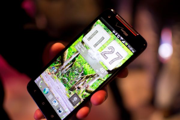
The Display
 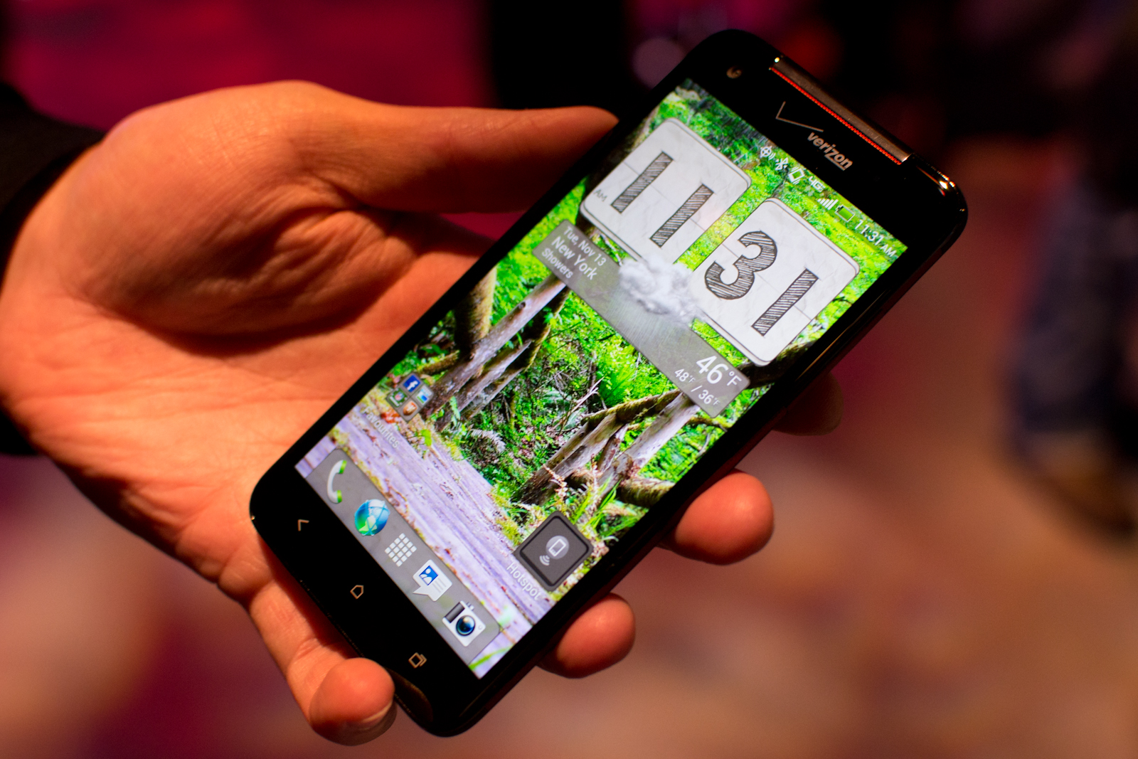
The rapid advance of screen technology means that we're just a year removed from the arrival of 720p displays, and just two years removed from WVGA being the defacto resolution. Today we see the efforts of Sharp’s display team come to fruition with a seemingly uncompromised 5" 1080p display. The pixel density is an unchallenged 440 ppi, and it seems to retain the brightness and fidelity of its predecessors, most recently seen in the HTC One X. 
Hands-on events aren’t the place for detailed analysis, the time is too short, and the venues to cramped to pull out a colorimeter. What I will say is that the display is easy on the eyes and offers such a glut of pixels that no amount of squinting allowed me to discern. Viewing angles seemed good, with no distortion noted, and colors were bright without being oversaturated. So, at first glance, a somewhat expected excellent for the display. Here’s the thing: do we want a 1080p 5” display? At this pixel density, we would be approaching an angular subtense of two thirds of a degree. That's well below the human ability to discern at twelve inches. So is the likely battery hit worth the improved pixel density? We'll have to wait and see. 
 
The Design
The great display is surrounded by narrow bezels all around, and the result is a body that is just 15 mm longer than the One X, despite the larger screen, and less than a millimeter wider. Gorilla Glass 2 is used and actually extends across the entire face of the device and forms part of the edge of the handset, a surefire sign of confidence in the strength of the glass. The effect is to make the frong glass and back seem fused into one solid piece. Accent grills adorn the sides of the device, in the bright red we’ve come to expect from HTC phones on VZW. The back is a softly curving single expanse of matte black, with the HTC logo etched and inlayed in silver. An LTE logo, Beats Audio logo and the single speaker grill grace the bottom of the back, and the 8MP rear-shooter sits at the top. One particularly unique feature on the back is a concealed status LED to the left of the camera lens. When the phone is face down and a notification is received, the LED will blink to alert the user. The LED is also used to alert self-shooters when the shutter will release. 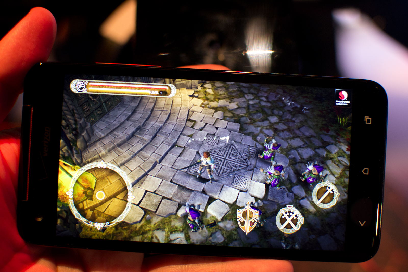
At nearly a centimeter at its thickest point, this is not the thinnest phone; but the way the back tapers down to the edge gives it an excellent in the hand feel, and makes it feel thinner than its specifications would indicate. Despite deviations from the One series design language, the solidity that defines that lineage can be seen here. 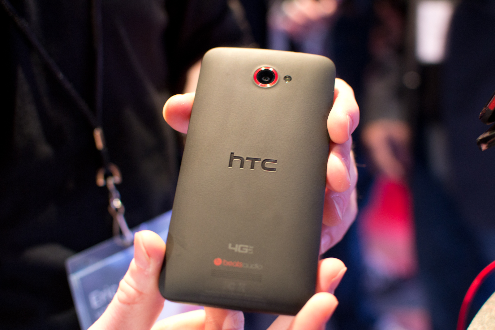
 
 Physical Comparison   HTC Droid DNA HTC One X (AT&T) Samsung Galaxy S 3 (USA) LG Nexus 4 Height 141 mm (5.55") 134.8 mm (5.31" ) 136.6 mm (5.38") 133.9 mm (5.27") Width 70.5 mm (2.78") 69.9 mm (2.75") 70.6 mm (2.78") 68.7 mm (2.7") Depth 9.73 mm (0.38") 8.9 mm (0.35") 8.6 mm (0.34") 9.1 mm (0.36") Weight 142 g (5.01 oz) 129 g (4.6 oz) 133 g (4.7 oz) 139 g CPU 1.5 GHz APQ8064 (Quad Core Krait) 1.5 GHz MSM8960 (Dual Core Krait) 1.5 GHz MSM8960 (Dual Core Krait) 1.5 GHz APQ8064 (Quad Core Krait) GPU Adreno 320 Adreno 225 Adreno 225 Adreno 320 RAM 2 GB LPDDR2 1 GB LPDDR2 2 GB LPDDR2 2 GB LPDDR2 NAND 16 GB NAND 16 GB NAND 16/32 GB NAND with up to 64 GB microSDXC 8/16 GB NAND Camera 8 MP with AF/LED Flash, 2.1MP front facing 8 MP with AF/LED Flash, 1.3 MP front facing 8 MP with LED Flash + 1.9 MP front facing 8 MP with AF/LED Flash, 1.3 MP front facing Screen 5" 1920 x 1080 LCD-TFT 4.7" 1280x720 LCD-TFT 4.8" 1280x720 HD SAMOLED 4.7" 1280x768 HD IPS+ LCD Battery Internal 7.47 Whr Internal 6.66 Whr Removable 7.98 Whr Internal 8.0 Whr
The Camera
 
Cameras, like displays before them, were long ignored as just value adds, and not features that must be optimized and perfected. It’s really exciting to see manufacturer’s compete for the best phone camera and not just through software trickery. HTC’s approach is, perhaps, the most traditional, and that is to provide an optical package that mimics the higher-end discrete glass you’d find on a proper SLR. The same f/2.0 28mm optics package is used here, as in the One X, and most likely the same sensor is in play. The ImageChip ISP remains a feature, and the software (now called Sense 4+) has a few additions to improve usability. It’ll be interesting to see how Sense 4+ and Android 4.2’s new camera software will play together, but for now the camera seems intuitive and the results look to match that of the One X. 


The front-camera from the HTC WIndows Phone 8X finds a home here, bringing its f/2.0 optics, ultra-wide angles and 2.1MP sensor, which shoots 1080p video.
 
The SoC
 
Obviously, we’ve spent a little time with this particularly SoC, recently. UI performance was smooth, and hard to trip up, even with the graphical flourishes HTC favors. The home screen carousel is no more, but cycling through home screens remains a wrap around affair and a second tap on the home button still brings an overview of all your home screens. All those flourishes render fluidly, and hopping in an out of apps and the app drawer, I didn't notice any particular hiccups. Performance should be excellent in our typical tests, based on SoC alone, but software is always a key component to the experience, and it'll be interesting to see how this S4 Pro equipped handset differs from the Nexus 4 and LG Optimus G. 
 
The Audio
 
HTC has been focusing on handset audio for sometime, including their investment in and use of Beats Audio's DSP algorithms. Beats Audio remains, and there’s even a VZW tie-in with the Beats Pill, a portable Bluetooth speaker. Added to the mix is a dedicated 2.55v headphone amp, which should be able to drive even the most high-end cans. Sound quality should be improved in all headphones, and they were certainly able to power my modest earbuds well. No specifics were provided, but a dedicated amp for the rear speaker should give audio a boost there, as well. This sort of focus on audio quality is always nice to see, and we’ll be excited to put the DNA through its paces to see how it stacks up. 
Gallery: How To Build A 5-inch Phone: HTC Droid DNA Hands-On


More...
-
11-14-12, 01:00 PM #2374
Anandtech: The Xeon Phi at work at TACC
The Xeon Phi family of co-processors was announced in June, but Intel finally disclosed additional details about the first shipping implementation of Larrabee. In this short article we'll go over the different Xeon Phi SKUs, what kind of software runs on it and how the Xeon Phi are implemented in a supercomputer.
We had the chance to briefly visit Stampede, the first Supercomputer based upon the Xeon Phi in Austin, TX. Stampede is the most powerful of the supercomputers at the Texas Advanced Computing Center (TACC).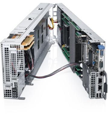
 
 
More...
-
11-14-12, 01:00 PM #2375
Anandtech: Green500 Supercomputer List Released: Intel Takes Top Spot, Followed By AM
Coinciding with the publication of the Top500 supercomputer list earlier this week, the Top500’s sister list, the Green500, was published earlier this morning. The Green500 is essentially to power efficiency what the Top500 is to total performance, being composed of the same computers as the Top500 list sorted by efficiency in MFLOPS per Watt. Often, but not always, the most powerful supercomputers are among the most power efficiency, which can at times lead to surprises.
Much like the spring Top500 list, the spring Green500 list was dominated by IBM BlueGene/Q systems. With the assembly of a number of new heterogeneous supercomputers since then however, not only has BlueGene/Q been dethroned from the Top500 list, but now the Green500 list as well. In its place on both lists are systems using co-processors from all of the big three: Intel, AMD, and NVIDIA.
For the latest Green500 list, the #1 spot on the latest Green500 list goes Beacon, a Xeon Phi based supercomputer running at the National Institute for Computational Sciences. At only 44.89 KW, Beacon is a much smaller installation than the likes of the major BlueGene/Q supercomputers or Titan (placing just #253 on the Top500), but Xeon Phi makes a very strong showing here as Intel’s first retail MIC co-processor. Altogether Beacon hit 2499.44 MFLOPS/W, nearly 400 MFLOPS/W higher than the BlueGene/Q computers it has surpassed.
Meanwhile at #2 on the Green500 is King Abdulaziz City for Science and Technology’s SANAM supercomputer, which is the only computer on the list powered by AMD GPUs. SANAM uses AMD’s recently announced FirePro S10000 cards, which are in turn composed of 2 of AMD’s Tahiti GPUs. While AMD has had a significant showing in the Green500 list for several years now from the CPU side of things, they have never been a contender as a co-processor vendor, so this is a significant breakthrough for AMD and their first modern GPU compute architecture, GCN. Though much like the Xeon Phi powered Beacon, SANAM is a relatively modest supercomputer; its 2351.1 MFLOPS/W efficiency being spread among only 179KW of total power consumption (making it #52 on the Top500).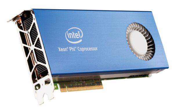
Finally, at #3 is Titan, the recently launched Tesla K20X based supercomputer at Oak Ridge National Laboratory. Titan is the current #1 computer on the Top500 list and larger than any other computer on the Green500 list, so along with their top showing on the Top500 list NVIDIA can now also claim to be powering one of the most efficient supercomputers in the world, a significant boost in prestige for their Tesla division. At 2142.77 MFLOPS/W for power efficiency Titan can’t quite match the top Intel and AMD systems, but it’s enough to push past BlueGene/Q just as it did on the Top500 list.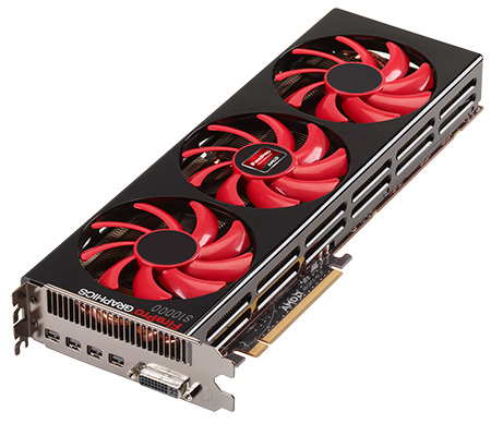
What’s interesting from all of this data is that of the top 10 computers on the Green500 list, the top four computers on the list are all heterogeneous systems using co-processors; the previous 3 systems being Intel, AMD, and NVIDIA, followed by NVIDIA again at #4. Just 6 months ago the CPU-only BlueGene/Q dominated the list, so for Intel, AMD, and NVIDIA to rocket to the top is a significant achievement for GPUs and GPU-like processors. The use of co-processors means that more traditional x86 CPUs are also along for the ride at the top of the list, with Intel and AMD each splitting the top of the Green500 list at 2 each. Ultimately this isn’t the first time heterogeneous systems have had a strong showing on the Green500, but this is the first time they’ve swept the top of the list like this, and marks a major leap in power efficiency for heterogeneous systems that finally puts them on-par with (and beyond) BlueGene/Q.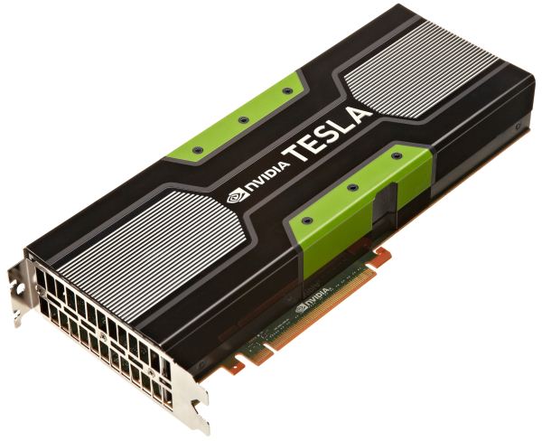

More...
-
11-14-12, 06:00 PM #2376
Anandtech: Android 4.2 Hits AOSP, Broadcom Replaces NXP with NCI Stack for NFC
Yesterday source code for Android 4.2 was pushed to AOSP (Android Open Source Project), paving the way for other developers to begin building their own Android images and looking through the source code changes made in Android 4.2 to the core of the Android OS. In conjunction with AOSP push, the Android 4.2 platform highlights page went live with more detail about new features in the point update from 4.1 to 4.2. We went over a number of the major user-facing features in our Nexus 4 and Android 4.2 review but there are a bunch of other noteworthy features outlined in the platform highlight details, including even more improvements made to the 2D rendering engine, WebView rendering engine (which doesn’t apply to Chrome unfortunately), and the new inclusion of GPU compute for Renderscript Compute which is an Android API for running code on CPU, GPU, and DSP. I’m sure we’ll be hearing even more about Renderscript Compute in the coming weeks. I’m burying the lead a bit here, because today Broadcom confirmed some observations I made about the Nexus 4 and Nexus 10 and their NFC solutions.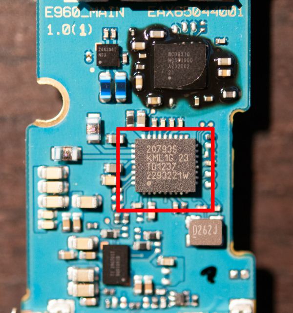
In the Nexus 4 review I noted that Broadcom’s BCM20793 appeared to have taken the slot of the up until now relatively ubiquitous NXP PN544 controller, which debuted with the Nexus S and has since been the go-to NXP controller for OEMs. In addition to taking the hardware slot, in the platform highlights page there’s a note about Broadcom also fully open sourcing its NFC NCI (NFC Controller Interface) stack which is a new NFC Forum specification designed to standardize the abstraction layer between NFC controller and SoC. Back when the Nexus S launched Google licensed and open sourced the NXP software stack for their NFC controllers, which has been inside Android ever since. I’m told that the NXP stack was previously tailor made to their hardware, and that with an NCI compliant stack OEMs will have greater flexibility when choosing an NFC controller. It makes sense that Google would want a stack with as much flexibility as possible and this gets changed up with 4.2.
I learned some details about BCM20793 as well. Broadcom’s NFC controller is built on a 40nm process and is compatible with both SIM and embedded secure elements (the Nexus 4 uses an embedded SE). In addition Broadcom believes its low power detection mode offers significantly lower idle power consumption than other solutions. Rather than inducing a field and polling for a tag or nearby device on a slotted cycle while the device is on, Broadcom’s “low power target detection” detects the change in antenna load caused by another NFC antenna being brought in proximity, and then polls. I’m told that this results in their controller inducing a field and burning current orders of magnitude less than other readers, and thus giving a fairly large power savings, in addition to the process advantage from 40nm. The obvious next step for Broadcom is to integrate this IP into a Wi-Fi, Bluetooth, FM combo like BCM4334, I wouldn’t be surprised to see something happen like that in the near future.
When I saw the BCM20793 in close proximity to the TI BQ51051b Qi wireless power receiver inside the Nexus 4, I suspected that part of the NXP shakeup might also involve some coexistence communication between the two. While there was RF planning involved (thankfully Qi works at a lower frequency than NFC), the NXP and Qi charging solutions still use different inductive loops and don’t need any collaborative communication. We haven’t talked a lot about the Nexus 10 or formally reviewed it yet, but interestingly enough has multiple NFC points of interest and is able to communicate through the front in addition to the back, and also appears to be BCM2079x based.
Source: Android Building, Android Platform Highlights, BCM2079x Family

More...
-
11-14-12, 11:30 PM #2377
Anandtech: Lenovo ThinkStation D30 Workstation Review: 16 Cores and 32 Threads Under
This month is a massive rush of new hardware. Users fond of high-powered portables are probably losing their minds; while Windows 8 and RT are of questionable value to desktop users, hardware designed to take advantage of them is flooding onto the market. Likewise, the SoCs powering smartphones continue to advance at a breakneck pace that hasn't really been seen since the dawn of the Pentium era. It's easy to forget that for how powerful portable technology has become, the potential for desktops and desktop workstations is downright monstrous.
For the foreseeable future, there will always be a need for CAD, video, and 3D rendering workstations. Basic desktop users see grossly diminishing returns on performance after about four logical cores (eight threads), but workstation tasks can still soak up every last ounce of performance you can throw at them. For major businesses where time very truly is money, that means needing the fastest hardware you can find and maintaining uptime for as long as humanly possible. That, in turn, means finding a workstation that's both reliable and easy to service. Lenovo hopes to address these needs with the ThinkStation D30, a dual-socket workstation capable of sporting up to sixteen cores and dual NVIDIA workstation cards (including the Quadro 6000 and Tesla cards for Maximus support)..jpg)

More...
-
11-16-12, 09:30 AM #2378
Anandtech: Samsung SSD 840: Testing the Endurance of TLC NAND
NAND endurance is something that always raises questions among those considering a move to solid state storage. Even though we have showed more than once that the endurance of today's MLC NAND based SSDs is more than enough for even enterprise workloads, the misconception of SSDs having a short lifespan still lives. Back in the day when we had 3Xnm MLC NAND with 5,000 P/E cycles, people were worried about wearing our their SSDs, although there was absolutely nothing to worry about. The move to ~20nm MLC NAND has reduced the available P/E cycles to 3,000, but that's still plenty.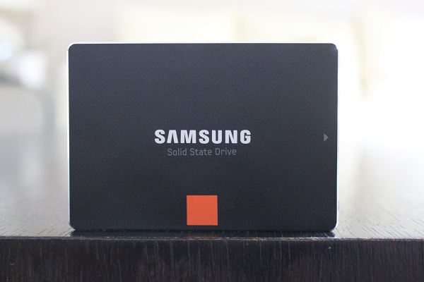
We have tested MLC NAND endurance before but with the release of Samsung SSD 840, we had something new to test: TLC NAND. We have explained the architectural differences between SLC, MLC and TLC NAND several times by now, but I'll do a brief recap here (I strongly recommend reading the detailed explanation if you want to truly understand how TLC NAND works):
The main difference is that MLC stores two bits per cell, whereas TLC stores three. This results in eight voltage states instead of four (also means that one TLC cell has eight possible data values). Voltages used to program the cell are usually between 15V and 18V, so there isn't exactly a lot room to play with when you need to fit twice as many voltage states within the same space. The problem is that when the cell gets cycled (i.e. programmed and erased), the room taken by one voltage state increases due to electron trapping and current leakage. TLC can't tolerate as much change in the voltage states as MLC can because there is less voltage headroom and you can't end up in a situation where two voltage states become one (the cell wouldn't give valid values because it doesn't know if it's programmed as "110" or "111" for example). Hence the endurance of TLC NAND is lower; it simply cannot be programmed and erased as many times as MLC NAND and thus you can't write as much to a TLC NAND based SSD.  SLC MLC TLC Bits per Cell 1 2 3 P/E Cycles (2Xnm) 100,000 3,000 1,000 Read Time 25us 50us ~75us Program Time 200-300us 600-900us ~900-1350us Erase Time 1.5-2ms 3ms ~4.5ms
No manufacturer has openly wanted to discuss the endurance of TLC, so the numbers we have seen before have been educated guesses. 1,000 - 1,500 P/E cycles is what I've heard for TLC NAND. The reality can also be different from what manufacturers claim as we discovered in the Intel SSD 335 (though there is a high probability that it's just a firmware bug), so actually testing the endruance is vital. 
There was one obstacle, though. Samsung does not report NAND writes like Intel does and without NAND writes we can't know for sure how much data is written to the NAND because of write amplification. Fortunately, there is a a workaround: I wrote incompressible 128KB sequential data (QD=1) to the drive and took down the duration of each run and the Wear Leveling Count (similar to Media Wear Indicator). If I know the average write speed and the duration, I can figure out how much I wrote to the drive. Sequential large block-size data should also result in write amplification near 1x because the data is sequential and thus doesn't fragment the drive. I then compared the amount of data I wrote to the WLC values I had recorded:
Samsung SSD 840 (250GB) Endurance Testing Total Amount of Data Written 92,623 GiB Total Amount of WLC Exhausted 34 Estimated Total Amount of P/E Cycles 1,064 Estimated Total Write Endurance 272,420 GiB It seems that 1,000 P/E cycles is indeed accurate. The raw Wear Leveling Count seems to indicate the amount of exhausted P/E cycles as it's inversely proportional to the normalized WLC value and once it hits 1,000, the WLC will hit zero. 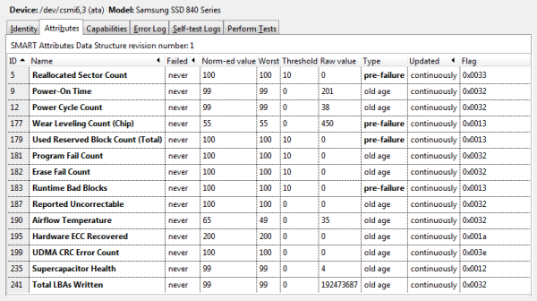
Note that if Samsung's WLC is anything like Intel's Media Wear Indicator, when the normalized counter value drops to 0 there's still a good amount of endurance actually left on the NAND (it could be as high as another 20 - 30%). At least with Intel drives, the MWI hitting 0 is a suggestion that you may want to think about replacing the drive and not a warning of imminent failure.
Conclusions
1,000 P/E cycles may not sound much but when it's put into perspective, it's still plenty. Client workloads rarely exceed 10GiB of writes per day on average and write amplification should stay within reasonable magnitudes as well:
Of course, if you write 20GiB a day, the estimated lifespan will be halved, although we are still looking at several years. Even with 30GiB of writes a day the 256GiB TLC drive should be sufficient in terms of endurance. Write amplification can also go over 10x if your workload is heavily random write centric, but that is more common in the enterprise side - client workloads are usually much lighter. SSD Lifetime Estimation NAND MLC—3K P/E Cycles TLC—1K P/E Cycles NAND Capacity 128GiB 256GiB 128GiB 256GiB Writes per Day 10GiB 10GiB 10GiB 10GiB Write Amplification 3x 3x 3x 3x Total Estimated Lifespan 35.0 years 70.1 years 11.7 years 23.4 years
Furthermore, it should be kept in mind that all SMART values that predict lifespan are conservative; it's highly unlikely that your drive will drop dead once the WLC or MWI hits zero. There is a great example at XtremeSystems where a 256GB Samsung SSD 830 is currently at nearly 5,000TiB of writes. Its WLC hit zero at 828TiB of writes, which means its endurance is over five times higher than what the SMART values predicted. That doesn't mean all drives are as durable but especially SSDs from NAND manufacturers (e.g. Intel, Crucial/Micron, Samsung etc.) seem to be more durable than what the SMART values and datasheets indicate, which isn't a surprise given that they can cherry-pick the highest quality NAND chips.

More...
-
11-16-12, 11:00 AM #2379
Anandtech: AnandTech/Intel S3700 Roundtable Discussion & Webcast Videos Live
Intel invited me to attend SC12 and participate in a webcast for the launch of its new DC S3700 SSD. I joined Roger Peene from Intel's SSD Solutions and we talked about the S3700 as well as answered your questions live. If you missed the webcast, you can find the pre-recorded video here. There's a great question about the future of NAND we discussed on the webcast that I'd highly recommend paying attention to.
Prior to the webcast, I had the chance to sit down with Arbin Kumar (responsible for Intel SSD reliability and validation), Allison Goodman (lead engineer on the S3700) and Roger Peene (Marketing Director for Intel's Datacenter SSD Solutions) once again to discuss the S3700 in greater detail. The discussion in the video below is from the first day I really learned about the S3700's architecture. The full discussion took several hours but the video below distills a lot of it down to 7 minutes. If you want to hear about the S3700 from the folks who actually had a hand in building the drive, I strongly suggest watching the video.
Finally, at SC12 Intel rented a replica of the original series bridge from the starship Enterprise which we used as a backdrop for the webcast. Prior to the webcast airing, we had some fun on the bridge which you can check out in the gallery below.
Gallery: The Starship Enterprise Bridge at SC12


At the end of the day it was a pretty fun experience. I learned quite a bit about Intel's NAND Solutions Group through this whole process. The SSD business is pretty unusual in that it's built around a replacement to a highly commoditized product (mechanical storage). It's surprising that we even have folks who typically play in high margin products even in this industry, but without them the market would be much worse off. I still remember what things were like with SSDs prior to the X25-M and even for the 12 - 18 months after its launch. The S3700 showed that there's still room for innovation even within the constraints of 6Gbps SATA, which should tide us over until SATA Express shows up.

More...
-
11-17-12, 01:30 PM #2380
Anandtech: Intel Explains 20nm NAND Endurance Concerns on the SSD 335
It's common knowledge by now that as NAND cells shrink in size (thanks to smaller process nodes), their endurance and program/erase latencies both suffer. Consumers wouldn't really be happy with newer drives dying sooner and performing worse than their predecessors, so controller and NAND makers have to work extra hard to compensate for losses due to the physics of NAND.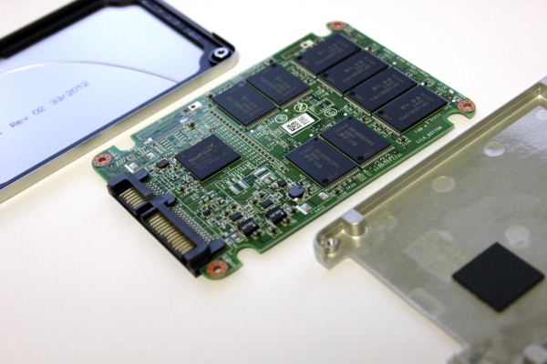
In the second half of this year we saw the beginning of a transition from Intel's 25nm MLC NAND to a 20nm process. The smaller process will eventually allow us to have larger SSDs with 16GB NAND die (up from the current 8GB max), but it should also help drive SSD prices down as you can fit more 20nm NAND cells per 300mm wafer than you can at 25nm. The cost motivation alone will move production from 25nm to 20nm in fairly short order. The question remains: how is endurance impacted by the move to 20nm? When Krisitian reviewed Intel's SSD 335, he tried to find out. 
The 335 is Intel's first branded drive to ship with 20nm 2-bit-per-cell MLC NAND. Like most modern Intel SSDs, the drive reports total NAND writes as well as the percent remaining program/erase cycles on the NAND. By looking at both values you can get a general idea of the expect lifespan of the NAND in number of program/erase cycles. 
In his 335 review, Kristian calculated the endurance of Intel's 20nm NAND on the 335 to be below 1,000 program/erase cycles. Intel confirmed that its 20nm MLC NAND is rated at 3,000 p/e cycles and that Kristian's results shouldn't have happened. Others duplicated the results around the web, so we waited for an explanation from Intel. Today we have that explanation.
The Media Wearout Indicator (MWI) on Intel SSDs looks at total number of times the drive's NAND has been cycled and then divides it by the p/e rating for the NAND to determine its value. The p/e rating is hard-coded into the firmware for the NAND. The 335 we reviewed had the p/e rating set to 1500 cycles, which was accurate for an earlier, non-production version of Intel's 20nm NAND. The 335 should have shipped with firmware that set this value to 3000 cycles, but someone forgot to set the variable to the right value in the firmware code. Woops. As a result, the MWI value on the 335 decreases at 2x the rate it should. This doesn't mean the drive is wearing out twice as fast as it should, just that the MWI data is inaccurate. Take our numbers from the 335 review and double them to get how long the 335 may last. 
Kristian's review showed that to be roughly 250TB of writes, which means the actual value is aroung 500TB of actual NAND writes (incompressible). Doing the math on the 240GB capacity gives us 2083 full drive writes over the life of the drive, or about 5.7 years of useful life if you write 240GB of data to the NAND every day. Even if your workload has a write amplification factor of 10x, you're still talking about 24GB of writes per day for nearly 6 years.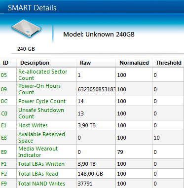
MWI from our 335 review, incorrectly low
The math works out to be around 1500 p/e cycles, however remember that when the MWI hits 0 the NAND isn't truly exhausted. It should last well beyond that point. The MWI hitting 0 on an Intel drive is just a good point to begin looking at replacing the drive.
Intel will have a firmware update for the 335 out before the end of the month that fixes the MWI reporting behavior, but if you're concerned about endurance on the 335 - I wouldn't be. 
There's another issue however. The 335 should have similar endurance to the 330, but even with our revised numbers the two look very different. It turns out MWI reporting on the 330 is not working at all; the MWI value will never drop, regardless of how much you write to the drive. Intel has committed to fixing this issue in a December firmware update for the 330.
Neither issue fundamentally impacts the functionality of the drive or its endurance. But if you're closely monitoring the MWI values, you should keep all of this in mind.
That's all for the Intel SSD update. I've been hearing more reports of dying Samsung SSD 840 Pros and I believe I know the cause (firmware related, should be fixed in the latest shipping revision) but I'm still waiting for confirmation on one last thing before explaining what's going on there.

More...


 Quote
QuoteThread Information
Users Browsing this Thread
There are currently 11 users browsing this thread. (0 members and 11 guests)


Bookmarks