

Results 2,381 to 2,390 of 12094
Thread: Anandtech News
-
11-18-12, 02:30 AM #2381
Anandtech: Qualcomm Begins Sampling MDM9x25 - Category 4 LTE, 3GPP Release 10
During an earnings conference call earlier this week, Qualcomm announced that it had begun sampling MDM9x25 to customers. MDM9x25 is Qualcomm's its third generation multimode 28nm baseband, the successor to MDM9x15, and also is Qualcomm's first UE Category 4 LTE baseband with 3GPP Release 10 support. Previous LTE basebands MDM9x00 (45nm) and MDM9x15 (28nm) were UE Category 3, which means a maximum of 100 Mbps of throughput on the downlink, even on 20 MHz wide LTE channels. Category 4 LTE modems will be able to use the full 100 resource blocks on 20 MHz FDD-LTE and thus see up to 150 Mbps of throughput, you just need a carrier that has 20 MHz FDD-LTE rolled out. In addition MDM9x25 will include support for LTE carrier aggregation inter-band and intra-band to aggregate together enough spectrum to get effectively 20MHz . 
In addition, MDM9x25's support for 3GPP Release 10 means inclusion of inter-band and intra-band carrier aggregation for WCDMA, in addition to MIMO support on top of DC-HSPA+. This means a theoretical bitrate of 84 Mbps for the carrier aggregation plus MIMO modes on WCDMA.
We have a lot more information about MDM9x25 and the current state of Qualcomm's upcoming modem and transceiver portfolio that we'll be going over in a larger piece in the coming week. Expect to see devices based on MDM9x25 start shipping sometime in 2013. 
Source: Qualcomm


More...
-
11-18-12, 07:30 PM #2382
Anandtech: Nintendo Wii U Teardown
When Nintendo announced the Wii U there was a lot of interest in its hardware specs. The new console could very well end up the fastest kid on the block thanks to the sheer age of the Xbox 360 and PlayStation 3. I wasn't all that interested in the Wii U, but I did want to get a look at the silicon inside so I grabbed a unit and went into teardown mode.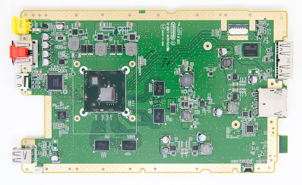
The Wii U is available in two versions: the basic and deluxe kits. The basic kit comes in white, while the deluxe is black. Both are glossy. The deluxe console gives you 32GB of on-board storage (eMMC NAND) vs. 8GB for the standard model. The deluxe kit also includes a stand and cradle for the Wii U tablet GamePad as well as a stand for the console itself. The two kits retail for $299.99 and $349.99, respectively.
The Wii U hardware itself looks a lot like a larger Wii. Getting inside the chassis is also quite similar. The CMOS battery door is the first thing you'll have to remove, followed by 8 more screws (a mixture of philips head and tri-tip). The bulk of these screws are behind console-colored stickers, be sure to peel them all off. With all 8 (9 including the CMOS battery door) screws removed, you can slide the left side of the Wii U away from the front of the console, and off all together. This reveals the final three tri-tip screws that you'll need to remove to get inside the chassis (the gallery of all of this is at the bottom of the article).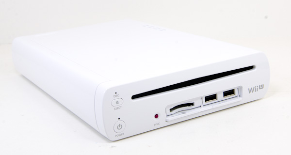
With all 12 screws removed, pry the top of the Wii U up and away from the body until it separates from the rest of the frame revealing the console's fairly compact internals:
The Wii U optical drive uses a custom format for game storage, but offers a very Blu-ray-like 25GB capacity per disc. Max sequential read speeds are pretty high compared to the current gen consoles at 22MB/s.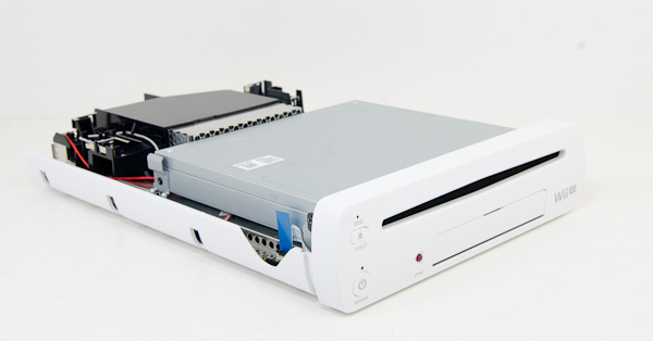
Two screws hold the front cover in place, followed by four screws that hold the optical drive in place. Be careful when removing the optical drive as there's a ribbon cable attached to the motherboard for power/data. The same goes for the front cover, although its ribbon cable is really only on light/switch duty.
With the optical drive removed, next up is removing the shielding on the top and bottom of the motherboard and the shround on top of the heatsink. Just go around the perimeter of the motherboard removing screws (you'll be able to remove all but two easily). Once you've done this, the motherboard will be able to separate from the Wii U's lower tray.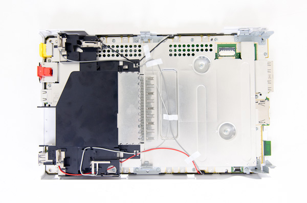
Removing the shielding itself requires carefully moving the antenna cables out of the way. As these wires are soldered to the Wii U chassis on one end, be very careful not to pull too hard otherwise you run the risk of needing to break out the soldering iron.
If you've removed all of the screws and freed the antenna wires from their guides a bit, you should be able to pull back the plastic heatsink shroud, revealing...more shielding:
With no screws left to hold it in place however, the shielding is easily dealt with (again pay close attention to the antenna wires). The same is true for the bottom of the PCB.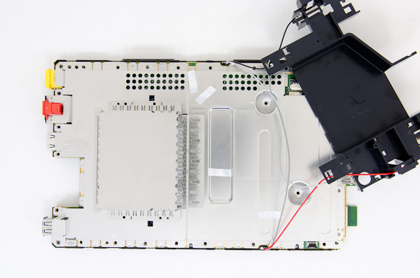
Once you've removed all shielding you're left with a pretty clean looking motherboard:
On the top side of the board you'll see the eMMC/NAND package, in this case it's a dual-die Samsung eMMC solution (there's another Toshiba NAND device on the back of the board, not for user storage):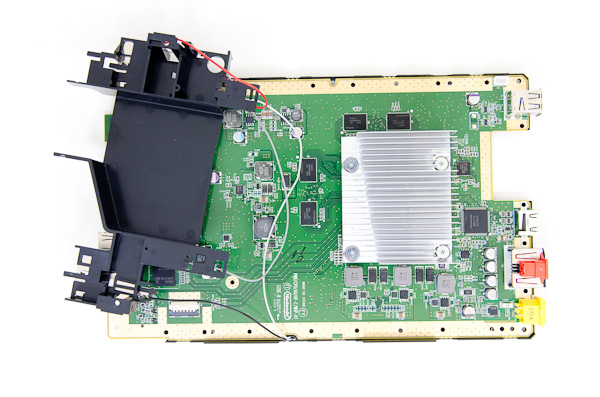
There are four 4Gb (512MB) Hynix DDR3-800 devices surrounding the Wii U's MCM (Multi Chip Module). Memory is shared between the CPU and GPU, and if I'm decoding the DRAM part numbers correctly it looks like these are 16-bit devices giving the Wii U a total of 6.4GB/s of peak memory bandwidth. That doesn't sound like a lot, but the Wii U is supposed to have a good amount of eDRAM for both the CPU and GPU to use.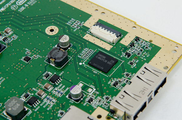
The Wii U's MCM is unfortunately covered by a heatspreader, but given that I went through all of this to look at the console's silicon, I was going to look at the console's silicon.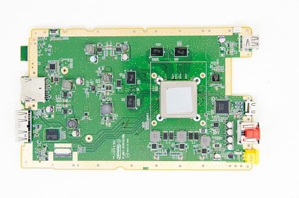
Normally to remove an integrated heat spreader (IHS) you grab a sharp blade and go around cutting the (hopefully) glue around the perimeter of the chip. In the case of the Wii U's MCM, the blades I'd normally use were too thick. A few years ago I decided to give shaving with a double edge safety razor a try. My attempts failed poorly, but I had a stack of unused DE razor blades that were thin enough to get the IHS off.
The trick here is to apply enough pressure to the blade to cut through the glue, as simply trying to saw through the glue will take forever. There are two blobs of glue per side, but if you're trying to remove the IHS be careful not to cut through the glue and scrape any of the actual exposed silicon...like I did.
With the IHS off, we have the Wii U's MCM in all of its glory:
There are actually three components on this single package, made in at least two different microprocessor fabs. The multicore PowerPC based CPU is the smaller of the two larger chips. This die is made on IBM's 45nm SOI process. The RV7xx derived GPU is the biggest die on the package, and I'm presuming it was made on a 40nm process. I'm assuming the very tiny die in the corner is actually some off-chip memory. Both the CPU and GPU in the Wii U are supposed to have some eDRAM, although the bulk of it is likely dedicated for the GPU.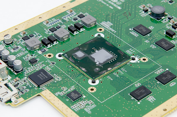
The approximate die sizes for all components on the MCM are in the table below: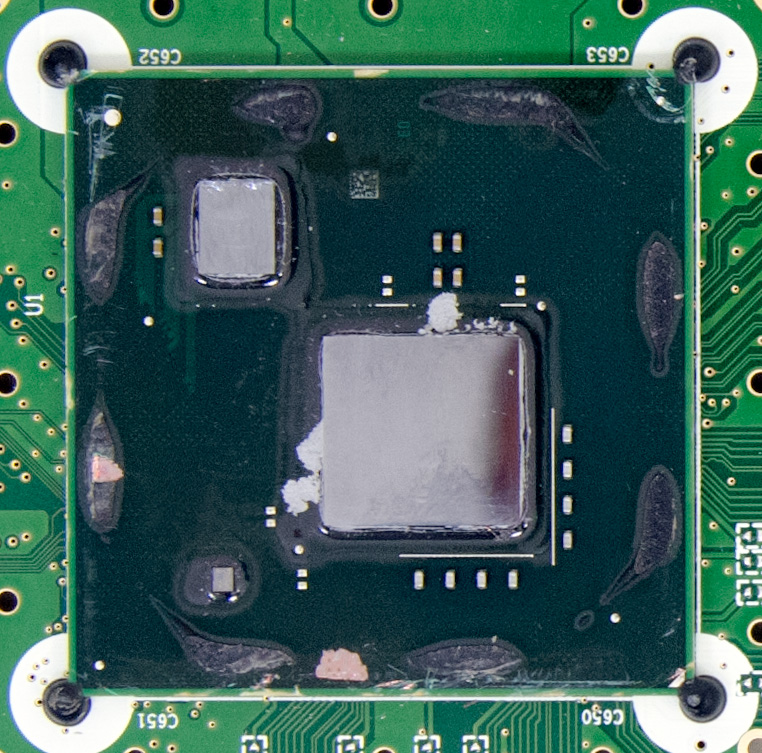
Clockwise from the top: CPU, GPU, off-chip memory?
If we assume a 40nm process for the GPU, then we're looking at something a bit larger than the RV740. The Wii U does boast backwards compatibility with games made for the original Wii, which is made possible thanks to a shared ISA with the original PowerPC based Wii.Wii U Silicon Analysis   Dimensions Approximate Die Size CPU 5.2mm x 6.3mm 32.76mm2 GPU 12.3mm x 12.7mm 156.21mm2 3rd die (memory?) 1.79mm x 1.48mm 2.65mm2
I've got some power consumption analysis I want to do, as well as look at visual quality on ports that also exist on the 360 but those will have to wait for now. Enjoy the gallery below of the entire teardown.

More...
-
11-19-12, 11:30 AM #2383
Anandtech: Habey Launches Fanless BIS-6922 and BIS-6636 Computers for Industrial Appl
Pursuant to our coverage of Aleutia's Relia fanless industrial PC, we received feedback from readers to provide more coverage for the industrial / embedded PC space. In this market, reliability and ruggedness are prime concerns. Habey USA (part of the NORCO group) has been in the industrial PC space since 1991. Recently, they have introduced two fanless PC models, one satisfying the requirements of the higher end market (where a lot of computing power is required), and the other for specialized embedded applications where the processing power provided by the Atom lineup is more than enough.
BIS-6922
The BIS-6922 is Habey's high-end offering with support for both Ivy Bridge and Sandy Bridge CPUs, using the QM77 / QM67 chipsets respectively. The units are passively cooled with Habey's custom ICEFIN technology. The motherboard itself has 2 SO-DIMM slots, two GbE LAN ports and a 2.5" HDD / SDD bay. In terms of expansion slots, we have 2x mini-PCIe, 1 x PCIe x16 and 1 x PCIe x4 connectors. Two simultaneous displays can be driven with the VGA, DVI-D, HDMI and 24-bit LVDS intefaces.
Gallery: Habey BIS-6922


Pricing varies from $416-455 for the barebones version (board and chassis), based on the quantity purchased. Full systems (including CPU, RAM and storage) are priced around $995 for an i3, $1195 for an i5 and around $1250 for an i7 CPU. Detailed specifications are provided below.
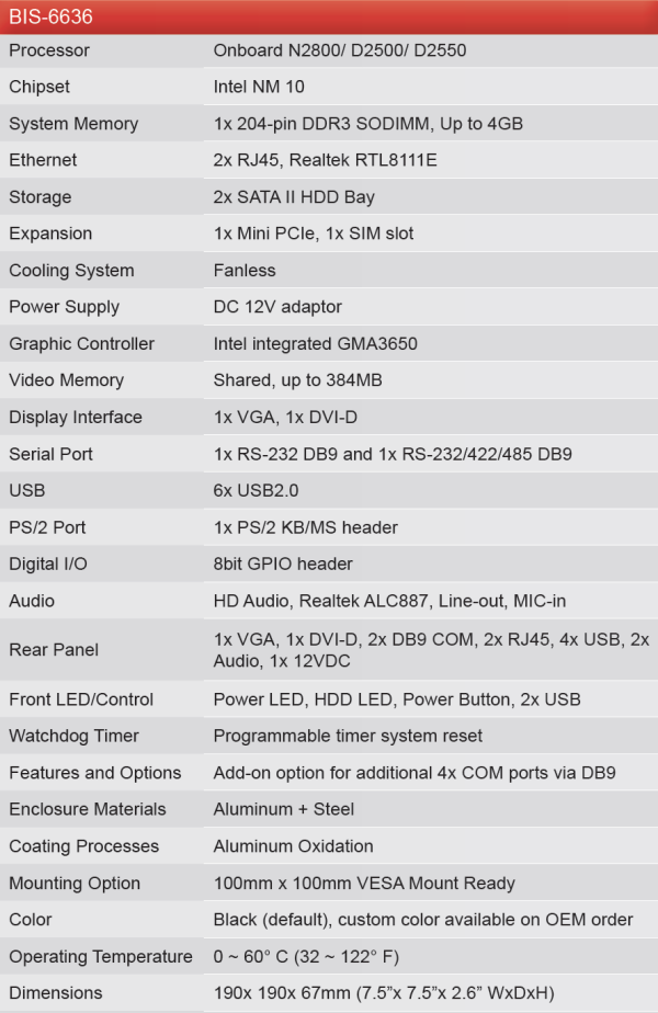
BIS-6636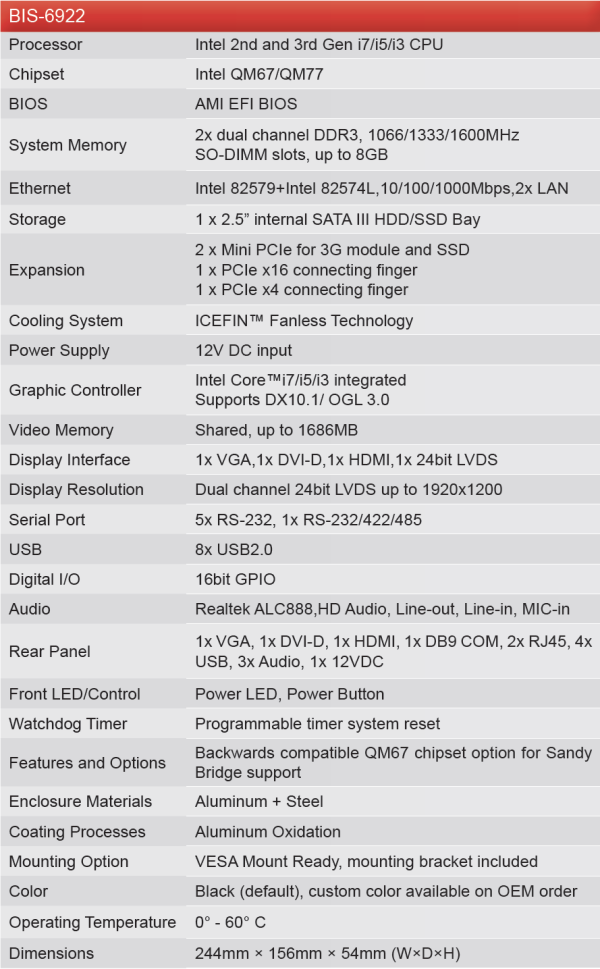
The BIS-6636 is a small form factor Intel Atom based system with dual NICs and up to 6 COM ports. Cedar Trail's PowerVR SGX545 GPU coupled with the VXD and VXE decoder and encoder engines allow Habey to advertise this unit for digital signage and NVR (networked video recorder) applications amongst other things. In terms oS support, we have drivers for Windows 7, Windows 7 Embedded and also embedded Linux OSes such as Timesys Fedora.
Gallery: BIS-6636


Pricing information is not available yet. Detailed specifications are provided below.

More...
-
11-19-12, 10:30 PM #2384
Anandtech: ASUS PB278Q Review: An IPS Competitor Emerges
Every 27” panel that I have reviewed this year has had two things in common: the panel was IPS based, and it was made by LG. The vast majority of IPS panels are made by LG, and so most high-end monitors use the same panels but have major differences in their electronics and design. In the past two years Samsung has entered the market with an alternative to IPS called PLS, or Plane-Line Switching.
While similar to IPS, PLS is designed to have advantages over traditional IPS. First, it has a higher level of transmittance, so more light gets through each individual cell. This allows you to use either a lower powered backlight, or to have a brighter display, both of which lower the power output required for a certain screen brightness. Second, as each cell allows more light though, you can pack them tighter allowing for displays with a higher pixel-per-inch count while keeping light output higher. PLS also claims to have better viewing angles for color and contrast in comparison to IPS. Let's see how the ASUS PB278Q fares in our testing.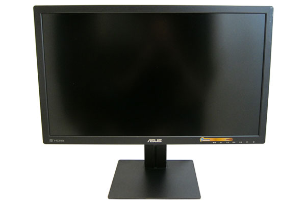

More...
-
Registered TeamPlayer

- Join Date
- 11-13-07
- Location
- Plano, TX and Ruston, LA
- Posts
- 32,364
- Post Thanks / Like

- Blog Entries
- 43
- Stat Links
-


- Gamer IDs
-

-
11-20-12, 10:30 AM #2386
Anandtech: AOC's i2367fh: Thin, Borderless, and IPS
We've been waiting for affordable LCDs to start showing some clear improvements in performance, quality, features, and design for a while. AOC has potentially done exactly that with their new i2367fh monitor, delivering an IPS-based panel with virtually no left/right or top borders. The bezel measures 2mm thick, making it a great option for multi-monitor users. It's currently available online starting at $189 (though it's also currently backordered).
Besides the thin bezel, the 23-inch i2367fh has WLED backlighting for the IPS panel, built-in speakers, VGA and two HDMI inputs to drive the 1080p display, and audio in/out ports. The stand doesn't appear to support any adjustments other than tilt, and there's no VESA mount, so this is definitely a niche product. However, it's a niche product that looks quite nice and should at least match what we've seen from TN panels for years at only a slight premium.
The display is so new AOC doesn't even list the i2367fh on their US/English sites yet, so the best information we can provide is via this ~7MB PDF, or if you prefer here's their Taiwan page. All we need now is for B&H to get more in stock (and for other resellers to show up). I don't know how others feel, but I'd love to see more displays ditch the 1" bezels—including on the bottom, please. There's nothing a thick bezel adds other than size, though obviously making a thin bezel does cost more.
Gallery: AOC's i2367fh: Thin, Borderless, and IPS


More...
-
11-20-12, 05:30 PM #2387
Anandtech: iPad mini Review
Over the last two months, Apple has updated almost all of its core product lines, with the addition of a 13” model to the Retina MacBook Pro line and new silicon for the iPad and Mac mini to go with ground up redesigns for the iPhone, iMac, iPod touch, and iPod nano. But the biggest story from the “little more” event was definitely the introduction of the iPad mini, a 7.9” counterpart to the 9.7” tablet that started it all.
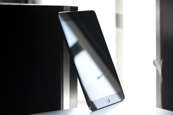
Read on for our full review of the second member of Apple's iPad family.

More...
-
11-21-12, 12:00 AM #2388
Anandtech: The AnandTech Podcast: Episode 10
We've made it to 10 episodes of the AnandTech Podcast! As promised, this week's episode is a bit more PC focused as we discuss the future of AMD. Intel's SSD DC S3700 is up for discussion, as well as the HPC space including the launch of Intel's Xeon Phi (baesd on the architecture formerly known as Larrabee). 
There's a bit of mobile discussion in the second half of the podcast, addressing TI's exit from the market and some final thoughts on the Nexus 4 from Brian.
The AnandTech Podcast - Episode 10
featuring Anand Shimpi, Brian Klug, Ryan Smith & Dr. Ian Cutress
iTunes
RSS - mp3, m4a
Direct Links - mp3, m4a
Total Time: 2 hours 8 minutes
Outline - hh:mm
Intel SSD DC S3700 and the Evolution of SSDs - 00:01
Intel's Xeon Phi - 00:16
AMD in the HPC Space - 00:41
AMD's Tough Times - 00:55
TI Exiting the Mobile SoC Business - 01:32
More on the Nexus 4 - 01:44
As always, comments are welcome and appreciated. 

More...
-
11-21-12, 02:30 PM #2389
Anandtech: Acer Aspire V5-171 Notebook Review: The Death and Rebirth of the Netbook
With all of the coverage we've done of ultrabooks in recent months, it's easy to forget that the big vendors are still out there plugging away with more basic, fundamental designs. Intel has expanded the definition of "ultrabook" enough that most consumer-grade systems being made available still fall into those categories, but ultraportables still bear a pretty substantial premium. At the same time, tablets coupled with the persistently dire performance of Atom have turned netbooks into a virtual flash in the pan.
There's a gap in the market that vendors like Acer, HP, and ASUS are quietly serving, though. It's clear from the way netbooks took off that consumers are interested in a small, inexpensive, portable notebook with just enough performance, and that's something you're not getting with ultrabooks. As you're going to see today, there's a lot to be gained if you're willing to sacrifice a little bit of Z-height. We have the Acer Aspire V5-171 on hand today. Acer is asking just $550 for an 11.6" notebook featuring an Ivy Bridge i5 ULV chip and 6GB of RAM, so what's the catch?.jpg)

More...
-
11-22-12, 12:30 PM #2390
Anandtech: Crucial v4 (256GB) Review
As with virtually all consumer electronics devices, there is market for various types and levels of SSD. Not everyone is ready to pay the premium for the fastest possible SSD but on the other hand, there are users who aren't ready to settle for products meant for the mainstream. Value SSDs have existed for years and we have seen various outcomes, some good and others not so good.
Today we're looking at Crucial's v4, the first value SSD from Crucial. Previously, Crucial's lineup has only consisted of one SSD at a time but that changed when Crucial launched the v4 but kept selling the faster m4 alongside. The v4 uses a somewhat unknown (at least for desktop SSDs) Phison PS3105 controller, which is in fact a SATA 3Gbps controller unlike most modern controllers. Read on to find out how the v4 performs and whether it's worth it to cheap out on an SSD.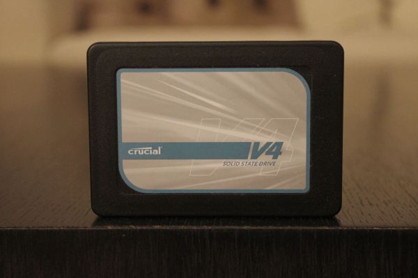

More...


 Quote
Quote


Thread Information
Users Browsing this Thread
There are currently 12 users browsing this thread. (0 members and 12 guests)


Bookmarks