

Results 2,961 to 2,970 of 12096
Thread: Anandtech News
-
06-01-13, 03:30 PM #2961
Anandtech: Intels Haswell: Quad-Core Desktop Processor SKUs
Intel’s Haswell is here, or at least the first salvo of quad-core parts has arrived. Just like we saw with Sandy Bridge and Ivy Bridge, Intel will be releasing Haswell in stages, starting at the high-end and trickling down from there. Today, we can tell you about the quad-core desktop and mobile parts, and we have several other articles going into greater detail on the performance and features you’ll get. These two Pipeline posts are going to strip out all the other stuff and just focus on the processors being launched today. We’ll have a few short tables showing the currently-announced quad-core SKUs for desktops and mobile, and we’ll have another similar post covering the dual-core parts when those are officially announced.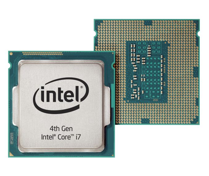
Starting at the top of the product and performance stack, we have the desktop Core i7 parts. All of these CPUs feature Hyper-Threading Technology, so they’re the same quad-core with four virtual cores that we’ve seen since Bloomfield hit the scene. The fastest chip for most purposes remains the K-series 4770K, with its unlocked multiplier and slightly higher base clock speed. Base core clocks as well as maximum Turbo Boost clocks are basically dictated by the TDP, with the 4770S being less likely to maintain maximum turbo most likely, and the 4770T and 4765T giving up quite a bit more in clock speed in order to hit substantially lower power targets.Intel 4th Gen Core i7 Desktop Processors Model Core i7-4770K Core i7-4770 Core i7-4770S Core i7-4770T Core i7-4770R Core i7-4765T Cores/Threads 4/8 4/8 4/8 4/8 4/8 4/8 CPU Base Freq 3.5 3.4 3.1 2.5 3.2 2.0 Max Turbo 3.9 (Unlocked) 3.9 3.9 3.7 3.9 3.0 Test TDP 84W 84W 65W 45W 65W 35W HD Graphics 4600 4600 4600 4600 Iris Pro 5200 4600 GPU Max Clock 1250 1200 1200 1200 1300 1200 L3 Cache 8MB 8MB 8MB 8MB 6MB 8MB DDR3 Support 1333/1600 1333/1600 1333/1600 1333/1600 1333/1600 1333/1600 vPro/TXT/VT-d/SIPP No Yes Yes Yes No Yes Package LGA-1150 LGA-1150 LGA-1150 LGA-1150 BGA LGA-1150 Price $339 $303 $303 $303 $303
It’s worth pointing out that the highest “Test TDP” values are up slightly relative to the last generation Ivy Bridge equivalents—84W instead of 77W. Whether that reflects a change in how they determine TDP or if it’s simply to give more headroom to the top performing parts isn’t clear. On the desktop, this is probably not particularly important—7W in TDP could often end up being just 1-2W in practice—so we’re not really concerned. Mobile TDPs are a different matter, and as we’ll discuss elsewhere they’re all 2W higher, but that could also be thanks in part to the higher performance iGPU.
Nearly all of these are GT2 graphics configurations (20 EUs), so they should be slightly faster than the last generation HD 4000 in graphics workloads. The one exception is the i7-4770R, which is also the only chip that comes in a BGA package. The reasoning here is simple, if flawed: if you want the fastest iGPU configuration (GT3e with 40 EUs and embedded DRAM), you’re probably not going to have a discrete GPU and will most likely be purchasing an OEM desktop. Interestingly, the 4770R also drops the L3 cache down to 6MB, and it’s not clear whether this is due to it having no real benefit (i.e. the eDRAM functions as an even larger L4 cache), or if it’s to reduce power use slightly, or Intel may have a separate die for this particular configuration. Then again, maybe Intel is just busily creating a bit of extra market segmentation.
Not included in the above table are all the common features to the entire Core i7 line: AVX instructions, Quick Sync, AES-NI, PCIe 3.0, and Virtualization Technology. As we’ve seen in the past, the K-series parts (and now the R-series as well) omit support for vPro, TXT, VT-d, and SIPP from the list. The 4770K is an enthusiast part with overclocking support, so that makes some sense, but the 4770R doesn’t really have the same qualification. Presumably it’s intended for the consumer market, as businesses are less likely to need the Iris Pro graphics.
The Core i5 lineup basically rehashes the above story, only now without Hyper-Threading. For many users, Core i5 is the sweet spot of price and performance, delivering nearly all the performance of the i7 models at 2/3 the price. There aren’t any Iris or Iris Pro Core i5 desktop parts, at least not yet, and all of the above CPUs are using the GT2 graphics configuration. As above, the K-series part also lacks vPro/TXT/VT-d support but comes with an unlocked multiplier.Intel 4th Gen Core i5 Desktop Processors Model Core i5-4670K Core i5-4670 Core i5-4670S Core i5-4670T Core i5-4570 Core i5-4570S Cores/Threads 4/4 4/4 4/4 4/4 4/4 4/4 CPU Base Freq 3.4 3.4 3.1 2.3 3.2 2.9 Max Turbo 3.8 (Unlocked) 3.8 3.8 3.3 3.6 3.6 Test TDP 84W 84W 65W 45W 84W 65W HD Graphics 4600 4600 4600 4600 4600 4600 GPU Max Clock 1200 1200 1200 1200 1150 1150 L3 Cache 6MB 6MB 6MB 6MB 6MB 6MB DDR3 Support 1333/1600 1333/1600 1333/1600 1333/1600 1333/1600 1333/1600 vPro/TXT/VT-d/SIPP No Yes Yes Yes Yes Yes Package LGA-1150 LGA-1150 LGA-1150 LGA-1150 LGA-1150 LGA-1150 Price $242 $213 $213 $213 $192 $192
Obviously we’re still missing all of the Core i3 parts, which are likely to be dual-core once more, along with some dual-core i5 parts as well. These are probably going to come in another quarter, or at least a month or two out, as there’s no real need for Intel to launch their lower cost parts right now. Similarly, we don’t have any Celeron or Pentium Haswell derivatives launching yet, and judging by the Ivy Bridge rollout I suspect it may be a couple quarters before Intel pushes out ultra-budget Haswell chips. For now, the Ivy Bridge Celeron/Pentium parts are likely as low as Intel wants to go down the food chain for their “big core” architectures.
For those interested in the mobile side of things, we’ve broken out those parts into a separate Pipeline article.
More...
-
06-01-13, 06:30 PM #2962
Anandtech: The Haswell Review: Intel Core i7-4770K & i5-4670K Tested
This is a very volatile time for Intel. In an ARM-less vacuum, Intel’s Haswell architecture would likely be the most amazing thing to happen to the tech industry in years. In mobile Haswell is slated to bring about the single largest improvement in battery life in Intel history. In graphics, Haswell completely redefines the expectations for processor graphics. There are even some versions that come with an on-package 128MB L4 cache. And on the desktop, Haswell is the epitome of polish and evolution of the Core microprocessor architecture. Everything is better, faster and more efficient.
More...
-
06-01-13, 07:00 PM #2963
Anandtech: Hit the Road, Jack: Intels Mobile Quad-Core Haswell SKUs
For those who are just looking for information on the various processor models with their associated features, we wanted to put together a short list of all the parts being launched today to go along with our architecture and performance testing (among other things). Similar to the previous two launches, Intel is starting off with their quad-core parts, to be followed at a later date by dual-core offerings. We’ll actually be going into the Ultrabook parts sooner rather than later, but for now there are no Core i3, Pentium, or Celeron Haswell chips. We’ve got a separate article going over the desktop SKUs, and our focus here will be on the mobile offerings.
On the mobile side of the fence, other than some slight changes to the naming scheme relative to Sandy Bridge and Ivy Bridge (there’s no more “20” suffix on most of the initial models and they’re now “MQ” instead of “QM”), the mobile Haswell rollout is what we expected. There are actually two quad-core mobile processor families, with the M-series being the “traditional” models while the H-series gets some iGPU upgrades and other tweaks.Intel 4th Gen Core i7 M-Series Mobile Processors Model Core i7-4930MX Core i7-4900MQ Core i7-4800MQ Core i7-4702MQ Core i7-4700MQ Cores/Threads 4/8 4/8 4/8 4/8 4/8 CPU Base Freq 3.0 2.8 2.7 2.2 2.4 Max SC Turbo 3.9 3.8 3.7 3.2 3.4 Max DC Turbo 3.8 3.7 3.6 3.1 3.3 Max QC Turbo 3.7 3.6 3.5 2.9 3.2 TDP 57W 47W 47W 37W 47W HD Graphics 4600 4600 4600 4600 4600 GPU Clock 400-1350 400-1300 400-1300 400-1150 400-1150 L3 Cache 8MB 8MB 6MB 6MB 6MB DDR3/DDR3L 1600 1600 1600 1600 1600 vPro/TXT/VT-d Yes Yes Yes No No Intel SBA No No No Yes Yes Price $1096 $568 $378
Along with the traditional Extreme part at the top of the hierarchy, we now get a 4900MQ, 4800MQ, and 4700MQ in place of the previous 3820QM, 3720QM, and 3610QM that we saw with Ivy Bridge. The 4800MQ, 4702MQ, and 4700MQ are 6MB L3 cache parts, so only the 4900MQ and 4930MX get the full 8MB L3. Other than the clock speed variations and the lack of vPro/TXT/VT-d on the 470x chips (which at the same time also get the distinction of being part of the Intel Small Business Advantage platform—basically, for non-managed networks), the parts all have HD 4600 Graphics. That means slightly better iGPU performance than HD 4000, but these are GT2 (20 EUs) rather than GT3/GT3e (40 EUs).
TDPs are up 2W relative to Ivy/Sandy Bridge models, but how that will actually play out in practice remains to be seen. Considering the max TDP is rarely hit under mobile workloads, we don’t expect any major changes, and Haswell is introducing a host of other improvements all aimed at delivering better battery life. Dustin has at least one Haswell notebook in for review, with a high-end CPU and dGPU. It won’t be a great representation of battery life, but at least we can get some idea of how much things have changed relative to the 3rd Generation Core i7 processors.
Here’s where things get interesting, the mobile H-Series processors. CPU clocks are down slightly relative to the above M-series, and all of these are 6MB L3 cache parts. To make up for that, Intel has equipped the top three HQ parts with their Iris Pro 5200 iGPU. While having faster integrated graphics may not really matter much on a desktop if you have a discrete GPU, on notebooks we generally always like having the faster iGPU available—you don’t always need a full discrete GPU for some tasks, but the cut-down GT1 of the previous generation sometimes fell short. Heat and noise are also more of a concern with notebooks, so running off the iGPU whenever possible is generally a good thing.Intel 4th Gen Core i7 H-Series Mobile Processors Model Core i7-4950HQ Core i7-4850HQ Core i7-4750HQ Core i7-4702HQ Core i7-4700HQ Cores/Threads 4/8 4/8 4/8 4/8 4/8 CPU Base Freq 2.4 2.3 2.0 2.2 2.4 Max SC Turbo 3.6 3.5 3.2 3.2 3.4 Max DC Turbo 3.5 3.4 3.1 3.1 3.3 Max QC Turbo 3.4 3.3 3.0 2.9 3.2 TDP 47W 47W 47W 37W 47W HD Graphics Iris Pro 5200 Iris Pro 5200 Iris Pro 5200 4600 4600 GPU Clock 200-1300 200-1300 200-1200 400-1150 400-1150 L3 Cache 6MB 6MB 6MB 6MB 6MB DDR3/DDR3L 1600 1600 1600 1600 1600 vPro/TXT/VT-d Yes Yes No No No Intel SBA No No Yes Yes Yes Price $657 $468
Intel has targeted roughly the level of performance offered by NVIDIA’s GT 650M with their Iris Pro 5200 graphics, or roughly a two-fold increase in performance over HD 4000, and that should be enough for everything short of high-quality, high-resolution gaming. What’s even more interesting is that there’s the potential for a reasonable gaming experience with the CPU and iGPU combined still drawing less than 47W of power; GT 650M may still be a better gaming chip, but the combined CPU + dGPU power draw is quite a bit higher than 47W. Of course, even on a 90Wh battery a load of 45W means you’d still get less than two hours of battery life. We’ll see about testing this as soon as we get more time with the hardware.
What I’m not quite getting is the role the 4702HQ and 4700HQ are supposed to fill; they’re still equipped with HD 4600 graphics, just like their MQ relatives, so we’ve asked Intel for clarification. Best guess right now: the MQ and HQ parts are different packages, so the 470xHQ chips are lower-echelon offerings for OEMs/users that don’t necessarily need/want Iris Pro 5200. It’s a way for an OEM to have one laptop that can support a range of processors, rather than locking all the HQ parts into higher-cost CPUs. Maybe down the road, we’ll even see some Core i5 H-Series CPUs, but we don’t have any concrete information on that yet.
For those interested in the desktop side of things, we’ve broken out those parts into a separate Pipeline article.
More...
-
06-02-13, 02:00 PM #2964
Anandtech: Exploring the Floating Point Performance of Modern ARM Processors
As a programmer who wants to write decent performing code, I am very interested in understanding the architectures of CPUs and GPUs. However, unlike desktop and server CPUs, mobile CPU and GPU vendors tend to do very little architectural disclosure - a fact that we've been working hard to change over the past few years. Often times all that's available are marketing slides with fuzzy performance claims. This situation frustrates me to no end personally. We've done quite a bit of low-level mobile CPU analysis at AnandTech in pursuit of understanding architectures where there is no publicly available documentation. In this spirit, I wrote a few synthetic tests to better understand the performance of current-gen ARM CPU cores without having to rely upon vendor supplied information. For this article I'm focusing exclusively on floating point performance.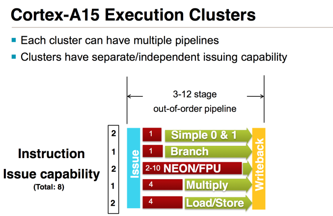
We will look at 5 CPU cores today: the ARM Cortex A9, ARM Cortex A15, Qualcomm Scorpion, Qualcomm Krait 200 and Qualcomm Krait 300. The test devices are listed below.
Device OS SoC CPU Frequency Number of cores Samsung Galaxy SIIX (T989D) Android 4.0 Qualcomm APQ8060 Scorpion 1.5GHz 2 Boundary devices BD-SL-i.mx6 Ubuntu Oneiric Freescale i.mx6 Cortex-A9 1.0GHz 4 Blackberry Z10 Blackberry 10 (10.1) Qualcomm MSM8960 Krait 200 1.5GHz 2 Google Nexus 10 Android 4.2.2 Samsung Exynos 5250 Cortex-A15 1.7GHz 2 HTC One Android 4.1.2 Qualcomm Snapdragon 600 Krait 300 1.7GHz 4
I wanted to test the instruction throughput of various floating point instructions. I wrote a simple benchmark consisting of a loop with a large number of iterations. The loop body consisted of many (say 20) floating point instructions with no data dependence between them. The tests were written in C++ with gcc NEON intrisincs where required, and I always checked the assembler to verify that the generated assembly was as expected. There were no memory instructions inside the loop and thus memory performance was not an issue. There were minimal dependencies in the loop body. I tested the performance of scalar addition, multiplication, multiply-accumulate and division for 32-bit and 64-bit floating point datatypes. All the tested ARM processors also support the NEON instruction set, which is a SIMD (single instruction multiple data) instruction set for ARM for integer and floating point operations. I tested the performance of 128-bit floating point NEON instructions for addition, multiplication and multiply-accumulate.
Apart from testing throughput of individual instructions, I also wrote a test for testing throughput of a program consisting of two types of instructions: scalar addition and scalar multiplication instructions. The instructions were interleaved, i.e. the program consisted of an addition followed by a multiply, followed by another add, then another multiply and so on. There were no dependencies between the additions and following multiplies. You may be wondering the reasoning behind this mixed test. Some CPU cores (such as AMD's K10 core) have two floating point units but the two floating point units may not be identical. For example, one floating point unit may only support addition while another may only support multiplication. Thus, if we only test the additions and multiplications separately, we will not see the peak throughput on such a machine. We perform the mixed test to identify such cases.
All the tests mentioned above measure the amount of time taken for a particular number of instructions and thus we get the instructions executed per-second. We also need to know the frequency to get the instructions executed per-cycle. Knowing the peak frequency of the device is not enough because CPUs have multiple frequency states and the tests may not be running at the advertised peak speeds. Thus, I also wrote code to monitor the percentage of time spent in each frequency state as reported by the kernel. The frequency was calculated as the average of the frequency states weighted by percentage of time spent in each state. The observed frequency on Scorpion (APQ8060) , Cortex A9 (i.mx6) and Cortex A15 (Exynos 5250) were 1.242 GHz, 992MHz and 1.7GHz respectively on all tests except where noted in the results below.
However, as it turns out, the method I used for measuring the time spent in each frequency state does not work on aSMP designs like the Krait 200 based Snapdragon S4 and Krait 300 based Snapdragon 600. For Krait 200, the results reported here are for MSM8960 which shouldn't really have thermal throttling issues. My results on the MSM8960 also line up quite neatly with the assumption that the CPU spent most or all of its time in the test in the peak frequency state. Brian also ran the test on a Nexus 4 and the results were essentially identical as both have the same peak, which is additional confirmation that our results are likely correct. Thus I will assume a frequency of 1.5 GHz while discussing Krait 200 results. Results on Krait 300 (Snapdragon 600) however are more mixed. I am not sure if it is reaching peak frequency on all the tests and thus I am less sure of the per-cycle estimates on this chip. Brian also ran the tests on another handset (LG Optimus G Pro) with the same Snapdragon 600, and the results very qualitatively similar.
Now the results. First up, the raw data collected from the tests in gigaflops:
Before we discuss the results, it is important to keep in mind that the results and per-cycle timing estimates reported are what I observed from the tests. I did my best to ensure that the design of the tests was very conducive to achieving high throughput. However, it is possible there may be some cases where an architecture can achieve higher performance than what what I was able to get out of my tests. With that out of the way, lets look at the results.Scorpion
(APQ8060)Cortex-A9
(i.mx6)Krait 200
(MSM8960)Cortex-A15
(Exynos 5250)Krait 300
(Snapdragon 600)Add (fp64) 1.23 0.99 1.33 1.55 @ 1.55 GHz 1.6 Add (fp32) 1.19 0.99 1.46 1.69 1.72 Mul (fp64) 0.61 0.50 1.48 1.69 1.72 Mul (fp32) 1.22 0.99 1.49 1.69 1.72 Mixed (fp64) 0.82 0.99 1.48 1.63 1.72 Mixed (fp32) 1.23 0.99 1.47 1.69 1.72 MAC (fp64) 1.23 0.99 1.48 3.35 2.65 MAC (fp32) 2.47 1.98 1.47 3.39 3.13 Add (fp32 NEON) 4.94 1.99 5.86 6.77 6.89 Mul (fp32 NEON) 4.89 1.99 5.76 6.77 6.89 MAC (fp32 NEON) 9.88 3.98 5.91 13.55 12.5
In the data, we need to distinguish between number of instructions and number of flops. I count scalar addition, multiply and division one flop and scalar MACs as two flops. I count NEON addition and multiply as four flops and NEON MACs are counted as eight flops. Thus, we get the following per-cycle instruction throughput estimates:
We start with the Cortex A9. Cortex A9 achieves throughput of 1 operation/cycle for most scalar instructions, except for fp64 MUL and fp64 MAC, which can only be issued once every two cycles. The mixed test reveals that though fp64 muls can only be issued every two cycles, Cortex A9 can issue a fp64 add in the otherwise empty pipeline slot. Thus, in the mixed test it was able to achieve throughput of 1 instruction/cycle. NEON implementation in Cortex A9 has a 64-bit datapath and all NEON instructions take 2 cycles. Qualcomm's Scorpion implementation of scalar implementations is similar to Cortex A9 except that it seems unable to issue fp64 adds immediately after fp64 muls in the mixed test. Scorpion uses a full 128-bit datapath for NEON and has twice the throughput of Cortex A9.Scorpion Cortex A9 Krait 200 Cortex A15 Krait 300 Add (fp64) 1 1 1 1 1 Add (fp32) 1 1 1 1 1 Mul (fp64) 1/2 1/2 1 1 1 Mul (fp32) 1 1 1 1 1 Mixed (fp64) 2/3 1 1 1 1 Mixed (fp32) 1 1 1 1 1 MAC (fp64) 1/2 1/2 1/2 1 7/9 MAC (fp32) 1 1 1/2 1 10/11 Add (fp32 NEON) 1 1/2 1 1 1 Mul (fp32 NEON) 1 1/2 1 1 1 MAC (fp32 NEON) 1 1/2 1/2 1 10/11
Krait 200 features an improved multiplier, and offers 1 instruction/cycle throughput for most scalar and NEON instructions. Interestingly, Krait 200 has half the per-cycle throughput for MAC instructions, which is a regression compared to Scorpion. Krait 300 improves the MAC throughput compared to Krait 200, but still appears to be unable to reach throughput of 1 instruction/cycle possibly revealing some issues in the pipeline. An alternate explanation is that Snapdragon 600 reduced the frequency in the MAC tests for some unknown reason. Without accurate frequency information, currently it is difficult to make that judgment. Cortex A15 is the clear leader here, and offers throughput of 1 FP instruction/cycle in all our tests.
In the big picture, readers may want to know how the the floating point capabilities of these cores compares to x86 cores. I consider Intel's Ivy Bridge and Haswell as datapoints for big x86 cores, and AMD Jaguar as a datapoint for a small x86 core. For double-precision (fp64), current ARM cores appear to be limited to 2 flops/cycle for FMAC-heavy workloads and 1 flops/cycle for non-FMAC workloads. Ivy Bridge can have a throughput of up to 8 flops/cycle and Haswell can do 16 flops/cycle with AVX2 instructions. Jaguar can execute up to 3 flops/cycle. Thus, current ARM cores are noticeably behind in this case. Apart from the usual reasons (power and area constraints, very client focused designs), current ARM cores also particularly lag behind in this case because currently NEON does not have vector instructions for fp64. ARMv8 ISA adds fp64 vector instructions and high performance implementations of the ISA such as Cortex A57 should begin to reduce the gap.
For fp32, Ivy Bridge can execute up to 16 fp32 flops/cycle, Haswell can do up to 32 fp32 flops/cycle and AMD's Jaguar can perform 8 fp32 flops/cycle. Current ARM cores can do up to 8 flops/cycle using NEON instructions. However, ARM NEON instructions are not IEEE 754 compliant, whereas SSE and AVX floating point instructions are IEEE 754 compliant. Thus, comparing flops obtained in NEON instructions to SSE instructions is not apples-to-apples comparison. Applications that require IEEE 754 compliant arithmetic cannot use NEON but more consumer oriented applications such as multimedia applications should be able to use NEON. Again, ARMv8 will fix this issue and will bring fully IEEE 754-compliant fp32 vector instructions.
To conclude, Cortex A15 clearly leads amongst the CPUs tested today with Krait 300 very close behind. It is also somewhat disappointing that none of the CPU cores tested displayed a throughput of more than 1 FP instruction/cycle in these tests. I end at a cautionary note that the tests here are synthetic tests that only stress the FP units. Floating point ALU peaks are only a part of a microarchitecture. Performance of real-world applications will depend upon rest of the microarchitecture such as cache hierarchy, out of order execution capabilities and so on. We will continue to make further investigations into these CPUs to understand them better.
More...
-
06-02-13, 04:30 PM #2965
Anandtech: Gigabyte's 8-Series Haswell Motherboard Tour [video]
Today is all about Haswell and Gigabyte is kicking things off with a video tour of some of their Haswell motherboard lineup. Colin from Gigabyte stopped by a couple of weeks back to show off some of the latest innovations implemented in Gigabyte's line of 8-series motherboards.
With Haswell the name of the game from the motherboard makers is really polish. With the exception of FIVR (Fully Integrated Voltage Regulator), the 8-series platform is very similar to those that came before it. This gave the motherboard makers time and encouragement to focus on improving user experience as much as possible. As a result we saw tons of attention paid to improving things like UEFI, software utilities and ease of use. Check out the video below to see what Gigabyte did this round.
More...
-
06-02-13, 05:30 PM #2966
Anandtech: Exploring the Floating Point Performance of Modern ARM Processors
As a programmer who wants to write decent performing code, I am very interested in understanding the architectures of CPUs and GPUs. However, unlike desktop and server CPUs, mobile CPU and GPU vendors tend to do very little architectural disclosure - a fact that we've been working hard to change over the past few years. Often times all that's available are marketing slides with fuzzy performance claims. This situation frustrates me to no end personally. We've done quite a bit of low-level mobile CPU analysis at AnandTech in pursuit of understanding architectures where there is no publicly available documentation. In this spirit, I wrote a few synthetic tests to better understand the performance of current-gen ARM CPU cores without having to rely upon vendor supplied information. For this article I'm focusing exclusively on floating point performance.
We will look at 5 CPU cores today: the ARM Cortex A9, ARM Cortex A15, Qualcomm Scorpion, Qualcomm Krait 200 and Qualcomm Krait 300. The test devices are listed below.
Device OS SoC CPU Frequency Number of cores Samsung Galaxy SIIX (T989D) Android 4.0 Qualcomm APQ8060 Scorpion 1.5GHz 2 Boundary devices BD-SL-i.mx6 Ubuntu Oneiric Freescale i.mx6 Cortex-A9 1.0GHz 4 Blackberry Z10 Blackberry 10 (10.1) Qualcomm MSM8960 Krait 200 1.5GHz 2 Google Nexus 10 Android 4.2.2 Samsung Exynos 5250 Cortex-A15 1.7GHz 2 HTC One Android 4.1.2 Qualcomm Snapdragon 600 Krait 300 1.7GHz 4
I wanted to test the instruction throughput of various floating point instructions. I wrote a simple benchmark consisting of a loop with a large number of iterations. The loop body consisted of many (say 20) floating point instructions with no data dependence between them. The tests were written in C++ with gcc NEON intrisincs where required, and I always checked the assembler to verify that the generated assembly was as expected. There were no memory instructions inside the loop and thus memory performance was not an issue. There were minimal dependencies in the loop body. I tested the performance of scalar addition, multiplication and multiply-accumulate for 32-bit and 64-bit floating point datatypes. All the tested ARM processors also support the NEON instruction set, which is a SIMD (single instruction multiple data) instruction set for ARM for integer and floating point operations. I tested the performance of 128-bit floating point NEON instructions for addition, multiplication and multiply-accumulate.
Apart from testing throughput of individual instructions, I also wrote a test for testing throughput of a program consisting of two types of instructions: scalar addition and scalar multiplication instructions. The instructions were interleaved, i.e. the program consisted of an addition followed by a multiply, followed by another add, then another multiply and so on. There were no dependencies between the additions and following multiplies. You may be wondering the reasoning behind this mixed test. Some CPU cores (such as AMD's K10 core) have two floating point units but the two floating point units may not be identical. For example, one floating point unit may only support addition while another may only support multiplication. Thus, if we only test the additions and multiplications separately, we will not see the peak throughput on such a machine. We perform the mixed test to identify such cases.
All the tests mentioned above measure the amount of time taken for a particular number of instructions and thus we get the instructions executed per-second. We also need to know the frequency to get the instructions executed per-cycle. Knowing the peak frequency of the device is not enough because CPUs have multiple frequency states and the tests may not be running at the advertised peak speeds. Thus, I also wrote code to monitor the percentage of time spent in each frequency state as reported by the kernel. The frequency was calculated as the average of the frequency states weighted by percentage of time spent in each state. The observed frequency on Scorpion (APQ8060) , Cortex A9 (i.mx6) and Cortex A15 (Exynos 5250) were 1.242 GHz, 992MHz and 1.7GHz respectively on all tests except where noted in the results below.
However, as it turns out, the method I used for measuring the time spent in each frequency state does not work on aSMP designs like the Krait 200 based Snapdragon S4 and Krait 300 based Snapdragon 600. For Krait 200, the results reported here are for MSM8960 which shouldn't really have thermal throttling issues. My results on the MSM8960 also line up quite neatly with the assumption that the CPU spent most or all of its time in the test in the peak frequency state. Brian also ran the test on a Nexus 4 and the results were essentially identical as both have the same peak, which is additional confirmation that our results are likely correct. Thus I will assume a frequency of 1.5 GHz while discussing Krait 200 results. Results on Krait 300 (Snapdragon 600) however are more mixed. I am not sure if it is reaching peak frequency on all the tests and thus I am less sure of the per-cycle estimates on this chip. Brian also ran the tests on another handset (LG Optimus G Pro) with the same Snapdragon 600, and the results were qualitatively very similar.
Now the results. First up, the raw data collected from the tests in gigaflops:
Before we discuss the results, it is important to keep in mind that the results and per-cycle timing estimates reported are what I observed from the tests. I did my best to ensure that the design of the tests was very conducive to achieving high throughput. However, it is possible there may be some cases where an architecture can achieve higher performance than what what I was able to get out of my tests. With that out of the way, lets look at the results.Scorpion
(APQ8060)Cortex-A9
(i.mx6)Krait 200
(MSM8960)Cortex-A15
(Exynos 5250)Krait 300
(Snapdragon 600)Add (fp64) 1.23 0.99 1.33 1.55 @ 1.55 GHz 1.6 Add (fp32) 1.19 0.99 1.46 1.69 1.72 Mul (fp64) 0.61 0.50 1.48 1.69 1.72 Mul (fp32) 1.22 0.99 1.49 1.69 1.72 Mixed (fp64) 0.82 0.99 1.48 1.63 1.72 Mixed (fp32) 1.23 0.99 1.47 1.69 1.72 MAC (fp64) 1.23 0.99 1.48 3.35 2.65 MAC (fp32) 2.47 1.98 1.47 3.39 3.13 Add (fp32 NEON) 4.94 1.99 5.86 6.77 6.89 Mul (fp32 NEON) 4.89 1.99 5.76 6.77 6.89 MAC (fp32 NEON) 9.88 3.98 5.91 13.55 12.5
In the data, we need to distinguish between number of instructions and number of flops. I count scalar addition and multiply as one flop and scalar MACs as two flops. I count NEON addition and multiply as four flops and NEON MACs are counted as eight flops. Thus, we get the following per-cycle instruction throughput estimates:
We start with the Cortex A9. Cortex A9 achieves throughput of 1 operation/cycle for most scalar instructions, except for fp64 MUL and fp64 MAC, which can only be issued once every two cycles. The mixed test reveals that though fp64 muls can only be issued every two cycles, Cortex A9 can issue a fp64 add in the otherwise empty pipeline slot. Thus, in the mixed test it was able to achieve throughput of 1 instruction/cycle. NEON implementation in Cortex A9 has a 64-bit datapath and all NEON instructions take 2 cycles. Qualcomm's Scorpion implementation of scalar implementations is similar to Cortex A9 except that it seems unable to issue fp64 adds immediately after fp64 muls in the mixed test. Scorpion uses a full 128-bit datapath for NEON and has twice the throughput of Cortex A9.Scorpion Cortex A9 Krait 200 Cortex A15 Krait 300 Add (fp64) 1 1 1 1 1 Add (fp32) 1 1 1 1 1 Mul (fp64) 1/2 1/2 1 1 1 Mul (fp32) 1 1 1 1 1 Mixed (fp64) 2/3 1 1 1 1 Mixed (fp32) 1 1 1 1 1 MAC (fp64) 1/2 1/2 1/2 1 7/9 MAC (fp32) 1 1 1/2 1 10/11 Add (fp32 NEON) 1 1/2 1 1 1 Mul (fp32 NEON) 1 1/2 1 1 1 MAC (fp32 NEON) 1 1/2 1/2 1 10/11
Krait 200 features an improved multiplier, and offers 1 instruction/cycle throughput for most scalar and NEON instructions. Interestingly, Krait 200 has half the per-cycle throughput for MAC instructions, which is a regression compared to Scorpion. Krait 300 improves the MAC throughput compared to Krait 200, but still appears to be unable to reach throughput of 1 instruction/cycle possibly revealing some issues in the pipeline. An alternate explanation is that Snapdragon 600 reduced the frequency in the MAC tests for some unknown reason. Without accurate frequency information, currently it is difficult to make that judgment. Cortex A15 is the clear leader here, and offers throughput of 1 FP instruction/cycle in all our tests.
In the big picture, readers may want to know how the the floating point capabilities of these cores compares to x86 cores. I consider Intel's Ivy Bridge and Haswell as datapoints for big x86 cores, and AMD Jaguar as a datapoint for a small x86 core. For double-precision (fp64), current ARM cores appear to be limited to 2 flops/cycle for FMAC-heavy workloads and 1 flops/cycle for non-FMAC workloads. Ivy Bridge can have a throughput of up to 8 flops/cycle and Haswell can do 16 flops/cycle with AVX2 instructions. Jaguar can execute up to 3 flops/cycle. Thus, current ARM cores are noticeably behind in this case. Apart from the usual reasons (power and area constraints, very client focused designs), current ARM cores also particularly lag behind in this case because currently NEON does not have vector instructions for fp64. ARMv8 ISA adds fp64 vector instructions and high performance implementations of the ISA such as Cortex A57 should begin to reduce the gap.
For fp32, Ivy Bridge can execute up to 16 fp32 flops/cycle, Haswell can do up to 32 fp32 flops/cycle and AMD's Jaguar can perform 8 fp32 flops/cycle. Current ARM cores can do up to 8 flops/cycle using NEON instructions. However, ARM NEON instructions are not IEEE 754 compliant, whereas SSE and AVX floating point instructions are IEEE 754 compliant. Thus, comparing flops obtained in NEON instructions to SSE instructions is not apples-to-apples comparison. Applications that require IEEE 754 compliant arithmetic cannot use NEON but more consumer oriented applications such as multimedia applications should be able to use NEON. Again, ARMv8 will fix this issue and will bring fully IEEE 754-compliant fp32 vector instructions.
To conclude, Cortex A15 clearly leads amongst the CPUs tested today with Krait 300 very close behind. It is also somewhat disappointing that none of the CPU cores tested displayed a throughput of more than 1 FP instruction/cycle in these tests. I end at a cautionary note that the tests here are synthetic tests that only stress the FP units. Floating point ALU peaks are only a part of a microarchitecture. Performance of real-world applications will depend upon rest of the microarchitecture such as cache hierarchy, out of order execution capabilities and so on. We will continue to make further investigations into these CPUs to understand them better.
More...
-
06-02-13, 07:30 PM #2967
Anandtech: Intel's Haswell - An HTPC Perspective: Media Playback, 4K and QuickSync Ev
Over the last two years, the launch of every major desktop CPU family from both AMD and Intel has been accompanied by a dedicated HTPC-oriented article. This coverage has been complementary to Anand's extensive analysis from a general computing perspective. Haswell will be no different.
The advancements made from Llano to Trinity and from Sandy Bridge to Ivy Bridge had rendered entry level platforms good enough for casual / mainstream HTPC users. Advanced users still require discrete GPUs for using some video renderers and obtaining accurate display refresh rates. Each vendor has their own quirks when it comes to driver features and stability. This has made it difficult to declare any one solution as the perfect HTPC platform. Intel has hyped up improved GPU performance in the lead up to Haswell. Does it do enough to make the discrete GPU redundant for HTPCs? Read on to find out.
More...
-
06-02-13, 08:00 PM #2968
Anandtech: Gigabyte Launching Two New Haswell Xeon Server Motherboards
On the back of the Haswell launch a Gigabyte email dropped in our inbox regarding a pair of new single socket workstation motherboards they are launching for Haswell Xeons. Asides from the IPC gain of Haswell, the new Intel NIC as well as TSX are primary components for upgrading.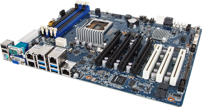
First up is the GA-6LXSV, a tower and rack capable ATX motherboard featuring Intel’s C224 chipset, support for up to 32GB of ECC/nonECC, and quad Intel gigabit Ethernet (I210).
Aside from the integrated ASpeed AST2300 2D display adaptor, we have PCIe slots all bunched up in a PCIe 3.0x x16/x8/x4 arrangement followed by a PCIe 2.0 x1 from the chipset, and a trio of PCI slots. SATA connectivity is also a little different to other Haswell products, with four SATA 6 Gbps and two SATA 3 Gbps on board. We also get an integrated USB port for software validation dongles inside the chassis.
Next up is a motherboard clearly named by a northern British designer, being called the GA-LASS. This is a micro-ATX motherboard for compact systems, again listed as both for rack and tower. By contrast to the GA-6LXSV, the connectivity is significantly reduced – a single Intel NIC, two SATA 6 Gbps, four SATA 3 Gbps and a single PCIe 3.0 x16.
There is also a PCIe 2.0 x4 and a pair of PCIe 2.0 x1 (one in an x4 width slot) and a USB 2.0 port on the motherboard. Like the larger model, memory support is for ECC and non-ECC modules, but limited to 32 GB.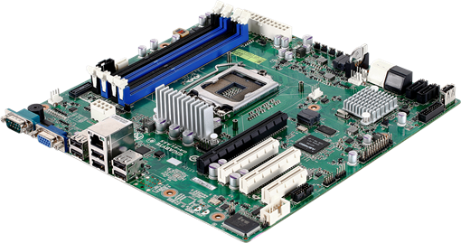
Specific launch dates and pricing are as yet unannounced. Typically Gigabyte server boards do not enter general sale, but with enough interest we might see some cropping up on official e-tailers. System integrators should get in contact with their local Gigabyte server sales team for information.
Over recent months we have had a look at a couple of Gigabyte’s motherboard server range, and I am speaking to their Server guys this week while in Computex. Is there any particular model anyone would like to see reviewed at AnandTech?
More...
-
06-02-13, 11:00 PM #2969
Anandtech: ARM Cortex A12: Between Cortex A9 and A15 in Power & Perf, Sampling in Lat
We’ve talked about the hole in ARM’s product lineup for quite a while now. The Cortex A9 is too slow to compete with the likes of Intel’s Atom and Qualcomm’s Krait 200/300 based SoCs. The Cortex A15 on the other hand outperforms both of those solutions, but at considerably higher power and die area requirements. The slide below from Samsung illustrates my point clearly: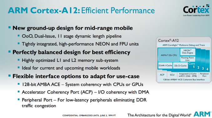

The comparison point here is the Cortex A15 and Cortex A7, but the latter should be quite performance competitive with a Cortex A9 so the comparison is still relevant. The Cortex A15 island in Samsung’s Exynos 5 Octa occupies 5x the die area as the A7 island, and consumes nearly 6x the power. In exchange for 5x the area and 6x the performance, the Cortex A15 offers under 4x the performance. It’s not exactly an area or power efficient solution, but a great option for anyone looking to push the performance envelope.
Today, ARM is addressing that hole with the Cortex A12.
This announcement isn’t a deep architectural disclosure, but we do have some high level details to share. Like AMD’s Jaguar, Intel’s Silvermont and even ARM’s A9, the Cortex A12 is a dual-issue out-of-order architecture. Unlike the Cortex A9, the Cortex A12 is fully out-of-order including the NEON/FP units (NEON/FP was in-order on Cortex A9).
Pipeline length increased a bit compared to Cortex A9 (11 stages), however ARM told me to expect similar frequencies to what we have with the Cortex A9.
The execution back end has also been improved, although I don’t have many details as to how. My guess is we should expect something a bit wider than Cortex A9 but not nearly as wide as Cortex A15.
Memory performance is much improved compared to Cortex A9 as well, which we’ve already demonstrated as a significant weak point in the A9 architecture.
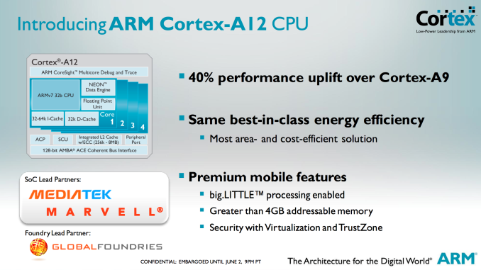
All of the architectural enhancements are supposed to provide up to a 40% increase in performance (IPC) over Cortex A9 at the same frequency and process node. ARM isn’t talking power, other than to say that it can do the same workload at the same power as a Cortex A9. In order words, Cortex A12 should have higher power than Cortex A9 but faster execution reduces total energy consumed. With a higher max power we’ll see more dynamic range in power consumption, but just not nearly as much as with the Cortex A15.
Cortex A12 also adds support for 40-bit memory addressability, an intermediate solution before we get to 64-bit ARMv8 based architectures. Finally, Cortex A12 features the same ACE bus interface as Cortex A7/A15 and can thus be used in big.LITTLE configurations with either core (but likely exclusively with the A7s). Given the lower power profile of Cortex A12, I'm not sure the complexity of doing a big.LITTLE implementation will be worth it though.

ARM expects the Cortex A12 to be used in mainstream smartphones and tablets where cost and power consumption are a bit more important. The design makes a lot of sense, the only downside is its launch timeframe. ARM expects to be sampling Cortex A12 in late 2014 with the first devices showing up in 2015. ARM has optimized Cortex A12 processor packs at both Global Foundries (28nm SLP) and TSMC (28nm HPM).

More...
-
06-02-13, 11:00 PM #2970
Anandtech: ARM Mali-T622 & V500 Video Block Complement Cortex A12
Alongside today's Cortex A12 announcement, ARM is also announcing two new IP blocks: the Mali-T622 GPU and the Mali V500 video encode/decode block.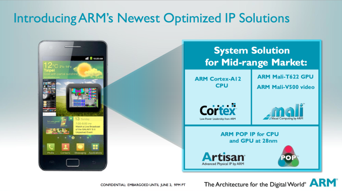
The Mali-T622 is a 2-core implementation of the 2nd generation Mali-T600 GPU architecture that we first learned about with the 8-core T628. Each shader core features two ALUs, an LSU and a texture unit.

On the video front, the Mali-V500 video encode/decode block is a multi-core engine used for all video acceleration. The V500 allegedly supports up to 100Mbps High Profile H.264, although details are scarce on more specifics. ARM claims support for up to 120 fps 4K video decode with an 8-core V500 implementation. Mali-V500 also features a protected video path, necessary for gaining content owner support for high-bitrate/high-resolution video decode.

The V500 also supports ARM's Frame Buffer Compression (AFBC), a lossless compression algorithm that can supposedly reduce memory bandwidth traffic by up to 50%. There's presently no frame buffer compression in Mali GPUs today, but ARM expects to eventually roll AFBC out to Mali GPUs as well.
Gallery: ARM Mali-T622 & V500 Video Block Complement Cortex A12


More...


 Quote
QuoteThread Information
Users Browsing this Thread
There are currently 8 users browsing this thread. (0 members and 8 guests)


Bookmarks