

Results 3,231 to 3,240 of 12096
Thread: Anandtech News
-
08-16-13, 09:00 AM #3231
Anandtech: A Tour of Moto Maker: Customization Meets the Moto X
A key part of the Moto X's story is one of hardware customization. At launch, those users buying Moto Xes on AT&T will be given the option of selecting from 18 back colors, 2 front colors and 7 accent colors. Additional options include custom text on the back of your device, storage capacity (16GB or 32GB), charger color, cases and headphones. It works out to around 504 different possible combinations of Moto X choices users can select from. I won't go into great detail on the Moto X here as Brian has already done a great job of that in his original piece, and we have a full review in the works.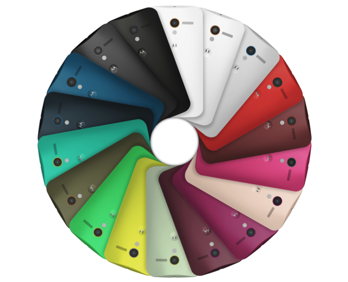
If you show up at an AT&T store, you'll be able to see examples of color combinations in person, but you can only go home with a woven white or woven black model. This is the composite material, carbon fiber-looking back we've shown photos of already, with a matching black or white front. If you want to customize a Moto X, you can buy a Moto X redemption card - good for one customized Moto X. Take the redemption card home, head to motorola.com/designit, type in your PIN and off you go. The AT&T store visit is purely optional however, you can just go to motomaker.com and buy a fully customized Moto X directly from Motorola.
In both cases, the Moto X receives final customization and assembly in Fort Worth, Texas. The process should take approximately 4 days depending on component availability. If you don't like what you end up with, you're free to exchange/return the device within a 14-day window.
Motorola provided us with PIN codes to try out the nearly-final version of Moto Maker and pick out our own custom Moto X design options. Brian put together an excellent video taking you through the entire process:
There are a few minor bugs/inconsistencies in the Moto Maker webapp itself but otherwise the process is quite painless. It's pretty easy to tell what color combinations work or don't work, and Motorola has a number of recommendations for designs already made. As with any online configurator, image accuracy is always a concern. We won't see the results of our customizations for a few days, but we'll do a follow-up post comparing what Moto Maker presented us with and what it looks like in person.
At present the options include the different colored backs which are polymer, in addition to the two woven composite materials. Other patterns will gradually be made available, along with the wood back options that we were shown, although Motorola still doesn't have specific timing beyond saying sometime in the Q4 timeframe for those wood options.
It took me much longer than I expected to settle on a color combination. There aren't an overwhelming number of choices, but there are enough options to make you think - and a number of really good looking combinations. I found it very easy to put together a fairly subtle phone with a splash of color thanks to the 7 accent colors, but I ultimately ended up designing something pretty over the top – lemon lime with yellow accents and the white front. Brian settled on olive with silver accents and the white front.
There is a small amount of software customization that comes with Moto Maker. Based on the color you choose for the back of the Moto X, Motorola will pre-select a wallpaper that matches. You can specify custom text to be displayed at boot, and finally you can opt to automatically setup your Google account on the phone to simplify the out of box experience when you finally get it.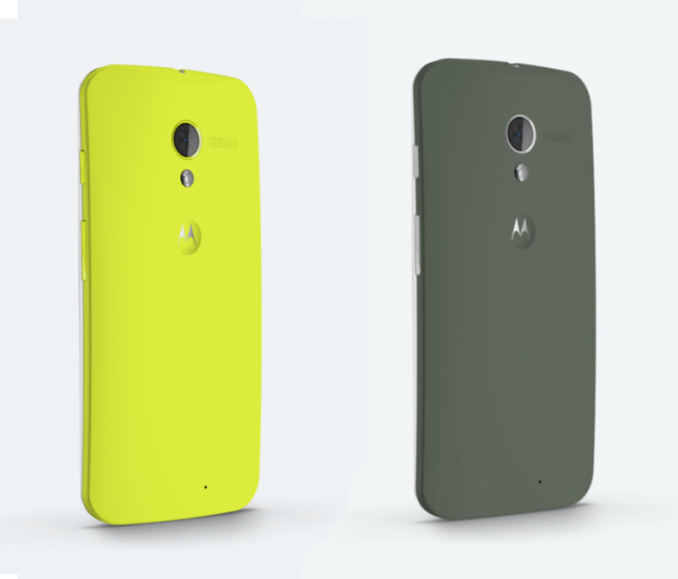
The purchase experience is something that we rarely talk about in our reviews, but it does play a major role in customer satisfaction. I feel like Moto Maker is a successful attempt to improve the smartphone purchasing process. The customization options are easy to get excited about, and the overall experience is without equal in the phone space today. Given how personal these smartphones are, the customization play with Moto Maker is clearly very well thought out. As we've seen in the past though, personalization alone isn't enough to make for a successful product. Stay tuned for our full review of the Moto X.
Gallery: Moto X: Moto Maker


More...
-
08-16-13, 02:30 PM #3232
Anandtech: Humble Bundle: Origin Edition
Over the years we’ve seen a variety of games offered up on the Humble Bundle; some have been pretty ho-hum, while others have been well worth the price of admission. Of course, the price of admission now is practically free: it’s whatever you want, starting at a whopping $0.01 – yes, an entire penny for the Humble Bundle. The latest version comes courtesy of EA’s Origin, rather than the usual Steam codes, and you get six games that range from okay to unappreciated gems to major blockbusters.
Any contribution will get you all six of the following games; I’ve included the current retail (Origin) pricing on each as a reference point: Burnout Paradise: The Ultimate Box ($19.99), Crysis 2 Maximum Edition ($29.99), the original Dead Space ($19.99), the latest Dead Space 3 sequel ($39.99), Mirror’s Edge ($19.99), and Medal of Honor ($19.99). So if you were to buy just those six games off of Origin right now, you’d be paying nearly $150 – not that I’d suggest you do so, but if you’ve missed any of them and are looking for a diversion, they’re not bad.
As an added bonus, if you pay more than the current average Humble Bundle price ($4.80 at the time of writing), you get two additional titles. Battlefield 3 ($19.99) hardly needs an introduction, and the same goes for The Sims 3 (Starter Pack – $29.99). The Starter Pack comes with the main game as well as the High-End Loft and Late Night expansion packs. So, less than $5 can currently net you eight games, most of which are worth a look.
The hook for the Humble Bundle is that you get to choose how your contribution is distributed. You can given any percentage to one of five charities (Human Rights Campaign, Watsi, San Francisco AIDS Foundation, American Cancer Society, and American Red Cross), or you can give a “Humble Tip” to the Humble Bundle people for their time and bandwidth involved with the promotion. You can also gift the purchase to someone else if you like.
Of course there’s always a catch, right? Sure, and this time it’s pretty simple: some of the games as you might have guessed have to be used through EA’s Origin service. Now, I didn’t much care for the initial launch of the EA Downloader, which later became Origin, but things have at least improved. I don’t know that it’s equal to Steam, as transferring games between computers is a bit more of a pain, but it’s not terrible at least. Of the eight titles, three are only available with Origin (Battlefield 3, Dead Space 3, and The Sims 3 – these things come in threes or something?); the other five games can be used with either Steam or Origin – or even both! How’s that for generous?
Note that you redeem the codes for the Sims 3 through the Sims 3 web page, but the instructions from EA for redeeming the expansion packs are incorrect: you need to redeem those through Origin. At least when I did it, the Sims 3 My Store Account section has “Redeem a Code”, but it only has blocks for four parts of the code, and my codes were five blocks of four characters. Oops. There was also some sluggishness with Origin as I was writing this, perhaps caused by a deluge of Humble Bundle downloads.
However you want to look at it, for practically free you can enjoy some of the past three or four years of gaming action. That’s a price that’s hard to beat, and hey: it’s for charity, so feel free to be generous! There are currently just under 12 days remaining on this offer.
More...
-
08-16-13, 09:30 PM #3233
Anandtech: Gigabyte Announces FM2+ A88X Series Motherboards for Kaveri
The evolution of the Bulldozer module, through Piledriver, and Steamroller on Kaveri to come has been an eventful journey. Despite recent rumors floating around the Internet reporting delays to AMD’s deployment of Kaveri (which AMD have since confirmed to the media that Kaveri will ship in Q4-2013), motherboard manufacturers, like GIGABYTE, are announcing their lineup for Steamroller based APUs.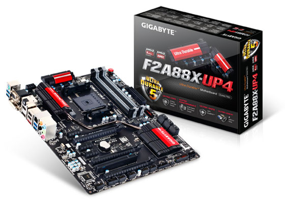
These APUs will be using the FM2+ socket, which is backwards compatible with Trinity/Richland FM2 APUs (FM2 based motherboards are not forwards compatible), as well as a new chipset in the form of A88X, which as far as we know is for FM2+ only. These new APUs offer native support for PCIe 3.0 as well as DX11.1 and 4K support – something all AMD partners will be keen to promote.
GIGABYTE’s initial FM2+ lineup will consist of seven models with four ATX and three micro-ATX:
G1.Sniper A88X
F2A88X-UP4
F2A88X-D3H
F2A88X-HD3
F2A88XM-D3H
F2A85XM-DS2
F2A88XM-HD3
Continuing on the Sniper theme, the G1.Sniper A88X is aimed at the gaming market with two new exclusive audio features – GIGABYTE USB DAC-UP (a feature for optimized power to user DACs) and Gain Boost where high gain output is required. This board will also feature the high end audio solution from the G1.Sniper 5 (the Intel Z87 version), including OP-AMP, audio tracing separation and filter caps to improve noise quality. Below the G1.Sniper A88X is the F2A88X-UP4, which will feature 60A IR3550 ICs in its power delivery, similar to the F2A85X-UP4 which we reviewed in our initial Trinity coverage.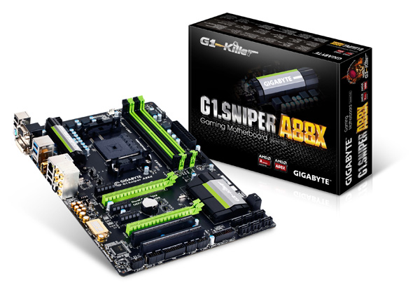
Release date for these motherboards is likely to be the same day that AMD release Kaveri, which should be in the hands of system integrators by the end of the year.
Gallery: Gigabyte Announces FM2+ A88X Series Motherboards for Kaveri
More...
-
08-17-13, 06:00 PM #3234
Anandtech: Apple Initiates Video Card Replacement Program for Radeon HD 6970M Equippe
In a somewhat baffling piece of news this weekend, word comes that Apple has initiated an internal replacement program for the video cards on some of their mid-2011 27” iMacs. Specifically, Apple is running into issues with the AMD’s Radeon HD 6970M that’s used on the upgraded Mid-2011 27” iMac. In a notice being circulated to Apple support staff, Apple provides a brief description of the issue:
Apple has determined that some AMD Radeon HD 6970M video cards used in 27-inch iMac computers with 3.1GHz quad-core Intel Core i5 or 3.4GHz quad-core Intel Core i7 processors may fail, causing the computer’s display to appear distorted, white or blue with vertical lines, or to turn black. iMac computers with affected video cards were sold between May 2011 and October 2012.Jumping right into the heart of the matter, what makes this issue so stupefying from a GPU review’s perspective is that this is the first indication we’ve seen of there being an issue with this AMD GPU. The Radeon HD 6970M is of course one of the mobile variants of the Barts GPU, otherwise known in AMD’s mobile lineup as Blackcomb. Barts in turn is part of AMD’s second generation 40nm silicon, released in late 2010 well after TSMC got the kinks out of their 40nm process. As a mature product released on a mature node, at first glance there doesn’t seem to be any reason for the Barts GPU to be having longevity issues.
Meanwhile as far as implementations go, the 2011 iMacs use MXM cards, which means unlike some other Apple products the video card isn’t being soldered on directly or otherwise being assembled by Apple, greatly limiting Apple’s role in the implementation of the product. MXM allows Apple to simply order and install finished video cards from suppliers, and is also why they are able to fix the affected machines so easily, since the video card is directly replaceable. At the same time however Apple is far from the only OEM using 6970M MXM cards, which means that if the root cause of the issue is a bad video card – no matter the specific component – then any other 6970Ms may also be affected.
Anyhow, we’ll avoid speculating too much here since there’s not nearly enough information available to properly identify the cause of the issue. But given just how rarely we see large scale video card longevity issues, this is somewhat worrying; solid state parts simply don’t fail that often. After all, it took a fairly serious GPU underfill issue to cause NVIDIA’s 65nm GPU failures (Bumpgate). We don’t expect the root cause of this failure to be nearly as drastic given the already-mature status of AMD’s 40nm production process, but it will still be interesting to see what that cause is, assuming we ever find out.
2011 iMac With MXM Video Card. Image Courtesy iFixit
In any case, for affected iMac owners 9to5Mac has the full details of the replacement program, including the models and serial numbers covered. Apple will be covering the cost of the replacement for 3 years, regardless of warranty, though as is the case with most programs of this nature they are only replacing failed video cards.
More...
-
08-19-13, 09:30 PM #3235
Anandtech: ASUS Introduces Z87-Deluxe/Quad: Worlds First Thunderbolt 2 Certified Mot
For those that might not be too familiar with the standard, Thunderbolt is Intel’s high-bandwidth, do-everything connector, designed as a potential future path for all things external to a system—displays, USB devices, external storage, PCI Express, and even graphics cards. Thunderbolt supports up to 10GB/s bandwidth (bi-directional) for each port, which is double what USB 3.0 offers, but the cost to implement Thunderbolt tends to be quite a bit higher than USB. For that reason, not to mention the ubiquity and backwards compatibility of USB 3.0 ports, we haven’t seen all that many Thunderbolt-equipped Windows laptops and motherboards; mostly the ports are found on higher-end motherboards.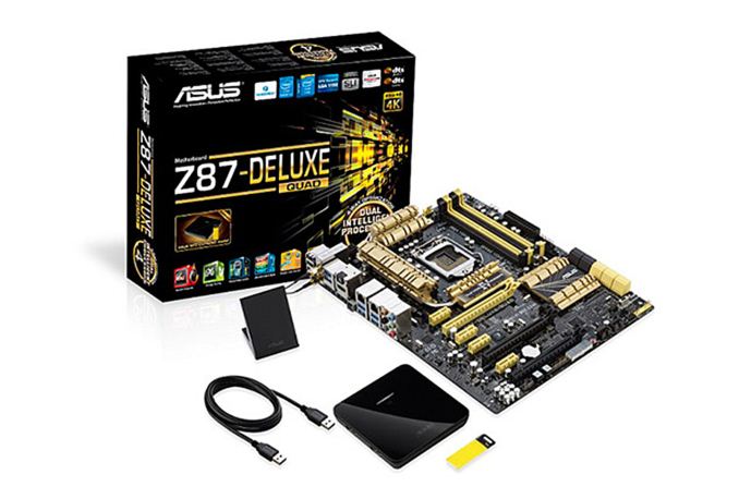
For those that need high bandwidth access to external devices, however, even 10Gb/s may not be enough—specifically, 4K video resolutions can require around 15Gb/s. As we’ve previously discussed, with Thunderbolt 2 Intel is doubling the bandwidth with Thunderbolt 2 up to 20Gb/s per port by combining the four 10Gb/s channels into two 20Gb/s channels, thus enabling support for 4K/60 support. The ASUS Z87-Deluxe/Quad motherboard is the first motherboard to support the standard, and as expected you get two 20Gb/s ports courtesy of the single Falcon Ridge controller. Combined with the HDMI port, that gives the board the potential to drive three 4K displays at once. And if Thunderbolt 2 support isn’t enough for your enthusiast heart, ASUS is also including their NFC Express accessory for Near-Field Communication.
Here’s the short specifications summary for the Z87-Deluxe/Quad; we’re awaiting further details on expected availability and pricing, but given the Z87-Deluxe/Dual runs $350 we’d expect the new board to come in above that price point.
- 2 x Intel Thunderbolt 2 ports
- 1 x HDMI port
- 4 x DIMM slots
- 3 x PCIe 3.0/2.0 x16 slots
- 10 x SATA 6Gbit/s ports
- 8 x USB 3.0 ports with USB 3.0 Boost
- 8 x USB 2.0 ports
- ATX form factor
More...
-
08-20-13, 05:30 AM #3236
Anandtech: Nixeus VUE 30: 30" 2560x1600 IPS Monitor Review
Over the past 18 months, we’ve all been happy to watch as the price of 27” 1440p monitors has steadily fallen. With cheaper import panels becoming available, the cost of moving up to a high resolution panel has fallen considerably. I reviewed the Nixeus VUE 27 last year as it was the cheapest way at the time to get a 1440p panel while still getting a US warranty. Now Nixeus is back with a 30” monitor, the Nixeus VUE 30. With the 16:10 aspect ratio that commenters continually ask for and an IPS panel, will this mark the shift of a downward trend for 30” monitor prices as well?
More...
-
08-20-13, 03:31 PM #3237
Anandtech: NVIDIA 326.80 Beta Drivers Available Splinter Cell: Blacklist Ready
NVIDIA is pretty good about staying on top of the latest releases with updated drivers, and today is no different. Building from the current 326.41 Beta release, today’s 326.80 release works with GeForce-to-SHIELD streaming and is also the recommended driver for the Windows 8.1 Preview. The only other noteworthy change mentioned in the release notes is that this is a Game Ready driver designed to offer the best gaming experience for Splinter Cell: Blacklist, which hits retail and online stores in North America today as well.
Reviews of the new title (at least on consoles) have been generally favorable, and it’s available for all the major platforms—PS3, Xbox 360, and Wii U, along with PC. Obviously you don’t need the new drivers for any of the consoles, and if it’s like other recent Ubisoft titles you’ll need to play it through Ubisoft’s Uplay service. (Cue the groaning.)
As usual, the drivers are available for all the modern platforms: Windows 7/8/8.1 for desktops and laptops, and desktops also get XP and Vista drivers. I won’t bother linking the XP desktop drivers, since I don’t personally know anyone running NVIDIA Kepler GPUs with XP these days, but if you happen to fall into that camp you can find them at the usual place.
Windows Vista/7/8 64-bit Desktop
Windows Vista/7/8 32-bit Desktop
Windows 7/8 64-bit Mobile
Windows 7/8 32-bit Mobile
More...
-
08-20-13, 08:30 PM #3238
Anandtech: Intel Talks about Multimode LTE Modems - XMM7160 and Beyond
Since acquiring Infineon and forming the Mobile Communications Group, Intel has been relatively quiet about its modem portfolio and roadmap. Pre-acquisition parts from Infineon have continued to see broad adoption in the 2G (Nokia Aisha phones) and 3G market, like XMM6260 and XMM6360 which was in the international version of the Galaxy S 4. However, Intel has been relatively silent about its multimode LTE offering, XMM7160, since talking about it MWC.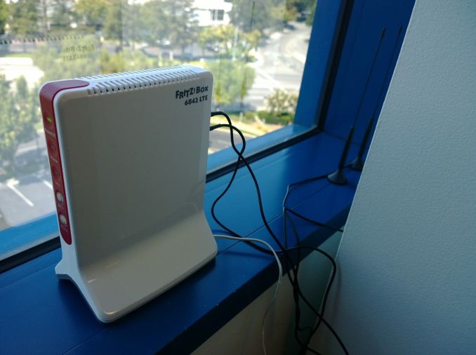
Yesterday Intel invited me and a few other press and analysts out to its Santa Clara office to talk about its modem portfolio, roadmap, and the future of its LTE products. The timing of the event was interesting since the Galaxy Tab 3 10.1 will be the first tier–1 product to launch with Intel’s XMM7160 LTE modem inside, although Intel has been quick to point out that XMM7160 was used in a single mode LTE manner in another prior device. The other part of it is Intel’s shift in approach which puts the mobile comms group in a much better position relative to the core business. Mobile players are going to have to be much louder about their modem roadmaps and integration strategies in this brave new mobile world, and Intel is going to start being much more open about what mobile comms is working on. The silence which made Intel’s wireless plays seem rather mysterious have now given way to a much more open dialog about what’s coming.
So first up is Intel’s XMM7160 multimode 2G (GSM/EDGE), 3G (HSPA+) and 4G (LTE) modem, which is shipping this August in the Galaxy Tab 3 10.1 and apparently a few other devices. I don’t expect this to show up in many phones, but obviously tablets and other devices built on Intel’s SoC platforms are obvious places. This is Intel’s first multimode LTE modem, and is a UE Category 3 part at launch (100 Mbps downstream) but will receive an upgrade to Category 4 (150 Mbps) via a firmware update in the December timeframe. There’s no silicon respin or increase in clocks, it’s just a software update after the Category 4 version passes certification. Infineon did a similar software upgrade with XMM6160 that enabled 64QAM (HSDPA 21.1) a while ago, the upgrade for XMM7160 is essentially analogous. The modem is also DC-HSPA+ compatible (42 Mbps) and is voice enabled for both VoLTE with the full IMS stack running on the modem and the more traditional CS fallback approach. XMM7160 is still built on TSMC’s 40nm CMOS process, and its SMARTi 4G transceiver is built on 65nm at TSMC, but Intel still claims it has a 20–30% power advantage for modem and RF compared to a competitor smartphone platform, though it wouldn’t say which.
Power claims aside, the real highlight of XMM7160 is the number of ports on its transceiver, which enables up to 15 LTE bands per device. That’s 15 ports primary receive, diversity receive, and transmit. Intel’s single PA approach carries on with XMM7160 as well which they claim leads to less area dedicated to the RF frontend and less total integration area (around 400 square mm) compared to competitors, even if the baseband and transceiver packages themselves are bigger. I asked for the high/mid/low port breakdown for SMARTi 4G but Intel wasn’t ready to disclose those details. XMM7160 has allegedly passed certification with all the tier one operators for North America, Europe, and Asia.
Intel showed off a demo of XMM7160 doing category 3 speeds attached to a base station emulator, 100 Mbps down and 50 Mbps up, without any stuttering, and completing a loopback VoLTE call. In addition they had a Fritzbox 6842 which includes XMM7160 attached to AT&T’s LTE network and let us run tests over the network. I saw speeds on par with what I was getting with the Moto X on AT&T which is based on Qualcomm's MDM9x15 IP block in MSM8960Pro. As an aside, it's hilariously ironic seeing 100 Mbps demos and then getting sub 10 Mbps on AT&T's live and increasingly loaded LTE network in Santa Clara, CA.
Intel also gave us a preview and a few details about its 2nd generation LTE multimode modem, XMM7260. This moves to a 28nm process at TSMC, Intel wouldn’t say however if it was LP, HPM or HPL. XMM7260 is planned to be Category 6 compatible (300 Mbps) and include carrier aggregation support through the next revision of transceiver, which also moves to 28nm CMOS. Intel showed a brief demo with an early revision of XMM7260 doing single spatial stream 10+10 MHz aggregation of bands 17 and 4 on a base station emulator. The next revision transceiver will allegedly also add 5 to 6 ports, bringing the total up to between 20 and 21 bands of LTE.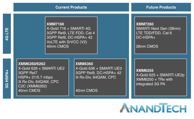
The only remaining question is TDD support for both TDD-LTE and TD-SCDMA. Intel hasn’t decided whether to launch TDD support on XMM7160 which is capable of supporting it via a discrete coprocessor, or just waiting for 7260.
Intel knows it’s late to LTE and is still transitioning the Infineon assets from a fast follower model to a position of leadership. By its own admission this adaptation is still not over, but the schedule for XMM7260 looks very ambitious (just 9 months between XMM7160 and XMM7260, putting it in the first half of 2014), and inclusion of Cat 6 support would put it considerably closer if not ahead of Qualcomm’s unannounced MDM9x25 successor. The transition of modem to Intel Architecture (away from two different DSP architectures) also remains to be seen, and I'm told it will be two to three years before Intel's modems are ready to intercept the Intel fabrication roadmap and get built on Intel silicon instead of at TSMC. Either way I’m glad Intel Mobile Comms is being much louder about its modem strategy.
Gallery: Intel Talks about Multimode LTE Modems - XMM7160 and Beyond


More...
-
08-21-13, 02:00 AM #3239
Anandtech: Samsungs V-NAND: Hitting the Reset Button on NAND Scaling
SSD pricing has come down tremendously since Intel’s X25-M hit the scene in 2008. Back then we were talking about 80GB for around $600, while today Micron and Samsung will sell you a 1TB SSD for the same price. Moore’s Law drove this scaling in capacity. Smaller transistors paved the way for higher density NAND in the same die area, and increasing volumes helped to keep the fabs full.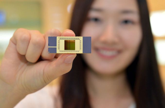
Although scaling transistor size helped address the cost-per-bit problem, it created a new one: decreasing endurance and performance. Just looking at what’s happened to IMFT NAND over the past few generations gives us an idea of what we’re dealing with:
Both endurance and performance trend downwards. Modern SSDs deal with the endurance problem by implementing sophisticated error checking/correction, and the performance problem is masked by exploiting parallelism as best as possible.Micron NAND Evolution 50nm 34nm 25nm 20nm 20nm 16nm Program Page (typical) 900 µs 1200 µs 1300 µs 1300 µs 1600 µs ? Rated Program/Erase Cycles 10000 5000 3000 3000 3000 ~3000
The root cause is basic physics. To store 2 bits per cell in present day MLC NAND, we’re talking about counting a couple dozen electrons. Go to 3 bits per cell (TLC NAND) and the difference between levels shrinks further. Scale down to 14/15/16nm NAND and everything gets more difficult. We’re heading towards a situation where the difference between levels in a NAND cell are a matter of a handful of electrons.

Measuring such subtle differences in stored charge is difficult, especially when NAND cells continue to shrink and are packed very tightly together. Interference between the cells becomes a much bigger concern below 20nm. Back at 50nm these sorts of issues were easy to mitigate with decent controllers and good quality NAND. Now we’re seeing more sophisticated ECC and DSP-like work being done by the controller in order to get accurate data in/out of the drive.
Scaling of traditional NAND via smaller manufacturing processes will come to an end. I’ve heard estimates saying we’ll see one or two more shrinks before it becomes unfeasible to scale cell size any further. The question then becomes: what’s next?
Last week Samsung gave their answer: V-NAND, a 3D NAND leveraging charge trap flash technology.
How it Works
Rather than increasing density by shrinking cell size, Samsung’s V-NAND takes a few steps back in process technology and instead stacks multiple layers of NAND cells on top of one another.

The change isn’t so simple. I’ve used the floating gate transistor diagram in many of our big SSD articles in the past, but that cell design doesn’t apply to V-NAND. In the floating gate MOSFET, electrons are stored on the gate itself - a conductor. Defects in the transistor (e.g. from repeated writes) can cause a short between the gate and channel, depleting any stored charge in the gate. If the gate is no longer able to reliably store a charge, then the cell is bad and can no longer be written to. Ultimately this is what happens when you wear out an SSD.
With V-NAND, Samsung abandons the floating gate MOSFET and instead turns to its own Charge Trap Flash (CTF) design. An individual cell looks quite similar, but charge is stored on an insulating layer instead of a conductor. This seemingly small change comes with a bunch of benefits, including higher endurance and a reduction in overall cell size. That’s just part of the story though.
V-NAND takes this CTF architecture, and reorganizes it into a non-planar design. The insulator surrounds the channel, and the control gate surrounds it. The 3D/non-planar design increases the physical area that can hold a charge, which in turn improves performance and endurance.
The final piece of the V-NAND puzzle is to stack multiple layers of these 3D CTF NAND cells. Since Samsung is building density vertically, there’s not as much pressure to shrink transistor sizes. With relaxed planar space constraints, Samsung turned to an older manufacturing process (30nm class, so somewhere between 30 and 39nm) as the basis of V-NAND.
By going with an older process, Samsung inherently benefits from higher endurance and interference between cells is less of an issue. Combine those benefits with the inherent endurance advantages of CTF and you end up with a very reliable solution. Whereas present day 19/20nm 2-bit-per-cell MLC NAND is good for around 3000 program/erase cycles, Samsung’s 30nm-class V-NAND could withstand over 10x that (35K p/e cycles).
The move to an older process node doesn’t even come at a reduction in density thanks to just how high Samsung can stack its V-NAND. In its announcement last week, Samsung introduced a first generation 128Gbit MLC V-NAND solution with 24 layers. The 128Gbit device delivers 2x the density in the same physical space as a 19/20nm 64Gbit device, or roughly equivalent density to a traditional 128Gbit planar device at 15nm - the obvious benefit being better endurance, and performance.
Since we’re dealing with physically larger NAND cells that are also less susceptible to certain types of interference, program times are lower - meaning that performance is higher. With fewer retries required for all reads/writes, overall power consumption can be lower as well. At the end of the day, it’s just a better solution.

Samsung went one step further and announced that it was sampling an enterprise SSD built around V-NAND to key customers. Since V-NAND is presently only available in a 128Gbit density, capacities aren't anything earth shattering but I suspect that'll change soon enough. It’s too early to talk about pricing and availability unfortunately.

V-NAND is the future for Samsung. We’ll see V-NAND in appear in enterprise, client and even mobile (phones/tablets). There will likely be a period of overlap as Samsung transitions to V-NAND, but expect to see that transition begin next year across multiple markets.

A 128Gbit device is nice, but that’s not the end of the road. Samsung is predicting it’ll be able to build a 1Tb device by 2017, showcasing just how much scaling it can get out of 3D NAND. Samsung could theoretically also move to a smaller process node to further increase density, although ultimately that will run into the same limitations we’re facing today with traditional, planar NAND. The initial design only stores two bits per cell, but if need be Samsung could also move to a TLC V-NAND.
What about the rest of the present day NAND players? I suspect those that don’t move to CTF and/or 3D NAND will instead have their sights set on a bigger departure from NAND: some form of resistive RAM. The potential performance gains there are even higher, and you can also deploy a vertically stacked solution to gain density.
The good news is that it looks like we’re going to have some great options that will enable continued improvements in SSD density, cost and performance.
More...
-
08-21-13, 09:31 AM #3240
Anandtech: GIGABYTE F2A85XN-WiFi Review: FM2 and Richland in mini-ITX
Mini-ITX is an exciting form factor, as with every CPU generation we can make something small and faster with better features over the previous gen. GIGABYTE recently released a mini-ITX motherboard for AMD APUs, and we have it in to test – the F2A85XN-WiFi.
More...


 Quote
QuoteThread Information
Users Browsing this Thread
There are currently 57 users browsing this thread. (0 members and 57 guests)


Bookmarks