

Results 4,481 to 4,490 of 12096
Thread: Anandtech News
-
11-11-14, 12:01 PM #4481
Anandtech: Intel Launches M.2 and Larger Capacity 2.5" SSD DC S3500 Models
Two years ago Intel released the DC S3500 and S3700 SSDs that marked as the company's first truly in-house SATA 6Gbps SSDs. Today Intel is adding M.2 form factor to the S3500 lineup along with higher capacity options in the regular 2.5" size.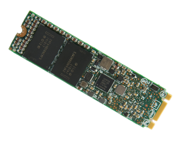
The original S3500 came in capacities ranging from as small as 80GB to up to 800GB, but with the increasing demand for high density storage, Intel is adding 1.2TB and 1.6TB offerings. There is no change in the Flash Translation Layer (FTL) design to accommadate the extra NAND nor are there any other firmware or hardware changes, so the new models simply have more NAND on the board.
The 1.2TB and 1.6TB models provide higher randon write speeds, which makes sense given the additional NAND. Typically steady-state random write performance increases with more NAND thanks to increased parallelism, although only to a certain threshold since more NAND also adds tracking overhead. In the case of the S3500, the 1.2TB model appears to be the sweetspot by offering 18.5K random write IOPS, whereas the 1.6TB SKU drops that figure to 14.6K IOPS. Moreover, write endurance scales nearly linearly with the capacity as the 1.2TB is rated at 660TB and the 1.6TB at 880TB, while the existing 600GB and 800GB models are rated at 330TB and 450TB respectively.
The M.2 version of the S3500 is one of the first enterprise-class SSDs in M.2 form factor. Feature wise the M.2 models are equal to their 2.5" counterparts, meaning that there is full power-loss protection, end-to-end data protection and AES-256 encryption. The M.2 models come in M.2 2280 form factor and due to the space constraints, only 80GB, 120GB and 340GB capacities are available.
The M.2 models actually carry slightly higher random write speeds compared to their 2.5" counterparts, although that comes at the slight expense of random read performance. Since there is no metal chassis to help with heat dissipation, the M.2 models are a bit more exposed to thermal throttling, although Intel assured that as long as there is enough airflow in the system the drive should stay within its operating temperatures and not throttle itself.
At this stage M.2 hasn't really been adopted by the enterprise space yet, but there is a growing interest for it due to the space savings. Intel told me that they are in talks with multiple OEMs about integrating the M.2 S3500 to servers, but as of now the main market for the S3500 is embedded devices. This includes devices like ATMs, slot machines and cash registers, which are transitioning to SSDs to save space and increase reliability. The S3500 is certainly a good fit for that segment with its enterprise-class feature set, whereas most M.2 drives on the market lack features like full power-loss protection.
While many consumer drives are selling at below $0.50/GB, the enterprise features and additional validation increase the cost of the S3500. At right below the $1 per GB mark, the S3500 is, however, a rather competitive drive in the entry-level enterprise segment.
More...
-
11-11-14, 03:00 PM #4482
Anandtech: NVIDIA VXGI Apollo 11 Demo Available
When NVIDIA held their press briefing on the upcoming GM204 Maxwell GPUs back in September, one of the big new features for Maxwell 2.0 was VXGI – Voxel Global Illumination. As part of the presentation, NVIDIA did their best to recreate the famous photo from the lunar landing that took place 45 years ago, and in the process they hoped to debunk some of the "inconsistencies" that conspiracy theorists have been going on about for decades.
Today, on 11/11, the Apollo 11 demo is now available to the public. Of course it's doubtful anyone that believes in the conspiracy theories will change their mind thanks to the NVIDIA demo, but it's at least a demonstration of VXGI that end users can run. Among other things, you can adjust camera exposure, sun position, and toggle Buzz Aldrin on/off (he had to be outside the lunar module to take the photo after all), all of which effect the scene rendering in real time.
Since the Apollo 11 demo uses VXGI, it does require NVIDIA's latest GM204 GPUs in order to run – Radeon and older GeForce users need not apply. I tested it with a GTX 970 and it ran "okay" (15~35 FPS, depending on the view), indicating as we suspected that you'll need a whole lot of GPU power if you want to do this level of VXGI in a real-time game. The demo also appears to be locked to a resolution of 1920x1080, or at least there's no feature to change the resolution within the demo itself (it appears hacking the binaries would be required, as there's no configuration file either). Considering the frame rates are already a bit low, however, trying to render VXGI at 2560x1440 would really require at least two GPUs to do it justice.
Below is a gallery of screenshots from the demo, and if nothing else it's a sign of things to come with global illumination. Real-time path tracing is still a long ways off for consumer hardware, but VXGI provides a better approximation of path tracing compared to existing algorithms and we could see the technology start showing up in games within the next year or two. The demo was built using Unreal Engine 4 as well, and Tim Sweeney has talked about voxel-based lighting in the past, which means there's a good chance VXGI support could end up widely adopted by UE4-based games. In the famous words of Captain Picard, "Make it so!"
Gallery: NVIDIA VXGI Apollo 11 Demo Available


More...
-
11-11-14, 04:33 PM #4483
Anandtech: AMD Catalyst 14.11.1 Beta Drivers Available
As we've noted in a few recent NVIDIA driver articles, there are a ton of new games coming out right now, which of course means we'll need to drivers/profiles in some cases to get optimal performance. Today AMD has released their beta Catalyst 14.11.1 drivers, with support for all recent AMD GPUs. Specifically, the new drivers support HD 7000 and newer desktop GPUs, and HD 7000M and newer Enduro notebooks – non-Enduro notebooks apparently are not supported. The actual display driver version is now at 14.301-141105a-177561E. Windows 7 or 8/8.1 are required as well.
In terms of updates, the Release Notes specifically call out performance improvements and CrossFire profile updates for Call of Duty: Advanced Warfare and Assassin's Creed: Unity; the latter just launched this morning (at midnight) while Call of Duty was released last week. The performance improvements apply to both single GPUs and CrossFire configurations, though the only figures we have right now are that Call of Duty has "up to 30% performance increases with FXAA and lower game resolutions". If you're currently playing either game on an AMD GPU, give the drivers a shot and let us know in the comments how it goes.
More...
-
11-11-14, 07:01 PM #4484
Anandtech: Samsung Files Counter-Suit & Patent Infringement Claims Against NVIDIA & V
Back in September NVIDIA filed patent infringement complaints against Samsung and Qualcomm. The crux of the issue being that NVIDIA believes that GPUs from Qualcomm, ARM, and Imagination all violate several of NVIDIA’s patents. Ultimately after failing to come to a licensing agreement with Samsung, NVIDIA took the matter to the courts. Complicating the matter is that in the case of infringement there is uncertainly and disagreement over who would be responsible – the chip designer or the hardware vendor – which led to NVIDIA taking the especially risky step of filing the suit against both Samsung and one of their GPU suppliers, Qualcomm.
This is a case that will take years to resolve, but in the meantime given the high profile nature of the case and the powerful parties involved, there was a high probability that counter-suits would be filed in response to NVIDIA’s initial complaints. This came to pass last week, with Samsung filing a suit in US federal court accusing NVIDIA and system builder Velocity Micro of infringing on multiple Samsung patents and false advertising regarding the SHIELD Tablet (to the detriment of Samsung).
Overall Samsung’s patent claims involve 8 patents, with NVIDIA accused of violating 6 and Velocity Micro accused of violating all 8. Interestingly, the patents range from technical (cache control) to physical (“method for rolling a metal strip”), which is why NVIDIA is not being accused of violating all 8 patents since they are a fabless semiconductor firm. The inclusion of Velocity Micro in turn is rather odd at first, and this appears to be a case of Samsung going after both the IP designer and the hardware vendor just as NVIDIA did with their initial suit against Samsung and Qualcomm. Velocity Micro in turn is one of NVIDIA’s closest partners, and they are involved in selling selling systems containing the full triad of NVIDIA products: GeForce, Quadro, and Tesla.
Like NVIDIA’s initial suit it will likely take years to resolve Samsung’s suit if it goes all the way. More likely however this is a calculated move on Samsung’s part for if the two firms reach a negotiated settlement. By counter-suing NVIDIA over patent infringement, Samsung has the option to take NVIDIA to the bargaining table and cross-license patents as opposed to paying licensing fees, a significantly cheaper outcome to say the least. However all of this is contingent on which patent infringement claims are upheld and whether the two firms let their respective cases even go that far, as the two can always settle beforehand.
In the meantime this is likely not the last we have heard of this case. With the expected court date still years off and the US International Trade Commission conducting their own investigation, there is a lot left to happen before any of these suits reach a courtroom.
More...
-
11-11-14, 10:30 PM #4485
Anandtech: Apple A8Xs GPU - GXA6850, Even Better Than I Thought
Working on analyzing various Apple SoCs over the years has become a process of delightful frustrating. Apple’s SoC development is consistently on the cutting edge, so it’s always great to see something new, but Apple has also developed a love for curveballs. Coupled with their infamous secrecy and general lack of willingness to talk about the fine technical details of some of their products, it’s easy to see how well Apple’s SoCs perform but it is a lot harder to figure out why this is.
Since publishing our initial iPad Air 2 review last week, a few new pieces of information have come in that have changed our perspective on Apple’s latest SoC. As it turns out I was wrong. Powered by what we’re going to call the GXA6850, the A8X’s GPU is even better than I thought.
Briefly, without a public die shot of A8X we have been left to wander through the dark a bit more than usual on its composition. A8X’s three “Enhanced Cyclone” CPU cores and 2MB of L2 cache were easy enough to discover, as the OS will cheerfully report those facts. However the GPU is more of an enigma since the OS does not report the GPU configuration and performance is a multi-variable equation that is reliant on both GPU clockspeed and GPU width (the number of clusters). Given Apple’s performance claims and our own benchmarks we believed we had sufficient information to identify this as Imagination’s PowerVR GX6650, the largest of Imagination’s GPU designs.Apple SoC Comparison A8X A8 A7 A6X CPU 3x "Enhanced Cyclone" 2x "Enhanced Cyclone" 2x Cyclone 2x Swift CPU Clockspeed 1.5GHz 1.4GHz 1.4GHz (iPad) 1.3GHz GPU Apple/PVR GXA6850 PVR GX6450 PVR G6430 PVR SGX554 MP4 RAM 2GB 1GB 1GB 1GB Memory Bus Width 128-bit 64-bit 64-bit 128-bit Memory Bandwidth 25.6GB/sec 12.8GB/sec 12.8GB/sec 17.1GB/sec L2 Cache 2MB 1MB 1MB 1MB L3 Cache 4MB 4MB 4MB N/A Transistor Count ~3B ~2B >1B N/A Manufacturing Process TSMC(?) 20nm TSMC 20nm Samsung 28nm Samsung 32nm
Since then, we have learned a few things that have led us to reevaluate our findings and discover that A8X’s GPU is even more powerful than GX6650. First and foremost, on Monday Imagination announced the PowerVR Series7 GPUs. Though not shipping for another year, we learned from Imagination’s announcement that Series7XT scales up to 16 clusters, twice the number of clusters as Series6XT. This immediately raises a red flag since Imagination never released an 8 cluster design – and indeed is why we believed it was GX6650 in the first place – warranting further investigation. This revelation meant that an 8 cluster design was possible, though by no means assured.
The second piece of information came from analyzing GFXBench 3.0 data to look for further evidence. While we don’t publish every single GFXBench subtest in our reviews, we still collect the data for Bench and for internal use. What we noticed is that the GFXBench fill rate test is showing more than double the performance of the A8 iPhone 6 Plus. Keeping in mind that performance here is a combination of width and clockspeed, fillrate alone does not prove an 8 cluster design or a 6 cluster design, only that the combination of width and clockspeeds leads to a certain level of performance. In other words, we couldn’t rule out a higher clocked GX6650.
PowerVR Series7XT: Up 16 Clusters, Twice As Many As Series6XT
At the same time in the PC space the closest equivalent fillrate test, 3DMark Vantage’s pixel fill test, is known to be constrained by memory bandwidth as much as or more than it is GPU performance (this leading to the GTX 980’s incredible fillrate). However as we have theorized and since checked with other sources, GFXBench 3.0’s fillrate test is not bandwidth limited in the same way, at least not on Apple’s most recent SoCs. Quite possibly due to the 4MB of SRAM that is A7/A8/A8X’s L3 cache, this is a relatively “pure” test of pixel fillrate, meaning we can safely rule out any other effects.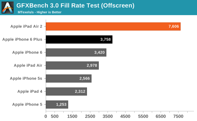
With this in mind, normally Apple has a strong preference for wide-and-slow architectures in their GPUs. High clockspeeds require higher voltages, so going wide and staying with lower clockspeeds allows Apple to conserve power at the cost of some die space. This is the basic principle behind Cyclone and it has been the principle in Apple’s GPU choices as well. Given this, one could reasonably argue that A8X was using an 8 cluster design, but even with this data we were not entirely sure.
The final piece of the puzzle came in this afternoon when after some additional poking around we were provided with a low resolution (but still good enough) die shot of A8X. Unfortunately at this point we have to stop and clarify that as part of our agreement with our source we are not allowed to publish this die shot. The die shot itself is legitimate, coming from a source capable of providing such die shots, however they didn’t wish to become involved in the analysis of the A8X and as a result we were only allowed to see it so long as we didn’t publish it.
With that said, while we can’t publish an image we can describe the die shot in full. To get right down to business then, the die shot confirms what we had begun suspecting: that A8X has an 8 cluster Series6XT configuration. All 8 GPU clusters are clearly visible, and perhaps unsurprisingly it looks a lot like the GPU layout of the GX6450. To put it in words, imagine A8’s GX6450 with another GX6450 placed right above it, and that would be the A8X’s 8 cluster GPU.
Or to put words into images, while we cannot publish the real die shot we have done the next best thing and created a rough A8X mock-up based on the excellent A8 die shot from Chipworks. This offers a quick overview of how A8X’s critical GPU and CPU components are organized.
With 8 clearly visible GPU clusters, there is no question at this point that A8X is not using a GX6650, but rather something more. And this is perhaps where the most interesting point comes up, due to the fact that Imagination does not have an official 8 cluster Series6XT GPU design. While Apple licenses PowerVR GPU cores, not unlike their ARM IP license they are free to modify the Imagination designs to fit their needs, resulting in an unusual semi-custom aspect to their designs (and explaining what Apple has been doing with so many GPU engineers over the last couple of years). In this case it appears that Apple has taken the GX6450 design and created a new design from it, culminating in an 8 cluster Series6XT design. Officially this design has no public designation – while it’s based on an Imagination design it is not an official Imagination design, and of course Apple doesn’t reveal codenames – but for the sake of simplicity we are calling it the GXA6850.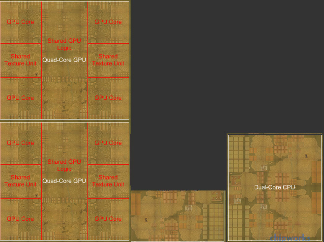
A8X Mock-Up From Chipworks' A8 Die Shot
Other than essentially doubling up on GX6450s, the GXA6850 appears to be unchanged from the design we saw in the A8. Apple did the necessary interconnect work to make an 8 cluster design functional and made their own power/design optimizations throughout the core, but there do not appear to be any further surprises in this GPU design. So what we have is an Apple variant on a Series6XT design, but something that is clearly a semi-custom Series6XT design and not a full in-house custom GPU design.Imagination/Apple PowerVR Series6XT GPU Comparison GXA6850 GX6650 GX6450 GX6250 Clusters 8 6 4 2 FP32 ALUs 256 192 128 64 FP32 FLOPs/Clock 512 384 256 128 FP16 FLOPs/Clock 1024 768 512 256 Pixels/Clock (ROPs) 16 12 8 4 Texels/Clock 16 12 8 4 OpenGL ES 3.1 3.1 3.1 3.1
Meanwhile the die shot places the die size of A8X at roughly 12.5mm x 10.0mm, or 125mm2. This is roughly in-line with our estimates – though certainly on the lower end – making A8X only a hair larger than the 123mm2 A6X. At roughly 3 billion transistors Apple has been able to increase their transistor count by nearly 50% while increasing the die size by only 40%, meaning Apple achieved better than linear scaling and A8X packs a higher average transistor density. On a size basis, A8X is a bit bigger than NVIDIA’s 118mm2 GK107 GPU or a bit smaller than Intel’s 2C+GT2 Haswell CPU, which measures in at 130mm2. Meanwhile on a transistor basis, as expected the 20nm A8X packs a far larger number of transistors than those 28nm/22nm products, with 3B transistors being larger than even Intel’s 4C+GT3 Haswell design (1.7B transistors) and right in between NVIDIA’s GK104 (3.5B) and GK106 (2.5B) GPUs.
Unofficial GXA6850 Logical Diagram
Of this die space GXA6850 occupies 30% of A8X’s die, putting the GPU size at roughly 38mm2. This isn’t sufficient to infer the GPU transistor count, but in terms of absolute die size it’s still actually quite small thanks to the 20nm process. Roughly speaking an Intel Haswell GT2 GPU is 87mm2, but of course Apple has better density.Apple iPad SoC Evolution Die Size Transistors Process A5 122mm2 1B 28nm A8X 125mm2 ~3B 20nm
Moving on, the bigger question at this point remains why Apple went with an 8 cluster GPU over a 6 cluster GPU. From a performance standpoint is greatly appreciated, but comparing iPad Air 2 to iPhone 6 Plus, the iPad Air 2 is nowhere near twice as many pixels as the iPhone 6 Plus. So the iPad Air 2 is “overweight” on GPU performance on a per-pixel basis versus its closest phone counterpart, offering roughly 30% better performance per pixel. Apple certainly has gaming ambitions with the iPad Air 2, and this will certainly help with that. But I believe there may also be a technical reason for such a large die.
The 128bit DDR3 memory bus used by the A8X requires pins, quite a lot in fact. Coupled with all of the other pins that need to come off of the SoC – NAND, display, audio, USB, WiFi, etc – and this is a lot of pins in a not very large area of space. At this point I am increasingly suspicious that Apple is pad limited, and that in order to fit a 128bit memory interface A8X needs to reach a minimum die size. With only a small organic substrate to help spread out pads, Apple has only as many pads as they can fit on the die, making a larger die a potential necessity. Ultimately if this were the case, Apple would have some nearly-free die space to spend on additional features if a 6 cluster A8X came in at under 125mm2, making the addition of 2 more clusters (~10mm2) a reasonable choice in this situation.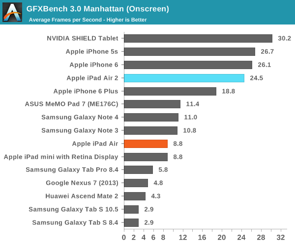
Finally, while we’re digging around in A8X’s internals, let’s quickly talk about the CPU block. There are no great surprises – nor did we expect to find any – but viewing the A8X die has confirmed that A8X is indeed an asymmetrical 3 CPU core design, and that there is no 4th (disabled) CPU core on the SoC. An odd number of CPU cores is unusual, though by no means unheard of. In this case Apple laid down a 3rd Enhanced Cyclone core, doubled the L2 cache, and left it at that.
Wrapping things up, it has become clear that with A8X Apple has once again thrown us a curveball. By drawing outside of the lines and building an 8 cluster GPU configuration where none previously existed, the A8X and its GXA6850 GPU are more powerful than even we first suspected. Apple traditionally aims high with its SoCs, but this ended up being higher still.
As far as performance is concerned this doesn’t change our initial conclusions – iPad Air 2 performs the same no matter how many GPU clusters we think are in it – but it helps to further explain iPad Air 2’s strong GPU performance. With 256 FP32 ALUs Apple has come very close to implementing a low-end desktop class GPU on a tablet SoC, and perhaps just as impressively can sustain that level of performance for hours. Though I don’t want to reduce this to a numbers war between A8X and NVIDIA’s TK1, it’s clear that these two SoCs stand apart from everything else in the tablet space.
More...
-
11-12-14, 07:30 AM #4486
Anandtech: Ingenic Launches Newton2: MIPS based IoT and Wearables Solution
The wearables and IoT market are moving very quickly, and only seven months after announcing their Newton platform, Ingenic is following up with Newton2. This pace reminds me of the glory days of consumer graphics cards, when NVIDIA and ATI were clawing for market share and would each produce two large launches per year. While the PC (and even smartphone) market has matured to a slower pace, the wearables and IoT market is currently quite frenetic. Dozens of companies worldwide are attempting to cash in on the explosive growth potential. Over time, we will see consolidation as contenders are crowned champions, but who those champions will be is anyone’s guess at the moment.
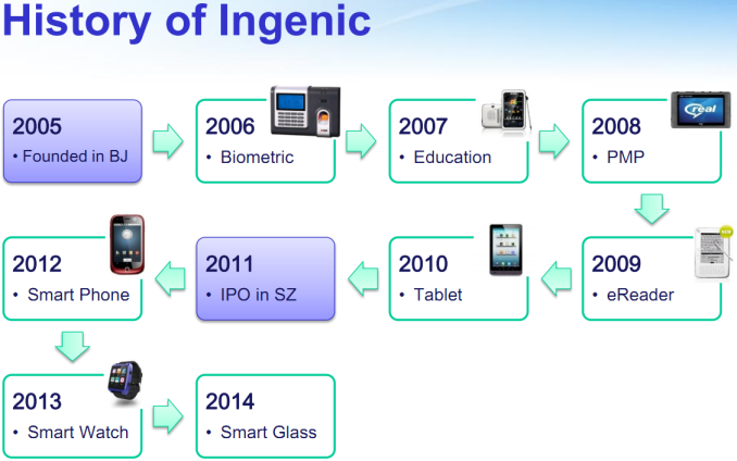
Ingenic is a relatively low profile company that could use an introduction. Ingenic is focused on semiconductors and devices and was founded in Beijing, China in 2005. Ingenic has licensed the MIPS architecture and designs their own CPU core and SoCs, and those designs are popular in low-end products such as digital picture frames, portable media players, and GPS devices. Ingenic had its IPO in 2011 and currently has a market cap of roughly $550 million.
Before getting to the details of Newton2, it’s important to understand positioning. Unlike other competitors, Ingenic positions the Newton (and Newton2) platform not as reference designs but instead as complete solutions. Ingenic would love to simply sell you the entire module as-is in high volume. However, Ingenic will build customized versions if you buy enough of them. This is similar to the Original Device Manufacturer (ODM) model, but in this case Newton is not an entire device but simply the electronics module. The purchaser still needs to place it into a full-fledged device like a smart watch or refrigerator. While Ingenic will sell you its custom designed SoCs as well, I am sure they would rather sell Newton as the margins for an integrated platform are guaranteed to be higher.
Now to the details. The Newton2 platform is a highly integrated module. These types of electronics are often referred to as a System on Module or SOM. Newton2 integrates the necessities of a wearable or IoT device, such as several built-in sensors and connectors for optional or obviously external components such as a display. Both Newton and Newton2 contain full featured application processors and can run Android.
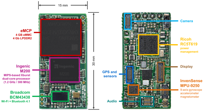
Power consumption for Newton is 4mW standby, 100mW average, and 260mW peak. Newton2 claims to cut standby consumption to 3mW.Ingenic Newton2 SOM Size 15mm x 30mm x 2.4mm SoC Ingenic M200 Memory 512MB LPDDR2 Storage 4GB eMMC WiFi Broadcom 43438 single-band 2.4GHz IEEE 802.11b/g/n PMIC Ricoh RC5T619 power management IC Bluetooth 4.1 Sensor IvenSense MPU-9250 gyroscope, accelerometer, magnetometer Interfaces Display, Capacitive Touch, DMIC and AOHPL/R Audio, MIPI-CSI or I2C Camera, UART, I2C, GPIO, RF 2.4 GHz antenna, USB 2.0 Software Android 4.4
The SoC on Newton2 is entirely new, the Ingenic M200. Notable inclusions in M200, beyond the bevy of traditional functionality, are the LCD and E-Ink display controllers, voice trigger processing offload, and the M200 SoC.
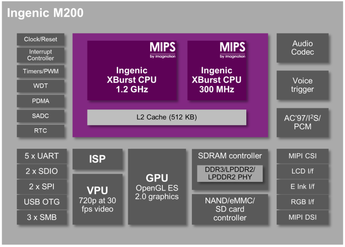
Keep in mind that not every M200 interface is exposed on the Newton2. For example, accessing all five UARTs would require integrating the M200 into your own custom board.Ingenic M200 SoC Package BGA270, 7.7mm x 8.9mm x 0.76mm, 0.4mm pitch CPU XBurst1-HP core, 1.2 GHz
XBurst1-LP core, 300 MHzGPU 2D/3D acceleration with OpenGL ES 2.0/1.1. OpenVG 1.1 VPU Video encoder up to 720p @ 30fps: H.264, VP8
Video decoder up to 720p @ 30fps: H.264, VP8, MPEG-1/2/4, VC-1, RV9ISP HDR, video and image stabilization, crop and rescale, auto exposure + gain + white balance + focus control, edge sharpening, noise reduction, color correction, contrast enhancement, gamma correction Memory DDR2, DDR3, LPDDR, LPDDR2 up to 667 Mbps
64-bit ECC NAND flash support Toggle 1.0 and ONFI2.0Display LCD controller with OSD: TFT, SLCD and MIPI-DSI (2-lanes)
E-Ink controllerCamera MIPI-CSI2 (2-lanes), DVP Audio Audio CODEC with 24-bit ADC/DAC, stereo line-in, MIC in, and headphone interface
Low power DMIC controller
AC97/I2S/SPDIF interface for external audio codec
One PCM interface, supports both master and slave modes
Voice trigger engine to wake system by programmable specific voiceADC 3 channels 12-bit SAR Interfaces USB 2.0 OTG x 1
MMC/SD/SDIO controller x 2
Full-duplex UART port x 5
Synchronous serial interface x 2
Two-wire SMB serial interface x 4Software Android 4.4
The CPUs inside the M200 SOC set this SOM apart. The M200 integrates two custom designed Ingenic XBurst1 processors using the MIPS32 Release 2 ISA and include floating point and SIMD. Each processor is a full applications processor (AP) with an MMU and caches. However, you can consider the M200’s CPUs heterogeneous as one CPU is performance optimized and operates at up to 1.2 GHz while the other is optimized for power consumption and runs at up to 300 MHz. This is something we have seen before from NVIDIA with their Tegra devices as well as ARM's big.LITTLE, but it's different than other wearable and IoT efforts where low power duties are handled by a simple microcontroller (MCU). Using two APs likely simplifies software development somewhat, even if they are different, as they aren’t as enormously different as an AP and an MCU.
Looking at the XBurst1 power consumption, these cores are significantly lower power than the Cortex-A5 which ARM specifies at 0.12 mW/MHz on the same 40nm LP process. Comparing these cores beyond their power consumption is outside the scope of this article, but it is worth pointing out because ARM is citing Cortex-A5 as their most power efficient wearable CPU.XBurst1 CPU Pipeline 9-stage, single issue Ingenic Estimated
Performance2.0 DMIPS/MHz ISA MIPS32 Release 2 (both Integer and Floating Point ISA)
XBurst SIMDMMU 32 dual-entry full associative joint TLB
4 entry ITLB
4 entry DTLBL1 Cache 32KB or 64KB I$ and D$ L2 Cache 256KB or 512KB Debug EJTAG Process 180nm, 90nm, 65nm, 40nm Ingenic Estimated
Power Consumption(1.0GHz, 0.09mW/MHz) @65nmLP
(1.2GHz, 0.07mW/MHz) @40nmLP, performance optimized
(500MHz, 0.05mW/MHz) @40nmLP, power optimized
The XBurst1 CPU core has been around since 2005, when Ingenic was founded. Ingenic revealed in 2013 it had purchased a MIPS64 license and was developing XBurst2 with design completion targeted at 2014. This will go hand in hand with Android 5.0 supporting MIPS64 ISA natively. Keeping with their roughly six month pace, it isn’t too farfetched to imagine a Newton3 platform sporting a MIPS64 XBurst2 with Android 5.0 launching in mid-2015.
More...
-
11-12-14, 12:30 PM #4487
Anandtech: The Nexus 6 Review
When consumers think of Google's Nexus devices, they think about the promise of receiving the latest updates for Android essentially as soon as they release. They also think about the value proposition that Nexus devices provide by giving good hardware at a price significantly lower than other smartphones. However, this was not always the case. The Nexus One, Nexus S, and Galaxy Nexus were all priced at the same level as other flagship smartphones. It was only with the launch of the Nexus 7 at $199 that we began to see a trend of inexpensive but still high quality devices coming from Google. That hasn't changed at all in the past few weeks. The Nexus 5 and Nexus 7 are both still available, and they still provide a very high quality experience, arguably better than some other smartphones that are both newer and more expensive. But Google's newest devices take aim directly at other flagship devices with both their specs and their prices. At $399 the Nexus 9 positions itself against Apple's iPad Mini 3, while the Nexus 6 at $649 goes up against essentially every other flagship smartphone. Read on for our full review of Google's Nexus 6.
More...
-
11-12-14, 01:32 PM #4488
Anandtech: Samsung Introduces Gear VR Innovator Edition for the U.S.
Today Samsung announced that their Gear VR Innovator Edition will be available in the United States starting in early December of this year. The Gear VR Innovator Edition is Samsung's head-mounted display that was developed in partnership with Oculus. Unlike the upcoming Oculus Rift, the Gear VR doesn't have an internal display. Instead, it acts like an accessory by using the Galaxy Note 4 as its display.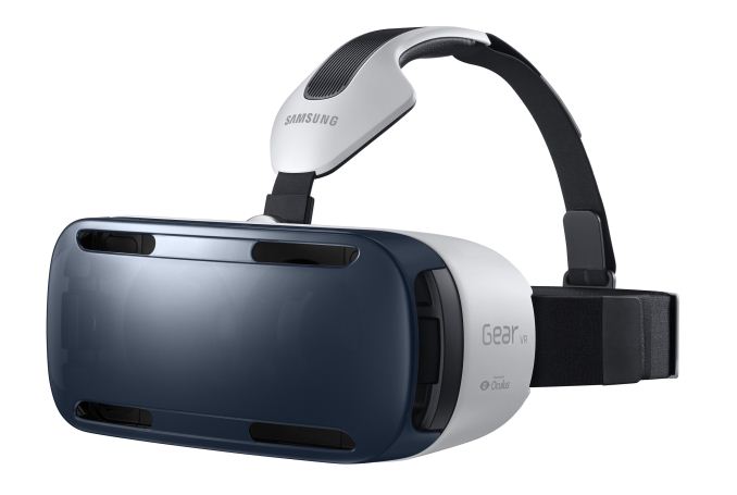
With the launch of the Gear VR Innovator Edition, Oculus will make its Oculus Mobile SDK for Gear VR available to developers. Samsung has also partnered with Oculus and other companies to make a variety of demos and services available for the Gear VR upon launch, which I've included in the list below.
- As part of the Marvel's Avengers: Age of Ultron partnership with Samsung, Gear VR users will gain exclusive access to Tony Stark's Lab inside the all new Avengers Tower.
- Cirque du Soleil Media presents a 360° live-action 3D VR experience, featuring an act from Zarkana filmed by Felix & Paul Studios.
- DreamWorks VR from DreamWorks Animation allows Samsung Gear VR users to interact and laugh with DreamWorks characters and content in a whole new way like never before.
- Harmonix Music VR takes your music library and transports you to a fully immersive, musically responsive environment, allowing you to relax in a vibrant soundscape and explore visualizations set to your favorite tracks.
- M-GO Advanced, a new paradigm for digital video VR applications, offers an unmatched interactive search and discovery experience with Samsung Gear VR.
- Oculus Home – Your VR home screen and content discovery center, which includes a Samsung section
- Oculus Store – An application that lets you browse and download new content from the Oculus platform
- Oculus Cinema – A VR movie theater and cinema where you can watch your favorite movies in an immersive virtual environment
- Oculus 360 Videos and Photos – Be immersed in 360° videos and panoramas like never before from within Gear VR
- Protocol Zero from DENA enables Samsung Gear VR players to infiltrate enemy grounds undetected in blackout conditions with hi-tech optics including night vision, X-ray vision, and thermal vision.
- Temple Run VR is the latest edition in Imangi’s Temple Run series, challenging Samsung Gear VR players to run as far as they can through a perilous winter wonderland as they escape the clutches of Arctic Demon Monkeys.
- Vevo offers more than 100,000 HD music videos, live concert events and original programming that can be enjoyed in an immersive, full-screen theater experience on Samsung Gear VR.
- WemoLab’s theBluVR allows users to immerse themselves in the dream-like majesty of marine life.
It certainly seems like Samsung has done a good job with making partnerships to provide content for the Gear VR. However, Samsung still hasn't given any firm details regarding pricing, which will definitely be a major part of what determines the success of the Gear VR. There have been rumors that it will be around $199, but Samsung is still not advertising an official price. Hopefully we'll get more details as the release date for the Gear VR Innovator Edition approaches. More details and some of the specifications for the Gear VR and the accompanying Galaxy Note 4 are available in the source below.
More...
-
11-12-14, 04:01 PM #4489
Anandtech: Benchmarked: Lords of the Fallen
Officially launched on October 28, Lords of the Fallen had a bit of a rocky start so it took longer for me to finish running benchmarks on the game, but I'll get into that momentarily. At its core, Lords of the Fallen is a melee third-person action-RPG similar in many ways to the Dark Souls games. There are periodic boss fights to shake things up, as you play the convicted criminal Harkyn (his face has tattoos to publicly declare his sins) trying to stop the invasion of the demonic Rhogar. The game has received decent reviews, with a current Metacritic score of 72%.
Like many recent releases, Lords of the Fallen is a multi-platform title that launched simultaneously for the PC, PS4, and Xbox One. The updated consoles now sport more memory than the old PS3 and Xbox 360, which gives developers opportunities to do a lot more in terms of textures and graphics quality, and at launch I think that ended up creating some problems on the PC. The short summary is that GPUs with 2GB of VRAM or less tended to have quite poor performance. CrossFire also had issues: it wasn't just functioning poorly but it actually caused the game to crash to the desktop.
The first update to the game was released about a week later, and it fixed a few bugs and instability issues, but more importantly it offered much better performance on GPUs with limited VRAM. CrossFire is also "working" now – and I put that in quotes because CrossFire is actually causing degraded performance in some cases and is basically not scaling well enough to be worth the hassle so far. Need I mention that this is an NVIDIA "The Way It's Meant To Be Played" title? Not that the developers have intentionally crippled AMD performance, but I don't think AMD has spent as much time optimizing their drivers for the game. It runs well enough with the right hardware and settings, but this is definitely a game that favors NVIDIA.
We tested using the game's built-in Ultra and High settings, but there's not a significant difference in performance or quality between the two modes so I'm in the process of running another set of performance figures at Medium quality. (I'm also testing Assassin's Creed: Unity performance, which will be the next Benchmarked article, so it will be a bit before I can post the full 1080p Medium results.) Before we get to the performance, here's a quick look at image quality using the four presets:
Gallery: Lords of the Fallen Graphics Quality Comparison-Ultra_thumb.jpg)
-High_thumb.jpg)
-Medium_thumb.jpg)
-Low_thumb.jpg)
-Ultra_thumb.jpg)
-High_thumb.jpg)
The major difference between Ultra and High seems to be a minor change in the handling of shadows; I'm not sure you could definitively call Ultra "better", and performance is so close that it's mostly a moot point. Medium appears to disable Ambient Occlusion on the shadows, resulting in a much more noticeable change to the graphics, while Low also disables the Post Processing effect. I'm not sure that's actually a bad thing, though – the effect warps the image a bit, particularly on the right and left thirds of the screen, and tends to make everything look a little blurry/weird.
Lords of the Fallen also features support for some NVIDIA technologies, including PhysX APEX particle support. Many of the effects use PhysX on the CPU and thus work with all GPUs (as well as running on the PS4 and Xbox One), but there's an additional effect called Turbulence that's only available on NVIDIA GPUs. I didn't try to do thorough testing of performance with and without Turbulence enabled since it's an NVIDIA exclusive, but informally it looks like the performance hit is relatively small – around 5-10% – so if you're running an NVIDIA GPU it's probably worth enabling.
One final thing to note before we get to the benchmarks is that Lords of the Fallen is very demanding when it comes to GPUs. Moderate hardware (e.g. Radeon R7 and similar, or NVIDA GTX 750 Ti and lower) are going to struggle to break 30FPS at 1080p Ultra or High settings, so 1080p Medium or even 1600x900 Medium might be required. I'll add the Medium results in the next day or two once I finish retesting. And once more as a quick overview, here's the hardware used for our Benchmarked articles:
Lords of the Fallen Average FPSGaming Benchmarks Test Systems CPU Intel Core i7-4770K (4x 3.5-3.9GHz, 8MB L3)
Overclocked to 4.1GHzMotherboard Gigabyte G1.Sniper M5 Z87 Memory 2x8GB Corsair Vengeance Pro DDR3-1866 CL9 GPUs Desktop GPUs:
Sapphire Radeon R9 280
Sapphire Radeon R9 280X
Gigabyte Radeon R9 290X
EVGA GeForce GTX 770
EVGA GeForce GTX 780
Zotac GeForce GTX 970
Reference GeForce GTX 980
Laptops:
GeForce GTX 980M (MSI GT72 Dominator Pro)
GeForce GTX 880M (MSI GT70 Dominator Pro)
GeForce GTX 870M (MSI GS60 Ghost 3K Pro)
GeForce GTX 860M (MSI GE60 Apache Pro)Storage Corsair Neutron GTX 480GB Power Supply Rosewill Capstone 1000M Case Corsair Obsidian 350D Operating System Windows 7 64-bit
As far as target FPS for a decent experience, Lords of the Fallen isn't quite as twitch-heavy as some games, so I'd recommend shooting for anything above 40FPS average. If you have a G-SYNC display with an NVIDIA GPU, that will also allow you to still experience "smooth" gameplay without tearing. For our testing, however, we disable VSYNC as usual.
Starting with average frame rates, 4K is basically a stretch at best for even the fastest single GPU configurations. The GTX 980 can technically break 30FPS (barely), but it's not as smooth as I'd like so dropping down a notch is recommended. SLI reportedly works well, though I don't have the hardware to test this (yet), so two high-end NVIDIA GPUs might be enough to get into the playable frame rate territory at 4K. At present CrossFire R9 290X still falls well short, but that's also due to the fact that CrossFire scaling is very low right now.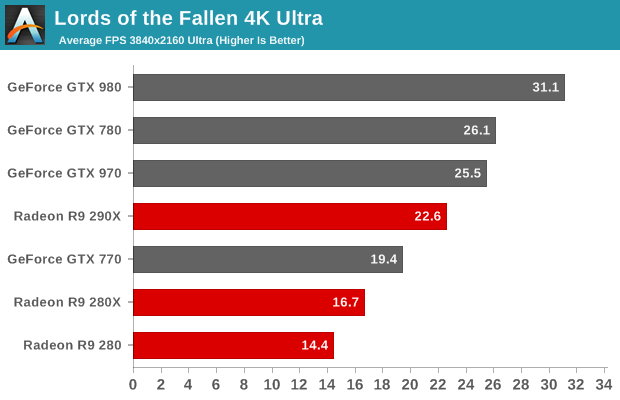
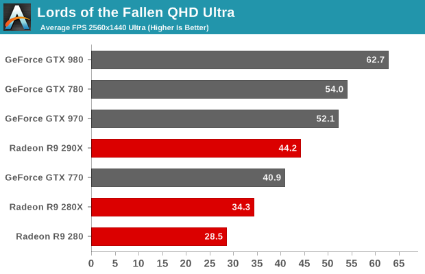
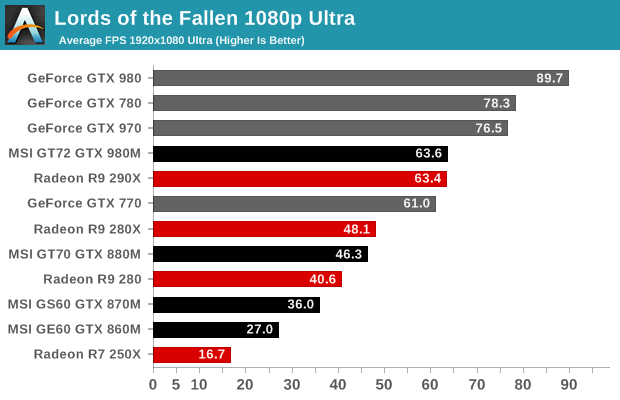
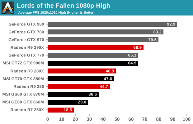
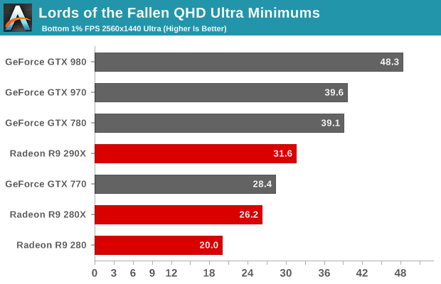
There's a sizeable jump in performance going from 4K to QHD as expected, with most of the GPUs basically doubling their performance – not too surprising as 4K has 2.25X as many pixels to render as QHD. I mentioned earlier how the patch changed performance in some cases, particularly for GPUs with 2GB or less VRAM. The big beneficiary for higher performance GPUs ends up being the GTX 770, which saw a jump in QHD performance of over 70% with the patch (and a still significant increase of 30% at 1080p Ultra/High).
On the AMD side of the equation, the R9 GPUs don't do all that well compared to NVIDIA. We're used to seeing the 780/970 trade blows with the 290X in most games, but here the 290X is closer to a 770, with the 780/970 offering a solid 15-20% increase in performance. Meanwhile the 280X is mostly playable at QHD but certainly not ideal, and the 280 has to drop to 1080p before it can achieve "acceptable" performance. Overall, the R9 290X along with all of the GTX desktop GPUs I tested can handle QHD Ultra and provide a good experience.
Moving to the 1080p results and looking at the laptops, the GTX 980M is clearly a force to be reckoned with, essentially matching the R9 290X and the GTX 770 and easily handling 1080p Ultra. The next step down to the GTX 880M is a pretty big one – the 980M is about 35% faster than the 880M – but the 880M is still able to handle 1080p Ultra. The 870M meanwhile is in that "questionable" range, and dropping to High settings is only good for about 3-5% more performance on most of our GPUs, so a bit more tweaking is going to be required. Last but not least, the 860M falls short of even the 30FPS mark, and it will need some tuning or Medium quality before it's really acceptable at 1080p.
Our sole "low-end" GPU is the R7 250X, and as you can see it's really not doing well at 1080p High, falling below 20FPS. It also benefited quite a bit from the patch, improving by around 35% at 1080p High, but going from 13.7 FPS to 18.5 FPS still means it's unplayable. I also tested an Intel HD 4600 just for fun (though it's not shown in the charts since it only managed 6.5 FPS); even at 1366x768 and Low quality, it's still far short of being playable with frame rates of around 17 FPS.
Lords of the Fallen Minimum FPS
As with Civilization: Beyond Earth, for the "minimum" FPS I'm actually using an average of the bottom 1% of frame rates. What that means is that this is a realistic look at minimum frame rates, as our benchmark run typically consists of a couple thousand frames of data so we're looking at an average of 20+ frames. Thus, a single frame that took a long time to render won't have as great of an impact as consistently low frame rates. The goal here is to give you a better idea of what performance will be like in the most graphically intense situations.
When we look at the minimum FPS, you can now see why I recommended at least 40FPS average frame rates for Lords of the Fallen to be "playable". That translates into minimum frame rates of roughly 30FPS, so even in higher complexity scenes the game will still stay reasonably smooth. On the other hand, if you're averaging closer to 30FPS, minimum FPS is going to drop into the low 20s, and that can be quite choppy.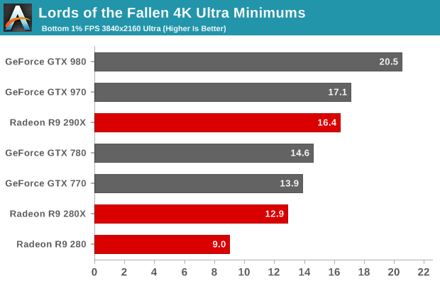
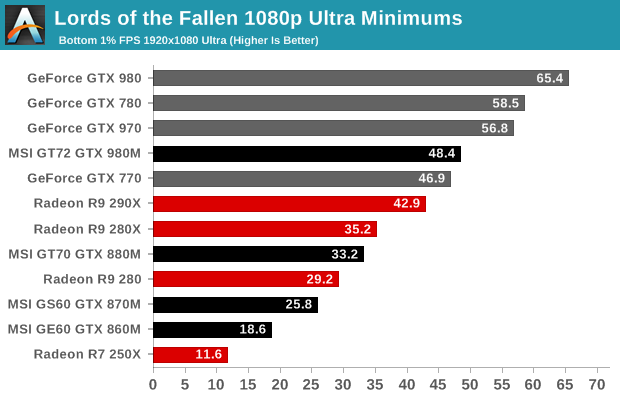
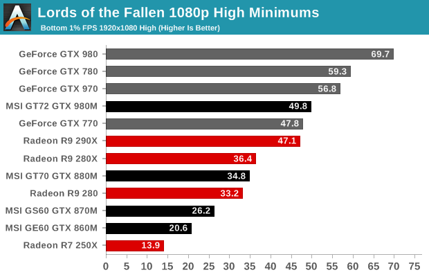
The standings of the various GPUs don't really change much in our minimum FPS results. In most cases the minimum is around 70-75% of the average FPS, with GPUs that have less RAM generally faring slightly worse than those with more RAM. NVIDIA seems to do a bit better than AMD at 1080p than at QHD, but there aren't any clear issues on any of the GPUs.
Closing Thoughts
I never played any of the Dark Souls games for whatever reason (lack of time, mostly), so for me Lords of the Fallen is actually pretty fun. Of course, having benchmarked the same sequence I don't know how many times (well over 100) does become rather tedious. With so many other games coming out right now, I don't think I'd place Lords of the Fallen at the top of any recommendations list, but it has enough to warrant picking it up if it goes on sale. In the meantime, I'd suggest Middle-Earth: Shadow of Mordor or Assassin's Creed: Unity as better games, at least in my opinion.
Now that we've had a few of these Benchmarked articles, let me also ask for reader feedback. The good thing about these Benchmarked articles is that once I'm done with the initial benchmarking, I won't necessarily be retesting this same game on different systems for another year or two. It's also useful to increase the number of games we benchmark, as it helps to keep the GPU manufacturers honest – they can't just optimize drivers for the ten or so games that most sites use for benchmarking as an example. But what do you think – do you like these articles? Short of the desire to test even more configurations (it's always something that would be nice to have but very time consuming to deliver), what else would you like to see? Are there any recently released games that you'd like to see us test? Let us know!
More...
-
11-12-14, 05:31 PM #4490
Anandtech: Windows 10 Technical Preview Gets Version Bump And New Features
Just three weeks ago, the Windows 10 Technical Preview got its first new build available to members of the Windows Insider program, and today we are seeing another version bump adding some new features and changes to the preview. As part of last month’s update, Microsoft enabled preview users to choose either the Fast or Slow lane for future updates. If you have selected Fast, you will be getting this build from Windows Update immediately, or if you do not want to wait you can go to Update and Recovery and check for a new build now. People who opted for the Slow release cycle can wait for the bugs to be worked out first.
There are just a couple of important changes with this go build, which is now 9879. The first involves the Task View and Search buttons on the task bar. Many people, especially those with limited task bar space, did not appreciate having two additional buttons on the task bar with no way to remove them, so with build 9879 there is now the option to remove one, or both. This was a feedback driven change, so it is minor, but nice to see them listening to feedback.
Another minor change which was just added last month was new animations for minimize and restore. Feedback on these animations was that they were too jarring, so they have been updated to be a bit less, well, animated.
As part of the removal of the Charms menu, app commands such as the Share charm and App settings was accessed through an ellipsis in the title bar, which many people found difficult to discover. The ellipsis has now been changed to the familiar hamburger menu button that has gained popularity in the mobile space, which should help with discoverability.
As for all new features, previewed last week at TechEd Europe were new trackpad gestures, and these are now available in the latest build:
- 3 finger up -> Task View
- 3 finger down -> Show Desktop
- 3 finger flick to left or right -> switches to previous app (go back 1)
- 3 finger move left or right -> Alt-Tab (Task View) pops up and you can select the app you want (remove fingers to select)
- 3 finger tap -> Search
As well, the new Snap Assist can now help when snapping apps across multiple monitors. As I just have Windows 10 in a VM, I can’t show a screenshot of this change other than the original snap assist shown here.
One of the bigger fundamental changes being introduced this month is a change to how OneDrive syncs on Windows 10. Users of Windows 8.1 will be aware of OneDrive using placeholders for files, and in File Explorer, it will say if the file is available offline or available online only. Any file you open would automatically download and stay synced on that PC unless you manually made it online only. This also worked with folders, allowing you to fairly easily specify if a folder should be synced to any particular PC. With OneDrive now offering unlimited storage, you can see that this is very important especially with the lowest cost devices coming with small amounts of usable storage. However Microsoft is saying that this confused people, because in File Explorer it would display files that were not on the device. Customers would then go somewhere with no connectivity assuming they had access to their files only to discover that they were set to online only. Starting with this build, OneDrive will now use selective sync, and the user can specify what they want synced. What you see in File Explorer will only be the files that are on that particular PC. Personally I really liked the placeholder approach from Windows 8.1, so I am disappointed in this change. For me, it was nice to see all of my files and easily download those I wanted to without having to go into any system menus. The files are clearly labeled as to whether they are available offline, so this is a bit of a shame. I will have to spend some time with the new method to see if I like it or not.
Another change to OneDrive is how to access it. In Windows 8.1, OneDrive was available as both a modern app, and an extension in File Explorer. This also caused some confusion apparently, since people would have multiple places to find their files. As a change for Windows 10, File Explorer will be the only way to access OneDrive files without using the web version I would assume. Although I understand Windows 10 is aimed at the desktop user, I am a bit confused as to what this means for the tablet user since using file explorer with Touch is fairly frustrating. Perhaps there will be a new touch based version of File Explorer presented when in Tablet mode.
Internet Explorer is getting some updates in this build as well, at least for some users. Ten percent of Insider participants will get the new Edge rendering engine available for them. To make it easy to offer direct feedback on this change, IE will have a emoticon in the upper right corner which a person can click to say that whatever site they are on is not rendering perfectly.
In the last build, MKV support was added, and in the new build they are completing this by having MKV files play directly in Windows Media Player and other desktop and modern apps. MKV will now display thumbnails and metadata in File Explorer, and DLNA/Play To support has been added. In addition, H.265 HEVC support has been added to the platform.
Finally, some rather minor changes have been made such as the ability to pin your favorite folders to Home, and a few new icons are inbound.
Just like the last build, this new build requires a re-provisioning of existing user accounts, so the install process is a bit longer than the normal patch/reboot that most people are accustomed to.
There are some good changes here, and some that I am not so sure about. Time with the build will be the only way to see if the changes work for me or not. If you are interested in trying out the Windows 10 Technical Preivew, check out http://preview.windows.com
Source: Windows Blog
More...


 Quote
QuoteThread Information
Users Browsing this Thread
There are currently 59 users browsing this thread. (0 members and 59 guests)


Bookmarks