

Results 4,491 to 4,500 of 12094
Thread: Anandtech News
-
11-12-14, 06:31 PM #4491
Anandtech: Motorola Begins Rollout of Android 5.0 Lollipop
Motorola has done a good job with keeping their devices updated. The fact that they don't ship dozens of different devices and use software that is close to what would be called stock Android certainly helps with this. Today Motorola has put up a posting on their blog which announces the beginning of their Android Lollipop rollout for their new Moto X and Moto G. Currently the update is rolling out in phases to the following three versions of those devices:
- Moto X (2nd Gen.) Pure Edition
- Moto G (2nd Gen.) US GSM
- Moto G (2nd Gen.) Global GSM retail versions sold in the US
The source for Lollipop was released only a week ago, and so this is a very good turnaround time from Motorola. There's no information about the original Moto X, Moto G, and Moto E, so we'll have to wait and see how those fit into Motorola's software support roadmap.
More...
-
11-13-14, 07:31 AM #4492
Anandtech: Windows 10 Technical Preview First Impressions: The Return Of The Desktop
Windows 10 is ditching the “One Interface to Rule them All” mentality, and moving to a more user friendly model of a single store across all platforms, and multiple interfaces to the same OS depending on the current usage model. We take a look at many of the new features in Windows 10 announced and previewed so far. This preview will be updated over the next several months, and a good portion of the initial preview is aimed at business users.
More...
-
11-13-14, 08:30 AM #4493
Anandtech: NVIDIA Announces Holiday SHIELD Tablet Update
A little over one week ago NVIDIA committed to bringing Android Lollipop to the SHIELD Tablet before the end of November. This was fairly noteworthy, as it represents a very quick turnaround time for shipping Android updates after Google releases the source code. Today NVIDIA has made a number of additional announcements about the SHIELD Tablet, including a release date confirmation for the Android Lollipop upgrade, news about imminent expansion of their GRID game streaming service, updates to NVIDIA's stock applications, and new game titles that have been designed to work with SHIELD.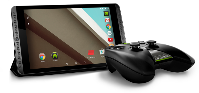
The first part of the announcement is the announcement of the release date for the update to Android Lollipop. NVIDIA plans to begin the rollout of the update on Tuesday, November 18th, less than one week from today. Although NVIDIA is not the first manufacturer to begin to ship the Lollipop update, the speed at which they have done so is still extremely fast relative to how long it typically takes Android devices to receive updates. It's also impressive because NVIDIA has had to spend time updating their included applications like SHIELD Hub to follow Google's Material Design principles.
In addition to the Lollipop update, NVIDIA will also be including a substantial update for their Dabbler app, bringing it to version 2.0. For users who don't know, Dabbler is a sketching application that NVIDIA makes for the SHIELD Tablet to work with the stylus. Users who are familiar with Paper by FiftyThree for iPad will have an idea of what Dabbler is, but with Dabbler 2.0 NVIDIA is bringing a substantial improvement to the application with support for multiple layers in images, along with a new Material Design appearance. The addition of layers is only a single feature, but it brings Dabbler much closer to the features we see in professional art applications. Dabbler 2.0 also brings support for Twitch streaming so users can stream their drawing sessions, allowing users to watch the sketch being created.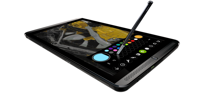
The appeal of the SHIELD Tablet is its capability for playing games. Not just mobile games, but also a collection of PC games that NVIDIA has worked with game developers to bring over to SHIELD devices. Portal and Half Life 2 have already been available for some time now, but as you'll see above there's a new addition to the library of Valve games available for SHIELD, with Half Life 2: Episode One being made available for the platform. It will be available for purchase on its own to current owners, and it will also be available alongside Half Life 2 and Portal in a bundle called the Green Box, which will come free with the LTE model of the SHIELD Tablet. All that's left is to bring Half Life 2: Episode 2, and the SHIELD tablet will have all of the released titles in Valve's eternally incomplete set of episodic games.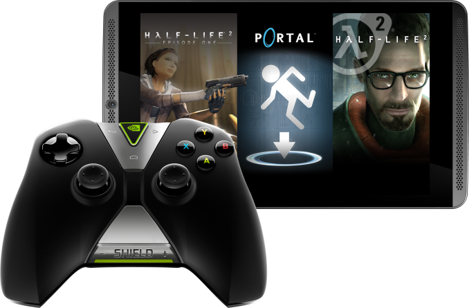
In addition to Half Life 2: Episode 1, NVIDIA is telling users to keep an eye out for three new SHIELD-optimized games that are available on Google Play. The first is OddWorld: Stranger's Wrath which is an action-adventure game. The second is Pure Pool, which allows users to play pool with high quality 3D graphics. The third and final is Strike Suit Zero which is a space combat game.
The last, and possibly most exciting announcement of the day from NVIDIA, is the expansion of their GRID cloud gaming service. The idea of a cloud based service for streaming games is nothing new, and we're frequently promised that one that works well is right on the horizon, but it has remained fairly elusive. Based on the feedback from the beta that NVIDIA has been conducting in the Western U.S. with servers located in San Jose, California, GRID looks like it might be the first service to actually deliver on the promise of being able to stream your games over the net to a device that it could never be run on locally with good quality and minimal input lag. The service currently has over 20 AAA titles, including Batman Arkham City, Borderlands 2, and Psychonauts, with NVIDIA committing to add new games every week.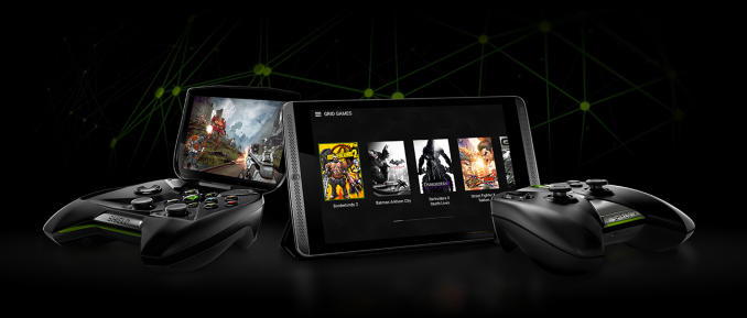
After conducting their beta in California, NVIDIA seems ready to begin expanding the service to other places around the world. The service will be available in North America by the end of this month, in Western Europe in December, and in Asia during the second quarter of 2015. It will be available on the SHIELD Tablet and original SHIELD portable, and best of all, until June 30, 2015 it will be available for free.
More...
-
11-15-14, 08:30 AM #4494
Anandtech: Sponsored Post: ARM Wearables Week
The incredible rise of the smartphone market was a phenomena that caught virtually everyone off-guard. Though cellular phones had been ramping up in complexity for nearly 20 years, the sudden jump in consumer demand from “dumb” to “smart” is virtually unprecedented; very few technologies have been so thoroughly adopted in such a short period of time. At the center of all of this was ARM, whose processors and architecture powered nearly every single phone at the heart of the smartphone revolution.
Now with mobile device sales stabilizing and devices approaching “good enough” status, the consumer electronics industry finds itself looking at the future and what comes next. Looking to repeat the smartphone revolution, all eyes are on wearable computing, which is looking to build off of the technologies and lessons of smartphones to start bringing some of that processing power and functionality into some of the smallest and most personal devices yet.
As part of the broader conversation and development of wearables, next week ARM will be holding their ARM Wearables Week event. For this event ARM will be focusing on the technical issues facing wearables and how they can solve them – processing power, battery life, and meeting those aforementioned needs while fitting the entire package in an acceptable form factor. With Cortex-M and mbed among the many tools in their portfolio, ARM believes that the technology is right and the time is right for wearables to take off.
Highlights of the week will include interviews with industry experts and the Wearables Week Webinar with Omate, which will be providing a case study for wearables by looking at the development of Omate’s products. ARM will also be doing teardowns of various wearable devices such as the Samsung Galaxy Gear 2 Neo and LG G, to show how these devices are put together.
So be sure to check out the ARM Wearables Week website for the above and more as ARM continues to roll out new content throughout the week.
More...
-
11-15-14, 01:31 PM #4495
Anandtech: Exploring Performance Consistency in USB 3.0 Flash Drives
SSD technology has advanced to a stage where it is possible to have flash drives with bona-fide SSD controllers. The addition of a SATA to USB 3.0 bridge provides an ubiquitous high-speed direct attached storage interface. We have already looked at the Phison S9-based Corsair Flash Voyager GTX and the SandForce SF2281-based Mushkin Ventura Ultra. Our review of the Mushkin Ventura Ultra 120GB drive had a comment about the device's thermal throttling issues. This piqued our interest and we set out to see if any of the other units evaluated before had such issues. Obviously, we were also interested in determining whether our Ventura Ultra sample had the problem. In the case of throttling, we also wanted to make our review complete by bringing out the circumstances under which it would trigger. As we will see further down in this piece, our experiments did find evidence of throttling in the Mushkin Ventura Ultra.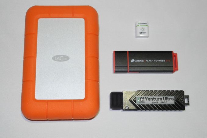
Recently, we also received a sample of another SSD controller-based flash drive. Putting that drive through our throttling test revealed even worse results compared to the Mushkin Ventura Ultra. Upon our feedback, the manufacturer is contemplating a firmware update. In this piece, we will refer to the unit as 'BrandX 240GB' (a complete review of the unit with benchmark numbers will be published once the manufacturer provides us a resolution for the throttling issue). The list of DAS units put under the performance consistency scanner is provided below.
- Mushkin Ventura Ultra 120GB
- BrandX 240GB
- Corsair Voyager GTX 256GB
- LaCie Rugged Thunderbolt 500GB
- Mushkin Atom 64GB
Performance Consistency Evaluation Methodology
Our testing methodology for DAS units takes into consideration the usual use-case for such devices. The most common usage scenario is transfer of large amounts of photos and videos to and from the unit. In order to tackle this, we created three test folders with the following characteristics:
- Photos: 15.6 GB collection of 4320 photos (RAW as well as JPEGs) in 61 sub-folders
- Videos: 16.1 GB collection of 244 videos (MP4 as well as MOVs) in 6 sub-folders
- BR: 10.7 GB Blu-ray folder structure of the IDT Benchmark Blu-ray (the same that we use in our robocopy tests for NAS systems)
These folders were put in a RAM drive on our testbed. Using robocopy, each folder was copied from the RAM drive to the DAS (write benchmark) and back to the RAM drive (read benchmark). This process was repeated thrice. To check for performance consistency, we instrumented our benchmark script to record the flash drive's read and write transfer rates while the robocopy process took place in the background. For supported drives, we also recorded the internal temperature of the drive during the process.
Evaluation Results
Aspects that may influence performance consistency include thermal throttling and firmware caps on access rates to avoid overheating or other similar scenarios. This aspect is an important one, as the last thing that users want to see when copying over, say, 100 GB of data to the flash drive, is the transfer rate going to USB 2.0 speeds. The graphs below show the speeds observed during our real-world DAS suite processing with the instrumented benchmark script. The first three sets of writes and reads correspond to the photos suite. A small gap (for the transfer of the videos suite from the primary drive to the RAM drive) is followed by three sets for the next data set. Another small RAM-drive transfer gap is followed by three sets for the Blu-ray folder.
An important point to note here is that each of the first three blue and green areas correspond to 15.6 GB of writes and reads respectively. Throttling, if any, is apparent within the processing of the photos suite itself.
Mushkin Ventura Ultra 120GBBrandX 240GBCorsair Voyager GTX 256GBLaCie Rugged Thunderbolt 500GBMushkin Atom 64GBThe Mushkin Ventura Ultra 120GB does throttle after the S.M.A.R.T temperature report reaches 45 C. In our testbed (ambient at 22C), this temperature was reached after approximately 18 GB of writes and 16 GB of reads without any interruptions. Beyond this, the write speeds got capped around 80 MBps (compared to the non-throttled 100 MBps), while the reads got capped around 100 MBps (compared to the non-throttled 140 MBps). The throttling allowed the temperature to stay below 50 C throughout our benchmark run.
BrandX, though, behaved differently. The temperature in the steady state settled around 53 C. Unfortunately, the throttling (after a similar amount of data transfer as the Mushkin Ventura Ultra) resulted in the write speeds getting capped at a paltry 20 MBps. The reads managed to remain around 80 MBps.
The Mushkin Atom is not meant to take the performance crown, and the advertised write speeds are in the 20 MBps range. Our benchmark run ran at a steady 15 MBps, while the reads didn't get throttled at all in our evaluation process.
The LaCie Rugged Thunderbolt drive is not a flash drive (unlike the other units considered in this piece). It is a bona-fide SSD in a USB 3.0 / Thunderbolt hybrid enclosure. It is no wonder that the transfer rates were hardly affected by the relatively small amount of data traffic. The real winner of our evaluation was the Corsair Voyager GTX. There is no performance degradation even after more than 120 GB of continuous traffic. It must also be remembered that we ran our robocopy benchmark with multiple queue depths in our original review (that was more than 480 GB of continuous traffic) and the table showed remarkable consistency. The instrumented benchmark run confirmed the same.
Concluding Remarks
Coming to the business end of the piece, it must be remembered that the capabilities must be compared keeping the price in mind. If cost is not an issue and the form factor is not an issue, the LaCie Rugged Thunderbolt is the hands down winner for a fast portable DAS unit with consistent performance. If cost is the primary concern, and one doesn't mind a little bit of throttling after around 18 GB of continuous write traffic, the Mushkin Ventura Ultra is a great choice at less than $0.6/GB. The middle ground (right balance of cost and fast, consistent performance, along with a traditional flash drive form factor) is held by the Corsair Voyager GTX. At more than $0.85/GB, it also serves as a reminder that one gets what they pay for.
More...
-
11-17-14, 07:12 AM #4496
Anandtech: NVIDIA Volta, IBM POWER9 Land Contracts For New US Government Supercompute
The launch of Oak Ridge National Laboratory’s Titan Supercomputer was in many ways a turning point for NVIDIA’s GPU compute business. Though already into their third generation of Tesla products by that time, getting Tesla into the world’s most powerful supercomputer is as much of a singular mark of “making it” as there can be. Supercomputer contracts are not just large orders in and of themselves, but they indicate that the HPC industry has accepted GPUs as reliable and performant, and is ready to significantly invest in them. Since then Tesla has ended up in several other supercomputer contracts, with Tesla K20 systems powering 2 of the world’s top 10 supercomputers, and Tesla sales overall for this generation have greatly surpassed the Fermi generation.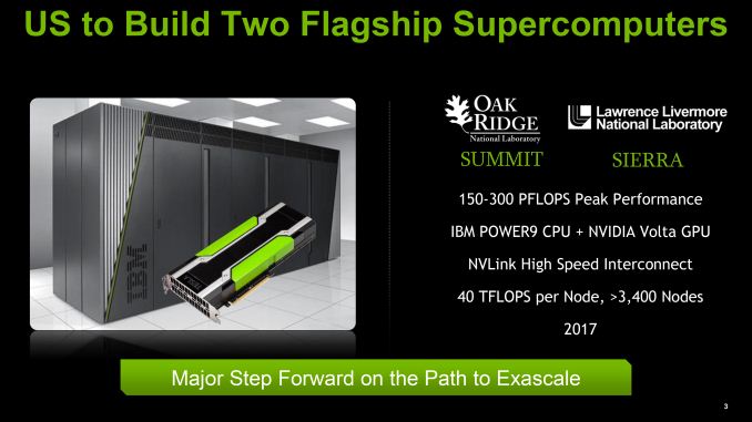
Of course while landing their first supercomputer contract was a major accomplishment for NVIDIA, it’s not the only factor in making the current success of Tesla a sustainable success. To steal a restaurant analogy, NVIDIA was able to get customers in the door, but could they get them to come back? As announced by the US Department of Energy at the end of last week the answer to that is yes. The DoE is building 2 more supercomputers, and it will be NVIDIA and IBM powering them.
The two supercomputers will be Summit and Sierra. At a combined price tag of $325 million, the supercomputers will be built by IBM for Oak Ridge National Laboratory and Lawrence Livermore National Laboratory respectively. They will be the successors to the laboratories respective current supercomputers, Titan and Sequoia.
Hardware
Both systems will be of similar design, with Summit being the more powerful of the two. Powering the systems will be a triumvirate of technologies; IBM POWER9 CPUs, NVIDIA Volta-based Tesla GPUs, and Mellanox EDR Infiniband for the system interconnect.
Starting with the CPU, at this point this is the first real attention POWER9 has received. Relatively little information is available on the CPU, though IBM has previously mentioned that POWER9 is going to emphasize the use of accelerators (specialist hardware), which meshes well with what is being done for these supercomputers. Otherwise beyond this we don’t know much else other than that it will be building on top of IBM’s existing POWER8 technologies.
Meanwhile on the GPU side, this supercomputer announcement marks the reintroduction of Volta by NVIDIA since going quiet on it after the announcement of Pascal earlier this year. Volta was then and still remains a blank slate, so not unlike the POWER9 CPU we don’t know what new functionality is due with Volta, only that it is a distinct product that is separate from Pascal and that it will be building off of Pascal. Pascal of course introduces support for 3D stacked memory and NVLink, both of which will be critical for these supercomputers.
Speaking of NVLink, as IBM’s POWER family is the first CPU family to support NVLink it should come as no surprise that NVLink will be the CPU-GPU and GPU-GPU interconnect for these computers. NVIDIA’s high-speed PCIe replacement, NVLink is intended to allow faster, lower latency, and lower energy communication between processors, and is expected to play a big part in NVIDIA’s HPC performance goals. While GPU-GPU NVLink has been expected to reach production systems from day one, the DoE supercomputer announcement means that the CPU-GPU implementation is also becoming reality. Until now it was unknown whether an NVLink equipped POWER CPU would be manufactured (it was merely an option to licensees), so this confirms that we’ll be seeing NVLink CPUs as well as GPUs.
With NVLink in place for CPU-GPU communications these supercomputers will be able to offer unified memory support, which should go a long way towards opening up these systems to tasks that require frequent CPU/GPU interaction, as opposed to the more homogenous nature of systems such as Titan. Meanwhile it is likely – though unconfirmed – that these systems will be using NVLink 2.0, which as originally announced was expected for the GPU after Pascal. NVLink 2.0 introduces cache coherency, which would allow for further performance improvements and the ability to more readily execute programs in a heterogeneous manner.
SystemsThough similar in design, the total computational power and respective workloads will differ for Summit and Sierra. Sierra, the smaller of the systems, is to be delivered to Lawrence Livermore National Laboratory to replace their current 20 PetaFLOP Sequoia supercomputer. LLNL will be using Sierra for the National Nuclear Security Administration’s ongoing nuclear weapon simulations, with LLNL noting that “the machine will be dedicated to high-resolution weapons science and uncertainty quantification for weapons assessment.”US Department of Energy Supercomputers Summit Titan Sierra Sequoia CPU Architecture IBM POWER9 AMD Opteron
(Bulldozer)IBM POWER9 IBM BlueGene/Q GPU Architecture NVIDIA Volta NVIDIA Kepler NVIDIA Volta N/A Performance (RPEAK) 150 - 300 PFLOPS 27 PFLOPS 100+ PFLOPS 20 PFLOPS Power Consumption ~10MW ~9MW N/A ~8MW Nodes 3,400 18,688 N/A N/A Laboratory Oak Ridge Oak Ridge Lawrence Livermore Lawrence Livermore Vendor IBM Cray IBM IBM
Due to its use in nuclear weapons simulations, information on Sierra is more restricted than it is for Summit. Publicly, Sierra is being quoted as offering 100+ PFLOPS of performance, over five-times the performance of Sequoia. As these supercomputers are still in development the final performance figures are unknown – power consumption and clockspeed cannot be guaranteed this early in the process, not to mention performance scaling on such a large system – and it is likely Sierra will exceed its 100 PFLOPS performance floor.
Sierra: 100+ PetaFLOPS
Meanwhile the more powerful of the systems, Summit, will be delivered to the Oak Ridge National Laboratory. In building their current Titan supercomputer, ORNL expected to get 4-5 years out of Titan, and adhering to that schedule Summit will be Titan’s replacement.
Summit’s performance is expected to be in the 150-300 PFLOPS range, once again varying depending on the final clockspeeds and attainable performance of the cluster. In 2012 ORNL wanted their next system to offer 10x the performance of Titan, and at this point Summit’s performance estimates range from 5x to 10x Titan, so while not guaranteed at this time it is still a possibility that Summit will hit that 10x goal.
Summit: 150 to 300 PetaFLOPS
As Summit is geared towards public work, we know quite a bit more about its construction than we do Seirra. Summit will be built out of roughly 3400 nodes, with each node containing multiple CPUs and GPUs (as opposed to 1 of each per Titan node). Each node in turn will be backed by at least 512GB of memory, most likely composed of 512GB of DDR4 and a to-be-determined amount of High Bandwidth Memory (stacked memory) on each GPU. Backing that in turn will be another 800GB of NVRAM per node.
From a power standpoint Summit is expected to draw 10MW peak, roughly 10% higher than Titan’s 9MW. However despite the slight increase in power consumption Summit is expected to physically be far smaller than Titan. With Summit nodes taking up roughly the same amount of space as Titan nodes, Summit’s node will occupy around only 20% of Titan’s nodes. Key to this of course is increasing the number of processors per node; along with multiple CPUs per node, NVIDIA’s new mezzanine form factor GPUs would play a large part here, as they allow for GPUs to be installed and cooled in a fashion similar to socketed CPUs.
Like Titan before it, Summit will be dedicated to what ORNL calls “open science.” Time on the supercomputer will be granted to researchers through application proposals. Much of the science expected to be done on Summit is similar to the science already done on Titan – climate simulations, (astro)physics, nuclear, etc – with Summit’s greater performance allowing for more intricate simulations.
NVIDIA Pascal Test Vehicle Showing New GPU Form Factor
Finally, Summit is expected to come online in 2017, with trials and qualifications leading up to the machine being opened to users in 2018. As it stands, when Summit launches it will be the most powerful supercomputer in the world. Its 150 PLFOPS lower bound being roughly 3x faster than the current record holder, China’s Xeon Phi powered Tianhe-2, and no other supercomputers have been announced (yet) that are expected to surpass that number.
Wrapping things up, for both IBM and NVIDIA securing new supercomputer contracts is a major win. With IBM indirectly scaling back its role in the supercomputer race – BlueGene/Q being the last of the BlueGenes – IBM will continue providing supercomputers by providing heterogeneous powered by a mix of their own hardware and NVIDIA GPUs. NVIIDA of course is no less thrilled to be in not only the successor to Titan, but in another DoE lab’s supercomputer as well, and with a greater share of the underlying technology than before.
Though with that said, it should be noted that this is not the last major supercomputer order the DoE will be placing. The CORAL project for these supercomputers also includes a supercomputer for Argonne National Laboratory, who will be replacing their Mira supercomputer in the same timeframe. The details for that supercomputer will be announced at a later date, so there is still one more supercomputer contract to be awarded.
More...
-
11-17-14, 08:37 AM #4497
Anandtech: NVIDIA Launches Tesla K80, GK210 GPU
Kicking off today is the annual International Conference for High Performance Computing, Networking, Storage, and Analysis, better known as SC. For NVIDIA, next to their annual GPU Technology Conference, SC is their second biggest GPU compute conference, and is typically the venue for NVIDIA’s summer/fall announcements. Earlier we covered the announcement of NVIDIA’s role in the US Department of Energy’s latest supercomputer acquisitions, and today we’ll be taking a look at NVIDIA’s latest Tesla GPU compute card, Tesla K80.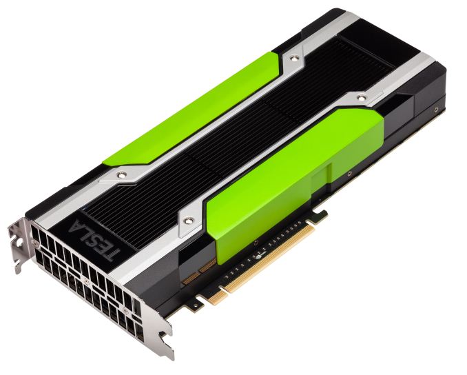
At SC’13 NVIDIA introduced the Tesla K40, the first “fully enabled” Kepler Tesla card. Based on the GK110B variant of NVIDA’s GPU, this was the first Tesla product to ship with all 2880 CUDA cores enabled. Typically one would think that with a fully enabled GK110 based board that the Kepler Tesla lineup would have reached its apex, but for SC’14 NVIDIA will be pushing the performance envelope a bit harder in order to produce their fastest (and densest) Tesla card yet.
Dubbed the Tesla K80, NVIDIA’s latest Tesla card is an unusual and unexpected entry into the Tesla lineup. For Tesla K80 NVIDIA has produced a new GPU – GK210 – and then put two of them into a single card. The net result is a card with no peers; NVIDIA has done dual GPU Tesla cards before (Tesla K10) and there have been dual GPU GK110 cards before (GeForce Titan Z), but nothing quite like Tesla K80.NVIDIA Tesla Family Specification Comparison Tesla K80 Tesla K40 Tesla K20X Tesla K20 Stream Processors 2 x 2496 2880 2688 2496 Core Clock 562MHz 745MHz 732MHz 706MHz Boost Clock(s) 875MHz 810MHz, 875MHz N/A N/A Memory Clock 5GHz GDDR5 6GHz GDDR5 5.2GHz GDDR5 5.2GHz GDDR5 Memory Bus Width 2 x 384-bit 384-bit 384-bit 320-bit VRAM 2 x 12GB 12GB 6GB 5GB Single Precision 8.74 TFLOPS 4.29 TFLOPS 3.95 TFLOPS 3.52 TFLOPS Double Precision 2.91 TFLOPS (1/3) 1.43 TFLOPS (1/3) 1.31 TFLOPS (1/3) 1.17 TFLOPS (1/3) Transistor Count 2 x 7.1B(?) 7.1B 7.1B 7.1B TDP 300W 235W 235W 225W Cooling Passive Active/Passive Passive Active/Passive Manufacturing Process TSMC 28nm TSMC 28nm TSMC 28nm TSMC 28nm Architecture Kepler Kepler Kepler Kepler Launch Price N/A $5499? ~$3799 ~$3299
From both a performance and power standpoint, NVIDIA is expecting to once again raise the bar. Factoring in GPU Boost (more on that later), Tesla K80 is rated for a maximum double precision (FP64) throughput of 2.9 TFLOPS, or a single precision (FP32) throughput of 8.7 TFLOPS. Compared to Tesla K40 this is roughly 74% faster than NVIDIA’s previous top-tier Tesla card, though GPU Boost means that the real performance advantage will not reach quite that high.
Fitting a pair of GPUs on a single card is not easy, and that is especially the case when those GPUs are GK210. Unsurprisingly then, NVIDIA is shipping K80 with only 13 of 15 SMXes enabled on each GPU, for a combined total of 4,992 CUDA cores enabled. This puts the clockspeed at a range of 562MHz to 870MHz. Meanwhile the memory clockspeeds have also been turned down slightly from Tesla K40; for Tesla K80 each GPU is paired with 12GB of GDDR5 clocked at 5GHz, for 240GB/sec of memory bandwidth per GPU. This puts the total memory pool between the two GPUs at 12GB, with 480GB/sec of bandwidth among them.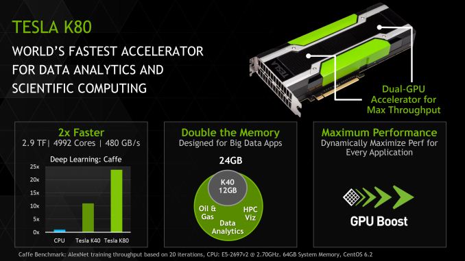
Meanwhile Tesla K80 will also be pushing the power envelope, again to get 2 GPUs on a single card. Whereas Tesla K80 and K20X were 235W cards, Tesla K80 is a 300W card. The fact that NVIDIA was able to get two high performance GPUs within 300W is no small achievement in and of itself, though for this reason GPU Boost plays a big part in making the overall product viable. Consequently energy efficiency gains are almost entirely reliant on what kind of performance Tesla K80 can sustain at 300W; the worst case scenario is that it’s only 2% more energy efficient than K40 while the best case is 59%, with the realistic case being somewhere in the middle.
Speaking of efficiency, for Tesla K80 NVIDIA has crammed it into a standard size double-slot Tesla card enclosure, so on a volume basis Tesla K80 packs quite a bit more power per slot than K40, improving NVIDIA’s space efficiency. So far we have only seen passive cards, and given the need to move 300W of heat we expect that these cards will need to be passive in order to be paired up with appropriately powerful external fans.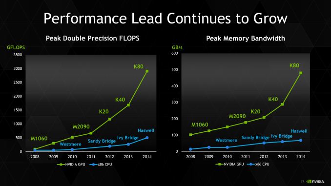
Moving on, let’s start with GK210. Introduced with Tesla K80, GK210 is fundamentally the 3rd revision of GK110, following in the footsteps of GK110B, introduced on Tesla K40. Compared to GK110B, which was really just a cleanup of GK110, GK210 is a more radical alteration of GK110. This time around NVIDIA has made some real feature changes that although maintain GK210’s lineage from GK110, none the less make it meaningfully different from its predecessor.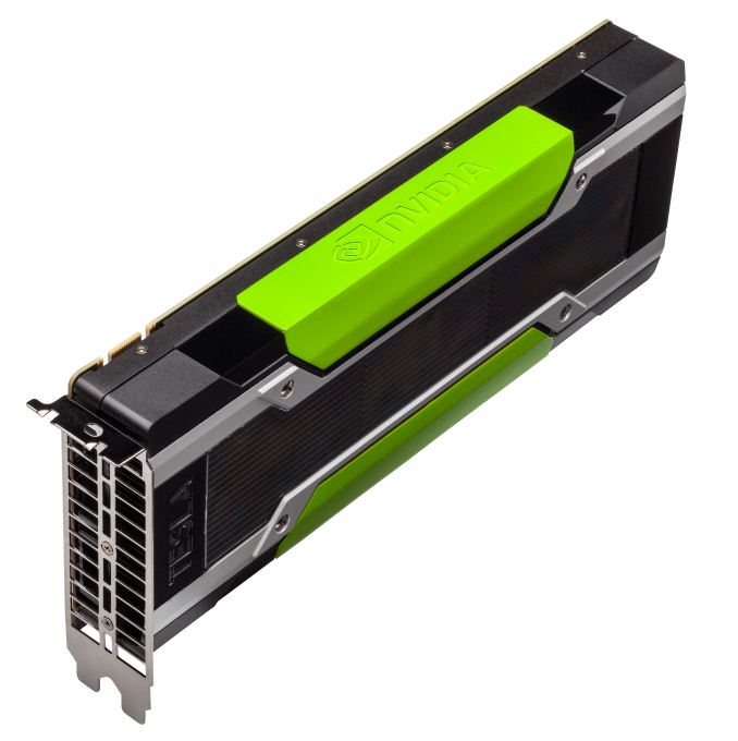
To that end, while NVIDIA hasn’t made any sweeping changes such as adjusting the number of CUDA cores or their organization (this is still a GK110 derivative, after all) NVIDIA has adjusted the memory subsystem in each SMX. Whereas a GK110(B) SMX has a 256KB register file and 64KB of shared memory, GK210 doubles that to a 512KB register file and 128KB of shared memory. Though small, this change improves the data throughput within an SMX, serving to improve efficiency and keep the CUDA cores working more often. NVIDIA has never made a change mid-stream like this to a GPU before, so this marks the first time we’ve seen a GPU altered in a later revision in this fashion. That said, this also reflects on the state of the GPU market, and how Kepler will still be with us for some time to come.GK110 Family GPUs GK210 GK110B GK110 Stream Processors 2880 2880 2880 Memory Bus Width 384-bit 384-bit 384-bit Register File Size 512KB 256KB 256KB Shared Memory /
L1 Cache128KB 64KB 64KB Transistor Count 7.1B(?) 7.1B 7.1B Manufacturing Process TSMC 28nm TSMC 28nm TSMC 28nm Architecture Kepler Kepler Kepler Tesla Products K80 K40 K20/K20X
Overall I suspect that along with the memory change, NVIDIA has used this latest revision to once again tighten up the design of their HPC GPU to correct errata and reduce power consumption (thereby improving performance), which is part of the reason that NVIDIA is able to get two of these GPUs in a 300W card. Meanwhile GK210 will be in an odd place as it will likely be the first NVIDIA GPU not to end up in a consumer card; prior to this generation every GPU has pulled double duty as both a compute powerhouse and a graphics king. But with GM204 clearly ahead of GK110/GK210 in graphics, GK210 seems destined to Tesla cards and at most a Titan card for the budget compute market. Given the costs in bringing a new GPU revision to market – just the masks alone are increasingly expensive – the situation implies that NVIDIA expects to more than make back their money on additional sales enabled by GK210, which in turn indicates that they have quite a bit of faith in the state of the GPU compute market since it alone would be where the additional revenue would come from.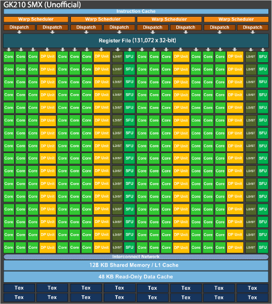
The final piece of the puzzle for Tesla K80 is GPU Boost. In the Tesla space NVIDIA introduced this on Tesla K40 in a far more limited implementation than on their consumer GPUs. Tesla K40 had to obey its TDP, but operators could select which of 3 clockspeeds they wanted, picking the one that comes closest to (but not exceeding) TDP for the best performance. However with Tesla K80 NVIDIA has now implemented a full and dynamic GPU boost implementation; just as in their consumer cards, the card will clock itself as high as the TDP will allow.
The change in implementation is no doubt driven by the more complex thermal environment of a multi-GPU card, not to mention the need to squeeze out yet more efficiency. As with consumer cards TDP headroom left on the table is potential performance wasted, and for Tesla this is no different. Without GPU boost and building to a worst case scenario, K80 would not be much more efficient than K40, as evidenced by the 562MHz core clockspeed. That said, with K40 NVIDIA made clockspeeds deterministic for GPU workload sync issues, so it’s not entirely clear why non-deterministic clockspeeds are now okay just a year later.
Specifications aside, Tesla K80 represents an unexpected evolution in Tesla designs. Strictly speaking, Tesla K80 is often but not always superior to Tesla K40. Per GPU throughput is lower than on Tesla K40, so given a task that doesn’t scale well over multiple GPUs a Tesla K40 could still be faster. None the less, the majority of tasks Tesla cards will run will cleanly scale well over multiple GPUs – this being a cornerstone of the modern HPC paradigm of clusters of processors – so outside of a few edge cases K80 should be faster, generally quite a bit faster.
Otherwise the density implications are quite interesting. A 300W TDP presents its own challenges, but in surmounting that it’s now possible to get 8 GK210 GPUs in a 1U form factor, which would put the FP64 compute throughput of such a setup at over 10 TFLOPS in 1U.
Wrapping things up, Tesla K80 will be a hard launch from NVIDIA and their partners, with individual cards and OEM systems equipped with them expected to be available today. Officially NVIIDA does not publish MSRPs for Tesla cards and we have not seen any listed as of press time, so we do not know what the K80 will sell for. However packing two GPUs it’s almost certainly going to launch at more than the roughly $5500 that K40 launched at a year ago.

More...
-
11-17-14, 08:37 AM #4498
Anandtech: Corsair Neutron XT (240GB, 480GB & 960GB) SSD Review: Phison S10 Debuts
The ugly truth is that the SSD market has been tough for almost all the typical PC component vendors lately. With Samsung, SanDisk and Micron/Crucial being serious about the client market, it is not easy for the rest to find a way to provide any substantial advantage over the big brands. The fab owners will always enjoy a cost advantage, which is why we have seen a few companies backing off from the market and many more for whom SSDs have become just another series in the pool of products. This is what could be said to have happened at Corsair. While the company has never been super aggressive on the SSD side, the past year or so has been very quiet, but that changes with the Neutron XT. Read on to find out more about Corsair's latest SSD and the launch vehicle of Phison's brand new S10 controller.
More...
-
11-18-14, 12:01 AM #4499
Anandtech: Intel Plans Merger Of Mobile And PC Divisions
According to a report this evening from the Wall Street Journal, in an email sent to employees by Intel CEO Brian Krzanich, Intel has announced plans to merge their struggling Mobile division with the PC Division. The newly created Client Computing Group would be led by Kirk Skaugen, who currently heads the PC division for Intel. The change in reporting is announced to commence in the beginning of calendar year 2015.
The Mobile and Communications Group, which currently is responsible for tablet and smartphone platforms as well as RF transceivers, GPS, Wi-Fi, and Bluetooth will be broken up. The teams which focus on SoC development will join the Client Computing Group, and those which focus on RF technologies will form a new wireless R&D group.
As we reported in Intel’s most recent earnings report, the Mobile and Communications Group had an operating loss of $1.043 billion for Q3 2014. Intel had a goal of putting Atom in to 40 million tablets in 2014, and the plan to do this was to offset the costs of using Bay Trail instead of ARM SoCs, as well as help cover the engineering costs of moving to an Intel platform. While Intel is on track to exceed the original 40 million goal, it has done it at the cost of just over $3 billion to the Mobile and Communications Group bottom line for the nine months ended September 27th.
While this may seem at first glance as a way to move the losses into a profitable division, Intel has not yet decided whether the new divisions will be reflected in their financial reporting structure. So clearly this is not just about the numbers. What this appears to mean is that mobile and desktop will now be given the same priority, and possibly the same access to fabs. In the past, the newest fab nodes have been available for the Core processors first, with the lower margin Atom processors getting access at a later date. The Core processors moved to the Tick-Tock design process where each year a Die shrink (Tick) is alternated with a new microarchitecture (Tock) in 2006, but the Atom processor has just had its first new microarchitecture since 2008 with Silvermont replacing Bonnell. This puts Atom on 22 nm, and a schedule to move to 14 nm in 2015 with Airmont.
On the Core side, the Tick Tock strategy has been almost flawless, with Intel now dominating desktop processor benchmarks and sales. The strategy would likely work well for the mobile sector as well if it had been started several years ago. According to Chuck Malloy, a spokesman for Intel, “The idea is to accelerate the implementation and create some efficiency so that we can move even faster.”
At the same time this may also be a sign that Intel is reevaluating their chip design strategy, and where the line is drawn between Atom and Core. While Silvermont has proven to be no slouch, it is still a mobile focused chip with a narrow pipeline, as opposed to the wider pipeline, higher IPC designs of the Core family. In that sense Core has so far been something of a premium brand for Intel, reserved for higher value (higher margin) devices while Atom has gone into cheaper devices.
If Intel were to shift Core-like high-IPC designs into the Atom family - a distinct possibiltiy now that development for both is under the same roof - that could have a significant impact on Intel’s performance in the mobile market. Apple has already pursued a variant of this strategy to great effect, their Cyclone family of CPUs being very Core-like in design and frequently topping the performance charts in the process. However in the process Apple has thrown some very large (120mm2+) SoCs into their devices, something that helps their performance but would certainly give margin-centric Intel pause for thought.
Overall, although details are light this could signal a big change in the way Intel does business. If mobile gets the same sort of priority as the flagship Core series and the same sort of top-tier architectures, this could be of great benefit to Intel's CPU performance in the mobile space. At the same time, the PC division may also benefit from some of the mobile experience. As we have seen with Core M, Intel has focused a lot on overall package size and thickness. Moving the expertise in that area into the same division as the people responsible for the Core series could have benefits as well.
With this change just coming into effect at the start of 2015, it will not likely have any impact on Skylake or Airmont, however we could see some synergy in the follow up products.
Source: Wall Street Journal, Bloomberg, PCWorld
More...
-
11-18-14, 05:42 AM #4500
Anandtech: Synology DS1815+ 8-bay Intel Rangeley SMB NAS Review
Synology started the roll-out of their SMB-targeted NAS units based on Intel's latest Atom platform (Rangeley) in September 2014. We have already looked at the 4-bay DS415+ in detail. Today, the 5-bay and 8-bay versions are being officially launched. Read on for our review to find out how Intel's Rangeley platform and Synology's DSM perform in a 8-bay configuration.
More...


 Quote
QuoteThread Information
Users Browsing this Thread
There are currently 12 users browsing this thread. (0 members and 12 guests)


Bookmarks