

Results 4,751 to 4,760 of 12091
Thread: Anandtech News
-
02-18-15, 03:32 PM #4751
Anandtech: Samsung Acquires Mobile Payment Company LoopPay
Today the US based mobile payment company LoopPay announced that they have been acquired by Samsung Electronics America. LoopPay is a unique example of a payment company that is building their payment system on top of the existing magnetic stripe payment infrastructure that currently exists in the US, rather than using NFC technology which can require waiting for retailer support and the purchase of new payment terminals for stores. Currently the company offers several smartphone cases as well as a keychain fob, and these devices wirelessly interface with the magnetic stripe readers on payment terminals. It will be interesting to see how Samsung integrates LoopPay's technology into future products, and how they will handle expansion outside of the US where many countries have switched to chip and pin readers.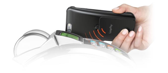
More...
-
02-19-15, 09:02 AM #4752
Anandtech: Dell XPS 13 Review
Dell launched the 2015 version of their XPS 13 at CES in January, and it made a big impression because of something that was very small. The first thing you see when you look at the XPS 13 is how small the bezels are around the display. At 5.2 mm, they are easily the thinnest display bezels on any laptop made today. Dell claims the XPS 13 is a 13 inch display in the chassis of an 11 inch notebook, and while they have made that claim before, for 2015, it would be hard to argue with them. But the XPS 13 is more than just a display, and Dell has outfitted it with some very modern hardware to give us our first look at an Ultrabook based on the just launched Intel 5th Generation processors, Broadwell-U.
More...
-
02-19-15, 06:03 PM #4753
Anandtech: Lenovo, SuperFish and Security
For the many of us that have purchased a laptop, we are somewhat used to the amount of bloatware that comes pre-installed. Most of this relates to the company specific software, or free trials for office applications or anti-virus software. I would imagine that the more technologically savvy users uninstall some of this bloat for themselves and their family and friends, but it does give an opportunity for the manufacturer to install what they want before the device gets shipped.
Here at AnandTech we receive laptops on a regular basis for review, and where we can we tend to ask for retail units so we can analyze the hardware without fear of getting a ‘review-focused’ sample. The same thing goes for motherboards, SSDs, and graphics cards, which also come with their own software but the user has to specifically install everything. With a laptop, smartphone, tablet, workstation, or notebook, it all comes pre-prepared for the user to plug and play. The demand to remove the bloatware has led to smartphones and tablets being offered with pure stock versions but also carrier customized ones, and some users get the choice of both.
A topic that has been in the news today, and whose symptoms date back a little further, has been with Lenovo laptops and notebooks. This software is called SuperFish and comes as a browser add-on, which Lenovo calls a ‘Visual Discover’ program that detects when a website has advertising and replaces it with targeted images based on what the user is looking at in order to make informed choices at potentially lower prices. This comes with a variety of issues.
First, it replaces the advertisement(s) on the website, which offers the website a form of income (such as AnandTech and other advertiser driven models). The new advertisement redirects the link to a server that may benefit Lenovo, distorting the ad views for that particular website and shifting income back to the laptop manufacturer.
Second, SuperFish is actively scanning the websites that people look at, resulting in privacy issues. Lenovo has stated that this software analyzes images in an algorithmic pattern (presumably similar to Google Goggles) rather than tracking the behavior of the user, but without access to the code most users will still not trust the software. After consistent issues regarding security and tracking in the media recently, especially with certain ‘Smart TVs’, it is understandable how users do not want to live in a 1984 type of environment.
Third, the best explanation for SuperFish comes down as adware. Malware and adware have been a common threat of the century when it comes to web browsing, where software places unwanted advertisements in the eye-line of the user to generate revenue. If we take that definition then SuperFish falls under that category, no matter how it is dressed up.
The fourth issue revolves around surrounding security. This is twofold – the SuperFish software will break any HTTPS encrypted webpage that has advertisements when it replaces them with its own, creating a mix of secure and insecure content. This allows other software to come in and potentially inject its own attack, stealing sensitive information. The second issue with security is that SuperFish issues its own SSL certificates for a large number of common sites, with severely reduced security than what is often required, such as with banks with the example that is circling the internet:
This essentially amounts to a fake certificate, giving SuperFish access to your private information. Any and all alarm bells should be ringing in everyone’s ears at this point, as this means potential access to bank information, personal information, and any other sensitive information. These certificates are accepted because Lenovo has pre-installed the PC with details to accept SuperFish certificates, essentially creating a 'self-signing authority'. As SuperFish is monitoring the images contained within the ‘secure’ webpages, a classic man-in-the-middle attack by most adware software, if they are tracing that information it could end up in the hands of someone else. SuperFish does not tell the user if the official certificate has been replaced, and the same encryption-key based certificate is used for each site, meaning that other tools that manage to break one certificate can break them all.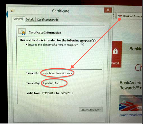
To add insult to injury, the security of these certificates would seem to be using SHA-1, which is insecure and can be overcome with the right software and ordinary computing hardware. The 1024-bit RSA key has also been cracked, with the private key being bundled with the software in order to execute on-the-fly digital certificate signing. Users have already cracked the key and password with relatively little effort, exacerbating the scale of the situation. This allows a hacker to come in and use the same password/key combination and sign their own SSL certificates.
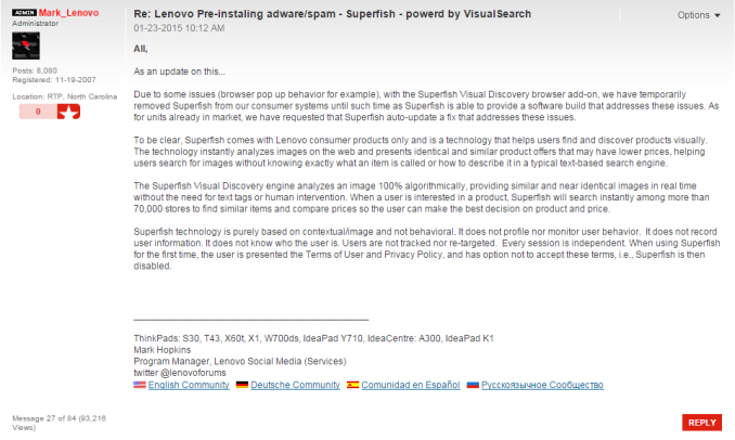
The reason this situation has come to the forefront today is due to a tweet on Wednesday by the co-director of the Open Crypto Audit Project and a single forum post by a Lenovo employee, describing how SuperFish works:
Despite whatever good intentions Lenovo had behind the software, the implementation as well as the execution leave a lot to be desired, especially in a climate where security and privacy are key factors with their main user demographic. I doubt that any such software would ever been considered in this digital age as viable, unless it was forced upon a user at a work machine to only ever be used for that purpose. But for home users, this post waves a black flag followed by a red one – the race is being stopped and you are being disqualified.
There are two elements to this story from Lenovo. Perhaps understandably, the forum post mentions that SuperFish is currently disabled on Lenovo’s end. However, the software is still active on the user machines and can still issue weak security certificates while the user-side software tries to analyze website images.
The next is an official response on SuperFish, which you can read here. A brief summary is included here:
- SuperFish was previously included in some consumer notebooks shipped between September and December 2014.
- User Feedback was not positive.
- SuperFish has been disabled server-side since January.
- Lenovo stopped preloading the software in January.
- Lenovo will not preload this software in the future.
- Lenovo is providing support on its forums for any user with concerns. If users still wish to take further action, detailed information is available here.
As noted, the response from the community about SuperFish has been negative. Marc Rogers writes a particularly scathing post about the situation, and mainstream media such as the BBC is actively picking up on the issue. Over 30 models are affected by this software, all of which are noted in the official Lenovo response, and details are provided on how to remove the software. If you think you are affected, @FiloSottile is hosting a SuperFish detector at https://filippo.io/Badfish/. There are also extra instructions to remove malicious certificates from a system at the bottom of the page here.
Lenovo has stated that new units are no longer preloaded with SuperFish. However, there are most likely units still in the supply chain from before January that have the software. Lenovo is issuing an update to SuperFish to disable itself if the user accepts the user agreement on first use.
The end result is that this comes at the expense of Lenovo’s reputation. As a brand that has made it into most of the largest markets around the world, there’s an element of trust that takes years to build and a single action to erode. I suspect there will be some calls for investigations or forms of compensation, and at this point it is difficult to estimate if any legal action will be sought or anything illegal can be proven due to compromised systems. Lenovo at this time is treading carefully, only providing an official statement on the issue despite the initial furor caused over a single forum post that has now been viewed over 100,000 times.
I’m sitting at my work desk with a Core-M based Yoga 3 Pro and fortunately it is not one of the models affected. Loading up a detection website confirms this. Normally on AnandTech our testing is directed mostly at the hardware, the performance and the design choices made, but rarely the politics. It is a difficult subject for a website like AnandTech to tackle, and given the amount of information around, it is important to stick to the facts here. There has already been a backlash over social media about SuperFish, and Lenovo has acted quickly. Some users will be expecting an apology, rather than the attempted justification, and we will have to see how this situation develops. I can imagine Lenovo not stating anything except through official channels for a while. They will be presenting and have a booth at Mobile World Congress in March, so we may (or may not) see any development then.
Sources: Lenovo, Marc Rogers, Errata Security, @FiloSottile
More...
-
02-20-15, 08:02 AM #4754
Anandtech: Intel NUC5i5RYK Review: A Broadwell-U UCFF PC for Enthusiasts
The Intel NUC category has been an interesting product line to analyze, as it provides us with insights into where the traditional casual / home use desktop market might end up. UCFF (ultra-compact form factor) PCs have had an excellent reception in the market, both from home and business users. Intel kickstarted the market with the Sandy Bridge NUCs a couple of years back. Since then, we have had NUCs based on Ivy Bridge, Haswell and even Bay Trail. Today, we will take a look at what Intel has brought to the table with Broadwell.
More...
-
02-20-15, 08:02 AM #4755
Anandtech: Apple Initiates Video Repair Program for 2011-2013 MacBook Pros
This week Apple has announced that they are initiating a new repair extension program for the MacBook Pro, in order to address video corruption and stability problems with certain models. The program offers extended repair service for the 15” and 17” 2011 MacBook Pros, along with the 2012 and Early 2013 15” Retina MacBook Pros.
Under the terms of the program, covered laptops that are experiencing video issues such as display corruption, system crashes, or other glitches will be eligible for free repairs through Apple. Furthermore all affected systems are eligible regardless of warranty status, making this a true extension in every sense of the word as the bulk of the systems this program covers are past their extended warranty expiration dates. Meanwhile in order to compensate any users who have already suffered from the issue, Apple is also offering reimbursements to those customers who have already paid for repairs.
The MacBook Pro repair program comes less than 2 years after Apple’s last repair program, which in 2013 saw Apple offering free video card replacements and repairs for the mid-2011 27” iMac. And given the similarities between the problems in the MacBook Pro and the iMac, this has raised a few eyebrows. While the 2011 iMac and MacBook Pros use different GPUs, both systems use GPUs from AMD’s Radeon HD 6000M series, with the iMac using the higher-end 6970M while the MacBook Pros used the 6490M, 6750M, and 6770M GPUs.
However throwing a wrench into any common thread between these systems, the last of the MacBook Pros covered by the repair program, the first generation 15” Retina MacBook Pros, used NVIDIA’s GeForce GT 650M instead. There is also the matter of differences in construction – iMacs used MXM cards, MacBook Pros use GPUs soldered on to the logic board – and even differences in operation. Namely, while the iMac used its dGPU exclusively the MacBook Pros all used switchable graphics, which means that the MacBook Pros are often being driven by their iGPU rather than their dGPU.
Consequently while we first suspected that this is a common issue revolving around the Radeon HD 6000M series – and certainly we can’t rule that out – there seems to be more that’s going on here than a common failure in one line of GPUs. This could include Apple opting to address multiple modes of failure under a single repair program, or even just pure coincidence. At the same time we haven’t seen a widespread repair program issued by other OEMs for any of these GPUs, which may mean that Apple is the only OEM being seriously affected, unlike NVIDIA’s bumpgate which saw repair programs from a number of OEMs.
For that reason I find myself wondering whether another factor such as cooling has been playing a role here. Although these Apple devices all use different coolers, one common element in Apple’s iMac and Retina MacBook Pro designs has been the comapny's aggressiveness in controlling the thickness of those devices, leading to them pushing the envelope on cooling relatively high TDP processors in tight spaces.
In any case, the full details of the program, including the affected models and repair instructions, are available over at Apple’s website.
More...
-
02-20-15, 02:00 PM #4756
Anandtech: NVIDIA Mobile Overclocking - There and Back Again
The past few months have been a bit interesting on the mobile side of the fence for NVIDIA. Starting with the R346 drivers (347.09 beta and later), NVIDIA apparently decided to lock down overclocking of their mobile GPUs. While this is basically a non-issue for the vast majority of users, for the vocal minority of enthusiasts the reaction has been understandably harsh. Accusations have ranged from “bait and switch” (e.g. selling a laptop GPU that could be overclocked and then removing that “feature”) to “this is what happens when there’s no competition”, and everything in between.
NVIDIA for their part has had a few questionable posts as well, at one point stating that overclocking was just “a bug introduced into our drivers” – a bug that has apparently been around for how many years now? And with a 135MHz overclocking limit no less…. But there’s light at the end of the tunnel, as NVIDIA has now posted that they will be re-enabling overclocking with their next driver update, due in March. So that’s the brief history, but let’s talk about a few other aspects of what all of this means.
First and foremost, anyone that claims enabling/disabling overclocking of mobile GPUs is going to have a huge impact on NVIDIA’s bottom line is, in my view, spouting hyperbole and trying to create a lot of drama. I understand there are people that want this feature, and that’s fine, but for every person that looks at overclocking a mobile GPU there are going to be 100 more (1000 more?) that never give overclocking a first thought, let alone a second one. And for many of those people, disabling overclocking entirely isn't really a bad idea – a way to protect the user from themselves, basically. I also don’t think that removing overclocking was ever done due to the lack of competition, though it might have had a small role to play. At most, I think NVIDIA might have disabled overclocking because it’s a way to keep people from effectively turning a GTX 780M into a GTX 880M, or the current GTX 980M into a… GTX 1080M (or whatever they call the next version).
NVIDIA’s story carries plenty of weight with me, as I’ve been reviewing and helping people with laptops for over a decade. Their initial comment was, “Overclocking is by no means a trivial feature, and depends on thoughtful design of thermal, electrical, and other considerations. By overclocking a notebook, a user risks serious damage to the system that could result in non-functional systems, reduced notebook life, or many other effects.” This is absolutely true, and I’ve seen plenty of laptops where the GPU has failed after 2-3 years of use, and that’s without overclocking. I've also seen a few GTX 780M notebooks where running at stock speeds isn't 100% stable, especially for prolonged periods of time. Sometimes it’s possible to fix the problem; many people simply end up buying a new laptop and moving on, disgruntled at the OEM for building a shoddy notebook.
For users taking something like a Razer Blade and trying to overclock the GPU, I also think pushing the limits of the hardware beyond what the OEM certified is just asking for trouble. Gaming GPUs and “thin and light” are generally at opposite ends of the laptop spectrum, and in our experience the laptops can already get pretty toasty while gaming. So if you have a laptop that is already nearing the throttling point, overclocking the GPU is going to increase the potential of throttling or potentially even damage the hardware. Again, I’ve seen enough failed laptops that there’s definitely an element of risk – many laptops seem to struggle to run reliably for more than 2-3 years under frequent gaming workloads, so increasing the cooling demands is just going to exacerbate the problem.
On the other hand, if you have a large gaming notebook with a lot of cooling potential and the system generally runs cool, sure, it’s nice to be able to push the hardware a bit further if you want. We don’t normally investigate overclocking potential on notebooks as it can vary between units of the same family, and in many cases it voids the warranty, but enthusiasts are a breed apart. My personal opinion is that for a gaming laptop, you should try to keep GPU temperatures under 85C to be safe (which is what most OEMs tend to target); when laptops exceed that “safe zone” (with or without overclocking), I worry about the long-term reliability prospects. If you have a GPU that’s running at 70C under load, however, you can probably reliably run the clocks at the maximum +135MHz that NVIDIA allows.
We’re currently in the process of testing a couple of gaming notebooks, and given the timing of this we’re going to use this as an opportunity to try some overclocking – with the older 344.75 drivers for now. We’ll have a separate article digging into the overclocking results later, but again I’d urge users to err on the side of caution rather than trying to redline your mobile GPU. What that means in practice is that mobile GPU overclocking is mostly going to be of use for people with larger gaming notebooks – generally the high-end Alienware, ASUS, Clevo, and MSI models. There may be other laptops where you can squeeze out some extra performance (e.g. some models with GTX 850M/860M, or maybe even some older GT 750M laptops), but keep an eye on the thermals if you want to go that route.
More...
-
02-20-15, 06:00 PM #4757
Anandtech: Samsung Releases Statement on 840 EVO Performance - Another Fix Is In the
Over the last month there has been some concern over the read performance of Samsung’s 840 EVO drives, and whether after Samsung’s previous performance fix, that these same drivers are starting to regress in performance once again. Since then we have been pressuring Samsung for additional information on the issue and a response, and this afternoon Samsung has finally issued a statement on the matter.
In October, Samsung released a tool to address a slowdown in 840 EVO Sequential Read speeds reported by a small number of users after not using their drive for an extended period of time. This tool effectively and immediately returned the drive’s performance to normal levels. We understand that some users are experiencing the slowdown again. While we continue to look into the issue, Samsung will release an updated version of the Samsung SSD Magician software in March that will include a performance restoration tool.As a reminder, the original 840 EVO performance degradation issue was a result of a combination of NAND cell charge decay and NAND management algorithm issues. While NAND cell charge decay is a normal part of NAND operation, it was something Samsung’s more complex TLC NAND was more sensitive to. Meanwhile Samsung’s algorithms, when faced with this decay, erroneously went into an aggressive read-retry state, which is ultimately what lead to the drop in read performance. Samsung’s fix in turn addressed their NAND management algorithm, and at least at the time was thought to be a permanent fix for the issue.
These more recent performance issues and now Samsung’s statement make it clear that the issue is unfortunately not as fixed as Samsung initially thought it would be. At this point Samsung isn’t saying what the root cause of this latest issue is, but it’s likely that this is a continuation of the original issue. In any case the upshot is that Samsung believes the issue can be corrected, however given the last fix it’s not clear whether this next fix will be any more a permanent fix than the last one.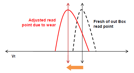
More...
-
02-22-15, 03:00 PM #4758
Anandtech: Intel at ISSCC 2015: Reaping the Benefits of 14nm and Going Beyond 10nm
As part of the International Solid-State Circuits Conference every year, Intel brings forward a number of presentations regarding its internal research. The theme this year at ISSCC is ‘Silicon Systems – Small Chips for Big Data’, and Intel previewed a number of their presentations with the media and analysts last week before the conference. Hot topics being talked about include developments for 14nm features that could potentially be ported to real world devices, technological developments at 22nm using Tri-Gate CMOS for adaptive, autonomous and resilient systems and also a few quick words regarding 10nm and beyond.
Taking Moore’s Law Beyond 10nm
Part of ISSCC will be a round table with representatives from Intel, Qualcomm, a couple of industry companies and university researches discussing how 10nm will attack Moore’s Law and how it can be extended below to 7nm. The graphs shown at IDF 2014 make their presence again, showing cost per square mm and cost per transistor, courtesy of Mark Bohr (Intel Senior Fellow, Logic Technology Development):
The fact that 14nm resulted in a better-than-the-trend drop in cost per transistor was explained as some internal smart reworking, making sure that certain areas of the dies require different masking and by optimizing the masking process, the cost can be reduced rather than relying on fewer general masks (but it is still a balance).
It was explained that while 10nm will have more masking steps than 14nm, and the delays that bogged down 14nm coming late to market will not be present at 10nm – or at least reduced. We were told that Intel has learned that the increase in development complexity of 14nm required more internal testing stages and masking implementations was a major reason for the delay, as well as requiring sufficient yields to go ahead with the launch. As a result, Intel is improving the efficiency testing at each stage and expediting the transfer of wafers with their testing protocols in order to avoid delays. We were quoted that 10nm should be 50% faster to market than 14nm was as a result of these adjustments. So while the additional masking steps at 10nm which ultimately increases fixed costs, Intel is still quoting that their methods results in a reducing in terms of cost per transistor without needing a completely new patterning process. EUV lithography was discussed, but Intel seems to be hoping to avoid it until it is absolutely necessary, as EUV development so far has been slower to progress than expected.
10 nm will come with innovation, and getting down to 7 nm will require new materials and processes which Intel wants to promote as a progressive integration between process development and the product design teams. New materials and device structures are key elements on that list, and while III-V materials were discussed in the ISSCC preview, no exact details were given.
Hot on the lips regarding Moore’s Law challenges comes down to future integrated systems, specifically 2.5D (separate dies on an interposer) and 3D (stacked dies). While 2.5D and 3D are not direct replacements for Moore’s Law due to the increase in cost per transistor overall, it is being examined in terms of high power usages (2.5D) or size-limited integrated topologies (3D). Specifically, Intel is looking at scenarios where logic blocks using different fabrication methods are laid out in their own layers and stacked, rather than implemented on a single layer of a single die (think memory, digital logic, and analog communications on a single chip). This kind of a configuration may appear in smartphones, tablets or devices that use other highly-integrated logic where multiple types of fabrication would be necessary and a premium price can be applied. We have discussed in the past how 2.5D and 3D configurations can improve performance, especially when it comes to memory density and graphics bandwidth, however the price increase (according to Intel) will result in that premium, even at high volume.
Reaping the Benefits of 14nm
Intel is highlighting a trio of papers at ISSCC regarding 14nm. One of the areas ripe for exploitation at 14nm is data transfer, especially transmitters. To that extent, Intel is showing a 14nm Tri-Gate CMOS serializer/deserializer transmitter capable of 16-40 Gbps, using both the NRZ (non-return zero) and PAM4 (Pulse-Amplitude Modulation with 4 levels) modes within a 0.03 millimeter squared die area.
Also on data transfer is a paper regarding the lowest power 10Gb/s serial link and the first complete serial link using 14nm Tri-Gate CMOS. Intel has working silicon at 14nm showing a 59mW power consumption within 0.065 millimeters squared die area that configures the committed data rate to provide the cleanest data response.
Perhaps the most exciting 14nm development is in the form of memory, with Intel describing in-house 84Mb SRAM design that uses the world’s smallest bitcell (0.050 micron squared). At 14nm it represents a doubling of the density at 14.5 Mb per square millimeter, but also provides substantially lower minimum voltage for a given frequency compared to the previous 22nm process. As shown in the graph in the slide, 0.6V is good for 1.5 GHz, but it can scale up to 3 GHz. It is also worth noting that the 14nm yield gradient is more conducive to lower voltage operation compared to the 22nm process. While it seems odd to promote an 84Mb (10.5 MB) design, Intel discussed that it can be scaled up over 100 Mb or more, making it a better solution for embedded devices rather than something like Crystal Well on desktop.
Still Developing on 22nm
While 14nm is great for density, lower voltage and lower power, other features on die are often produced at a looser resolution in order to ensure compatibility but it also offers a great research platform for testing new on-die features to be scaled down at a later date. To this extent, Intel Labs is also presenting a couple of papers about in-house test chips for new features.
The first test chip concerns data retention within register files. Depending on the external circumstances such as temperature and age, this adaptive and resilient domino register file testchip is designed to realign timing margins and detect errors as they occur and adjust the behavior in order to compensate. The logic that Intel is presenting is designed to also cater for die variation and voltage droop, making it more of a universal solution. On a higher level it sounds like the situation when NAND flash gets old and the onboard controller has to compensate for the voltage level margins.
The second test-chip being described brings the situation down to Intel’s execution units in its graphics and dealing with fast, autonomous and independent dynamic voltage scaling. The use of a combined low-dropout regulator (LDO) for low voltages, such as at idle, and a switched capacitor voltage regulator (SCVR) for high voltages allow the appropriate current injection to deal with voltage droop as well as resulting in a large energy reduction. When applied, this should allow for either a power drop at the same frequency, or a higher frequency at the same voltage. Currently the numbers provided by Intel are all on internal silicon rather than anything in the wild, and will be examined at smaller nodes in due course.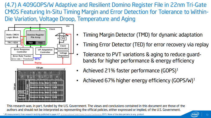
Intel at ISSCC
ISSCC always throws out some interesting information about what is actually going on under the hood with the silicon we use almost every day, as we tend to think about it as a black box that slowly gets better over time. In reality, new features are fully researched and documented in order to be included in the next model, as well as trying to keep a balance of power usage and efficiency. On the CPU architecture side of the equation, we reported that Broadwell features needed to show a 2% performance or efficiency improvement for every 1% increase in power, making that advancement steeper than the 1:1 previously required. For all intents and purposes this means that if the same strategy is applied to 10nm and beyond, we are in for a very interesting time. It was interesting to hear about Intel speeding up on 10nm to avoid the delays occurred at 14nm, as well as thoughts regarding future technologies.
The papers Intel is presenting should be available via the ISSCC website as the presentations take place, along with a few others that pique our interest. This should get us ready for some interesting developments come Intel's Developer Forum later in the year.
More...
-
02-23-15, 03:01 PM #4759
Anandtech: Cougar 700K Mechanical Keyboard & 700M Gaming Mouse Review
Cougar was founded in Germany over seven years ago, with an initial focus on computer power supplies and cases. More recently, the company has diversified into the gaming peripherals market and today we have a combo review of the 700K and the 700M, their best mechanical keyboard and gaming mouse, respectively. We all know that this market segment is saturated, so what new do these products bring? Read on to find out.
More...
-
02-23-15, 04:00 PM #4760
Anandtech: Google Acquires Softcard and Partners with US Carriers On Mobile Payments
Today Google has acquired the technology and IP behind Softcard. Softcard is a joint venture between AT&T, Verizon, and T-Mobile to support NFC based mobile payments in the United States. While Google's original post on the Google Commerce blog described it as something closer to a partnership, the statement released by Softcard confirms that Google has purchased Softcard's technology.
According to the statement released by Google, they have partnered with the three major US carriers that created the Softcard payment platform to increase the adoption and availability of Google Wallet, which is Google's mobile payment platform that launched in 2011. Under this new partnership, Android devices sold by those carriers that are running KitKat or newer will come with the Google Wallet application pre-installed.
This cooperation between Google and the US carriers is a surprising development. In the past, the competition between Softcard and Google Wallet led to situations like Google Wallet being disabled on the Verizon Galaxy Nexus. It will be interesting to see how the expansion of mobile payments plays out with both Google and the major US carriers putting their weight behind one standard.
Source: Softcard and Google
More...


 Quote
Quote

Thread Information
Users Browsing this Thread
There are currently 24 users browsing this thread. (0 members and 24 guests)


Bookmarks