

Results 4,981 to 4,990 of 12091
Thread: Anandtech News
-
05-07-15, 10:30 PM #4981
Anandtech: NVIDIA Announces FY 2016 Q1 Financial Results
Today NVIDIA released their earnings for quarter one of their 2016 fiscal year (and no, that’s not a typo, NVIDIA is almost a full calendar year ahead with their fiscal year) and revenue was up for the quarter 4% over the same period last year, coming in at $1.151 billion. NVIDIA had a record quarter for gross margin, with 56.7% this quarter. However net income was down 2% to $134 million. Compared to Q4 2015, revenue was down 8% and net income was down 31% due to the seasonal nature of the GPU market. Earnings per share came in at $0.24, which is flat year-over-year.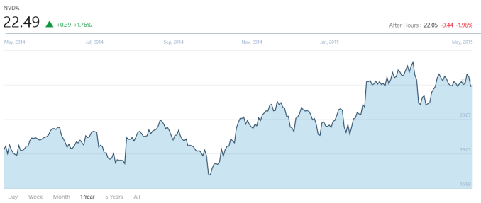
One of the things that will be impacting their financials for fiscal year 2016 is the winding down of the Icera modem operations. The company is open to sales, but regardless it is expecting restructuring charges of $100 to $125 million. It will re-invest the money it had been using for modems and put it into deep learning, self-driving cars, and gaming, which are all areas where NVIDIA has seen some success at (I’ve heard they are known for gaming even).NVIDIA Q1 2016 Financial Results (GAAP) Q1'2016 Q4'2015 Q1'2015 Q/Q Y/Y Revenue (in millions USD) $1151 $1251 $1103 -8% +4% Gross Margin 56.7% 55.9% 54.8% +0.8% +1.9% Operating Expenses (in millions USD) $477 $468 $453 +2% +5% Net Income $134 $193 $137 -31% -2% EPS $0.24 $0.35 $0.24 -31% flat
NVIDIA has also announced Non-GAAP results which exclude stock-based compensation, acquisition costs, interest, and taxes on these items. On a Non-GAAP basis, gross margin was 56.9%, and net income was $187 million, which is up 13% year-over-year. Non-GAAP earnings per share came in at $0.33.
Breaking the results down into the individual segments, the GPU unit accounts for the bulk of the revenue for the company. GPU revenues were up 5% year-over-year, coming in at $940 million for Q1. They attribute this to revenue from GeForce gaming desktops and notebooks growing 14% with strength in their Maxwell GPUs being one of the keys. Notebooks have also been a source of strength, and although they did not release numbers, notebook GPU sales were “well above year-ago levels”. Tesla GPUs also increase due to project wins with cloud service providers, but the Quadro line of professional graphics declined.NVIDIA Q1 2016 Financial Results (Non-GAAP) Q1'2016 Q4'2015 Q1'2015 Q/Q Y/Y Revenue (in millions USD) $1151 $1251 $1103 -8% +4% Gross Margin 56.9% 56.2% 55.1% +0.7% +1.8% Operating Expenses (in millions USD) $425 $420 $411 +1% +3% Net Income $187 $241 $166 -22% +13% EPS $0.33 $0.43 $0.29 -23% +14%
Tegra, once the tablet and possible smartphone SoC, has found its niche is the automotive infotainment field, but it is also the SoC inside SHIELD devices sold by NVIDIA. Revenue for Tegra was up 4% year-over-year, and up 29% as compared to Q4 2015, which was attributed to automotive systems and development services.NVIDIA Quarterly Revenue Comparison (GAAP) In millions Q1'2016 Q4'2015 Q1'2015 Q/Q Y/Y GPU $940 $1073 $898 -12% +5% Tegra Processor $145 $112 $139 +29% +4% Other $66 $66 $66 flat flat
The final piece of NVIDIA’s pie is their licensing agreement with Intel, which is the standard $66 million per quarter.
For Q2, projections are revenue of $1.01 billion, plus or minus two percent, and gross margins of 55.7% plus or minus 0.5%.
It was another good quarter for NVIDIA, and during the quarter they launched the TITAN X GPU, as well as the NVIDIA SHIELD set top box. Yesterday, AMD announced that they will have a new GPU coming out this quarter, so it will be awesome to see how that plays out in the never ending GPU battle.
Source: NVIDIA Investor Relations
More...
-
05-08-15, 07:05 AM #4982
Anandtech: The Intel Xeon E7-8800 v3 Review: The POWER8 Killer?
The story behind the High-end Xeon has been the same for the past 5 years: Intel's most expensive beats the Oracle alternative in every way you can look at it, and offers better performance per watt/dollar than the massive IBM Power servers. And each time a new generation of quad/octal socket Xeons is born, Intel increases the corecount, RAS features and performance per core while charging a lot more for the top SKUs. From the Intel side, this new generation is no different: more cores, better RAS, slightly more performance per core and ... higher prices.
More...
-
05-08-15, 07:30 PM #4983
Anandtech: Rightware's Benchmark Division Acquired By Basemark
Yesterday, Rightware founder Tero Sarkkinen aquired Rightware's benchmarking unit and made it part of his newly founded company, Basemark Ltd. Sarkkinen founded Rightware as well five years ago, making this subsequent purchase a spin-off of sorts that sees the Basemark division being recreated as its own company.
Rightware's benchmarks such as Basemark OS II and Basemark X are ones that we use in many of our reviews. Today's deal is more like Rightware's benchmarking division separating into a new company rather than them being acquired. All of the Rightware benchmarking division's existing technologies, licenses, and commercial contracts have been transferred to the new company as part of the deal. More info about the new independent Basemark Ltd and their benchmarks can be found in the link below.
More...
-
05-11-15, 07:42 AM #4984
Anandtech: Interacting with HTPCs: Logitech and Perixx Options Reviewed
We have reviewed a number of HTPC keyboards from vendors such as IOGEAR, SIIG and Adesso in our 'Interacting with HTPCs' series. All of them were compared with the Logitech K400 - one of the most popular options in this space due to the combination of its feature set and pricing. What happens when one searches for units that go deep on either side of that in the pricing spectrum? Read on for our review of a couple of options each from Perixx and Logitech.
More...
-
05-12-15, 03:36 AM #4985
Anandtech: MediaTek Unveils Helio X20 Tri-Cluster 10-Core SoC
Today MediaTek announces their brand new flagship SoC for smartphones and tablets, the Helio X20. MediaTek continues their Helio SoC branding announced earlier in the year, making the X20 the second SoC in the X-lineup and the first one to be actually released with the new product name from the beginning (as the X10 was a direct name change from the MT6795).
Right off the bat, MediaTek manages to raise eyebrows with what is the first 10 core System-on-a-Chip design. The 10 processors are arranged in a tri-cluster orientation, which is a new facet against a myriad of dual-cluster big.LITTLE heterogeneous CPU designs. The three clusters consist of a low power quad-core A53 cluster clocked at 1.4 GHz, a power/performance balanced quad-core A53 cluster at 2.0GHz, and an extreme performance dual-core A72 cluster clocked in at 2.5GHz. To achieve this tri-cluster design, MediaTek choose to employ a custom interconnect IP called the MediaTek Coherent System Interconnect (MCSI).
We'll get back to the new innovative CPU arrangement in a bit, but first let's see an overview of what the rest of SoC offers. MediaTek is proud to present its first CDMA2000 compatible integrated modem with the X20. This is an important stepping stone as the company attempts to enter the US market and try to breach Qualcomm's stronghold on the North American modems and SoCs. Besides C2K, the X20's modem allows for LTE Release 11 Category 6 with 20+20MHz Carrier Aggregation (downstream), supporting speeds up to 300Mbps in the downstream direction and 50Mbps upstream. The new modem also is supposed to use 30% less power when compared to the Helio X10.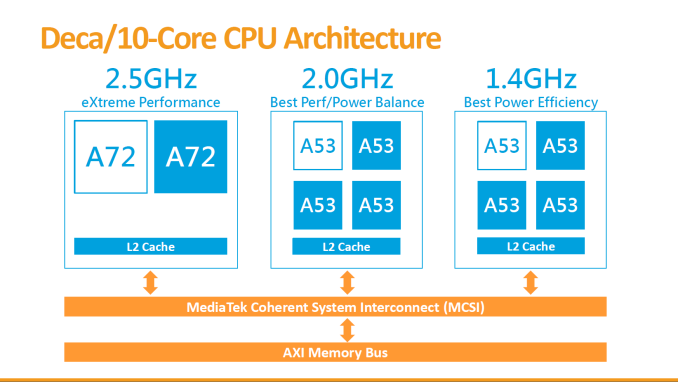
The SoC also has an integrated 802.11ac Wi-Fi with what seems to be a single spatial stream rated in the spec sheets up to 280Mbps.
Video encoding and decoding capabilities seem to be carried over from the MT6795 / X10, but MediaTek advertises a 30% and 40% improvement in decoding and encoding power consumption respectively.MediaTek Helio X20 vs The Competition SoC MediaTek
Helio X20
(MT6797)MediaTek
Helio X10
(MT6795)Qualcomm
Snapdragon 808
(MSM8992)Qualcomm
Snapdragon 620
(MSM8976)CPU 4x Cortex A53 @1.4GHz
4x Cortex A53 @2.0GHz
2x Cortex A72
@2.3-2.5GHz4x Cortex A53 @2.2GHz
4x Cortex A53 @2.2GHz4x Cortex A53 @1.44GHz
2x Cortex A57 @1.82GHz4x Cortex A53 @1.2GHz
4x Cortex A72 @1.8GHzMemory
Controller2x 32-bit @ 933MHz
LPDDR3
14.9GB/s b/w2x 32-bit @ 933MHz
LPDDR3
14.9GB/s b/w2x 32-bit @ 933MHz
LPDDR3
14.9GB/s b/w2x 32-bit @ 933MHz
LPDDR3
14.9GB/s b/wGPU Mali T8??MP4
@700MHzPowerVR G6200
@700MHzAdreno 418
@600MHz"Next-gen" Adreno Encode/
Decode2160p30 10-bit
H.264/HEVC/VP9
decode
2160p30
HEVC w/HDR
encode2160p30 10-bit
H.264/HEVC/VP9
decode
2160p30
HEVC
encode2160p30, 1080p120
H.264 & HEVC
decode
2160p30, 1080p120
H.264
encode2160p30, 1080p120
H.264 & HEVCCamera/ISP Dual ISP
32MP @ 24fps13MP Dual ISP
21MPDual ISP
21MPIntegrated
ModemLTE Cat. 6
300Mbps DL 50Mbps UL
2x20MHz C.A.
(DL)LTE Cat. 4
150Mbps DL 50Mbps UL"X10 LTE" Cat. 9
450Mbps DL
50Mbps UL
3x20MHz C.A.
(DL)"X8 LTE" Cat. 7
300Mbps DL 100Mbps UL
2x20MHz C.A.
(DL & UL)
Still on the multimedia side, we see the employment of a new integrated Cortex-M4 companion-core which serves as both an audio processor for low-power audio decoding, speech enhancement features and voice recognition, as well as sensor-hub function acting as a microcontroller for offloading sensor data processing from the main CPU cores. This means that while the device has the display turned off but is playing audio, only the M4 is in use in order to decrease battery life.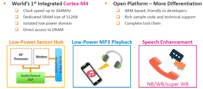
On the GPU side, the X20 seemed to be the first officially announced Mali T800 series GPU SoC. MediaTek explains that this is a still-unreleased ARM Mali high-end GPU similar to the T880. MediaTek initially choose a more conservative MP4 configuration clocked in at 700MHz, although final specifications are being withheld at this time. It should be noted that Mediatek has traditionally never aimed very high in terms of GPU configurations. It could be considered that the GPU in the X20 could still remain competitive in prolonged sustained loads as we saw larger Mali implementations such as Samsung's Exynos SoCs not being able to remain in the thermal envelope at their maximum rated frequencies. Initial relative estimates of the X20, expressed by MediaTek, compared to the Helio X10's G6200 see a 40% improvement in performance with a 40% drop in power.
On the memory side, MediaTek remains with a 2x32bit LPDDR3 memory interface running at 933MHz. MediaTek reasons that the SoC is limited to 1440p devices and the LPDDR3 memory should be plenty enough to satisfy the SoC's bandwidth requirements (a notion I agree with, given the GPU configuration).
Going back to the signature 10-Core/Tri-Cluster architecture of the SoC, MediaTek explains that this was a choice of power optimization over conventional two-cluster big.LITTLE designs. b.L works by employing heterogeneous CPU clusters - these may differ in architecture, but can also be identical architectures which then differ in their electrical characteristics and their target operating speeds. We've covered how power consumption curves behave in our Exynos 5433 deep-dive, and MediaTek presents a similar overview when explaining the X20's architecture.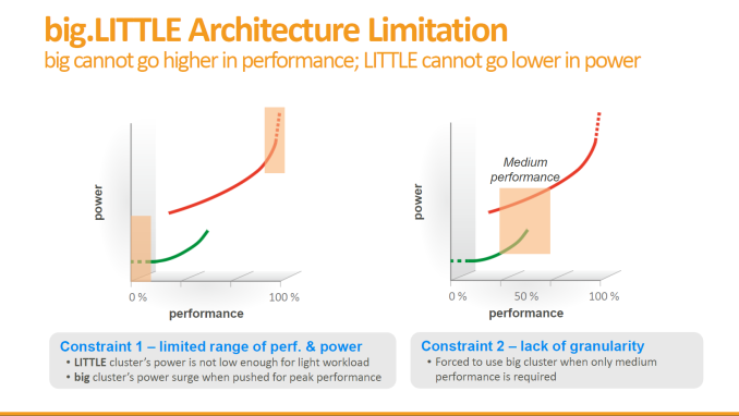
One option in the traditional 2-cluster designs is to employ a low-power low-performance cluster, typically always a lower-power in-order CPU architecture such as ARM's A53. This is paired with a higher-power high-performance cluster, either a larger CPU core such as the A57/A72, or a frequency optimized A53 as we see employed in some past MediaTek SoCs, or most recently, HiSilicon's Kirin 930 found in the Huawei P8.
Contrary to what MediaTek presents as an "introduction of a Mid cluster", I like to see MediaTek's tri-cluster approach as an extension to the existing dual A53 cluster designs - where the added A72 cluster is truly optimized for only the highest frequencies. Indeed, we are told that the A72 cluster can reach up to 2.5GHz on a TSMC 20nm process. ARM aims similar clocks for the A72 but at only 14/16nm FinFET processes, so to see MediaTek go this high on 20nm is impressive, even if it's only a two-core cluster. It will be interesting to see how MediaTek chooses the lower frequency limits on each cluster, especially the A72 CPUs, or how these options will be presented to OEMs.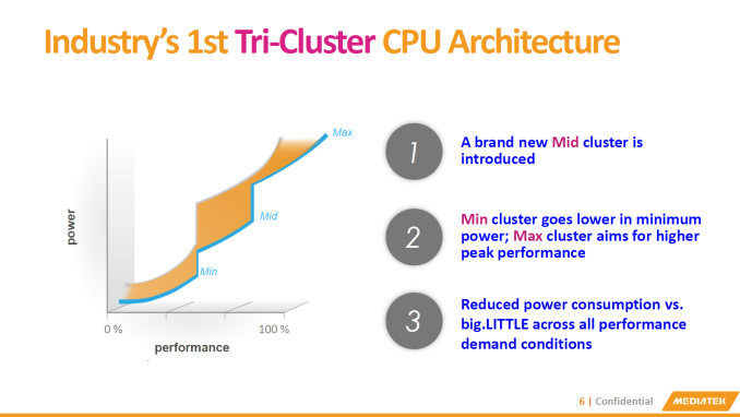
The end-result is a promised 30% improvement in power consumption over a similar 2-cluster approach. This happens thanks to the finer granularity in the performance/power curve and an increase in available performance-power points for the scheduler to place a thread on. Having a process that is heavy enough that it is not capable of residing on the smallest cluster due to performance constraints, but not demanding enough to require the big cluster's full performance, can now reside on this medium cluster at much greater efficiency than had it been running on the big cluster at reduced clocks. MediaTek uses CorePilot as a custom developed scheduler implementation that is both power aware and very advanced (based on our internal testing of other MediaTek SoCs). My experience and research with it on existing devices was fairly positive, so I'm sure the X20's new v3.0 implementation of CorePilot will be able to take good advantage of the tri-cluster design.
The biggest question and need of clarification is in the area of what the MCSI (the interconnect) is capable of. ARM had announced its CCI-500 interconnect back in February, which incidentally also promised the capability of up to 4 CPU clusters. MediaTek hinted that this may be a design based on ARM's CCI - but we're still not sure if this means a loosely based design or a direct improvement of ARM's IP. Cache coherence is a major design effort, and if MediaTek saw this custom IP as an effort worth committing to, then the MCSI may have some improvements we're still not clear on.
The Helio X20 is certainly an interesting SoC and I'm eager on how the tri-cluster design performs in practice. The X20 samples in H2 2015 and devices with it are planned to be shipping in Q1 2016. In the given time-frame, it seems the X20's primary competitor is Qualcomm's Snapdragon 620, so it'll be definitely a battle for the "super-mid" (as MediaTek likes to put it) crown.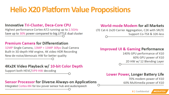
More...
-
05-12-15, 04:38 AM #4986
Anandtech: AMDs Carrizo-L APUs Unveiled: 12-25W Quad Core Puma+
One of the important press releases that came out as a result of the AMD Financial Analyst Day has been some insights into how AMD is approaching the Carrizo and Carrizo-L platform. Have a read of Ryan’s round up of the Financial Analyst Day, which included some broad details about Zen and the big x86 cores, but Carrizo and Carrizo-L focus on AMD’s mobile strategy as well as describing the next iterations of the Bulldozer architecture (Excavator) and the Cat family of low power SoCs (Puma+). We covered some of AMD’s releases on Carrizo back in February, but despite the similar name Carrizo-L functions for a slightly different market by virtue of the different architecture.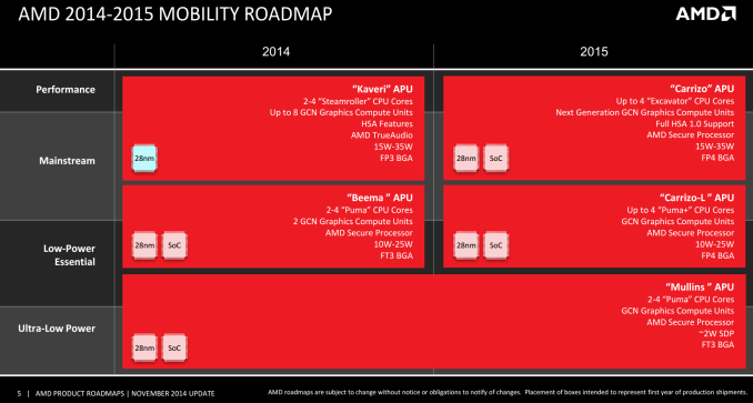
Carrizo-L features ‘Puma+’, which by virtue of the naming scheme suggests an updated version of Puma which was seen in Beema. What the ‘plus’ part of the name means has not been disclosed, as both Puma and Puma+ are reported to be 28nm, but chances are that the design has attacked the low hanging fruit in the processor design, rather than purely just a frequency bump. Carrizo-L will be advertised under the new ‘AMD 7000 Series’ APUs, featuring up to four low power separate cores up to 2.5GHz, up to 25W and up to DDR3-1866 support. These are aimed square at the Atom ecosystem within a similar power budget.
AMD is stating that these APUs are currently available in Greater China already with a global rollout commencing in due course. All APUs are listed with AMD Radeon graphics, although the Rx number has no indication as to the streaming processors in the graphics part – a similar situation happened with Beema, and all those parts came with 128 SPs, differing only in frequency which is likely the case here. The SoC design also ensures all the IO is onboard, including an AMD Secure Processor, which for Puma was a Cortex-A5 supporting ARM TrustZone. It is likely that Carrizo-L also uses only a single memory channel, similar to Beema.AMD Carrizo-L A8-7410 A6-7310 A4-7210 E2-7110 E1-7010 Cores / Threads 4 / 4 4 / 4 4 / 4 4 / 4 2 / 2 CPU Frequency Up to 2.5 GHz Up to 2.4 GHz Up to 2.2 GHz Up to 1.8 GHz Up to 1.5 GHz TDP 12-25W 12-25W 12-25W 12-15W 10W L2 Cache 2MB 2MB 2MB 2MB 1MB DRAM Frequency DDR3L-1866 DDR3L-1600 DDR3L-1600 DDR3L-1600 DDR3L-1333 Radeon Graphics R5 R4 R3 'Radeon' 'Radeon' Streaming Processors 128 ? 128 ? 128 ? 128 ? 128 ? GPU Frequency Unknown Unknown Unknown Unknown Unknown
One of the more interesting elements is that Carrizo and Carrizo-L will share a socket, known as FP4. This means the processors are pin compatible, and what we know about Carrizo at this point suggests that both segments will play within the same sort of power budget (10-25W vs 15-35W). This allows OEMs to build two designs with almost identical hardware under the hood except for the SoC – would you prefer a single/dual Excavator design, or a faster frequency quad-core Puma+ design? There also leaves scope for differential integrated graphics performance, as mobile Kaveri up to 25W had up to 384 SPs or 3x what we are expecting with Carrizo-L. A lot of the performance metrics in this part will be down to binning the various designs, which adjusts the cost.
At some point we will source a Carrizo-L low-power notebook in order to test the hardware – it would be an interesting data point to get a corresponding Carrizo design as well.
Source: AMD
More...
-
05-12-15, 09:31 AM #4987
Anandtech: The AMD A8-7650K APU Review, Also New Testing Methodology
The staggered birth of Kaveri has been an interesting story to cover but it has been difficult to keep all the pieces right in the forefront of memory. The initial launch in January 2014 saw a small number of SKUs such as the A10-7850K and the A8-7600 at first and since then we have had a small trickle at a rate of one or two new models a quarter hitting the shelves. We've seen 65W SKUs, such as in the form of the A10-7800, which offer 45W modes as well. Today we're reviewing the most recent Kaveri processor to hit the market, the A8-7650K rated at 95W and officially priced at $105/$95.
More...
-
05-12-15, 12:00 PM #4988
Anandtech: Avago Announces PLX PEX9700 Series PCIe Switches: Focusing on Data Center
One of the benefits of PCIe switches is that they are designed to be essentially transparent. In the consumer space, I would wager that 99% of the users do not even know if their system has one, let alone what it does or how it uses it. In most instances, PCIe switches help balance multiple PCIe configurations when a CPU and chipset supports multiple devices. More advanced situations might include multiplexing out PCIe lanes into multiple ports, allowing more devices to be used and expanding the limitations of the design. For example, the PEX8608 found in the ASRock C2750D4I which splits one PCIe x4 into four PCIe x1 lanes, allowing for four controllers as end points rather than just the one. Or back in 2012 we did a deep dive on the PLX8747 which splits 8 or 16 PCIe lanes into 32, through the use of a FIFO buffer and a mux, to allow for x8/x8/x8/x8 PCIe arrangements – the 8747 is still in use today in products like the ASRock X99 Extreme11 which uses two or the X99 WS-E/10G which has one.
Today’s announcement is from Avago, the company that purchased PLX back in June 2014, for a new range of PCIe switches focused on the data center and racks called the PEX9700 series. Part of the iterative improvements in PCIe switches should ultimately be latency and bandwidth, but there are several other features worth noting which from the outside might not be considered, such as the creation of a switching fabric.
Typically the PCIe switches we encounter in the consumer space use one upstream host to several downstream ports, and each port can have a series of PCIe lanes as bandwidth (so 4 ports can total 16 lanes, etc). This means there is one CPU host by which the PCIe switch can send the work from the downstream ports. The PLX9700 series is designed to communicate with several hosts at once, up to 24 at a time, allowing direct PCIe to PCIe communication, direct memory copy from one host to another, or shared downstream ports. Typically PCIe is a host-to-device topology, however the PEX9700 line allows multiple hosts to come together with an embedded DMA engine on each port to probe host memory for efficient transfer.
Unlike the previous PCIe switches from PLX, the new series also allows for downstream port isolation or containment, meaning that if one device downstream fails, the switch can isolate the data pathway and disable it until it is replaced. This can also be done manually as the PEX9700 series will also come with a management port which Avago states will use software modules for different control applications.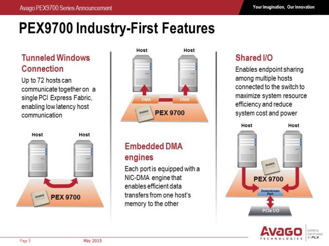
In the datacenter and within rack infrastructure, redundancy is a key feature to consider. As the PEX9700 switches allow host-to-host communication, it also allows control from multiple hosts, allowing one host to take over in the event of failure. The switches can also agglomerate and talk to each other, allowing for multiple execution routes especially with shared IO devices or in multiple socket systems for GPGPU use. Each switch will also have a level of hot-plugging and redundancy, allowing disabled devices to be removed, replaced and restarted. When it comes to IO, read requests mid-flow are fed back to the host as information on failed attempts, allowing instant reattempts when a replacement device is placed back into the system.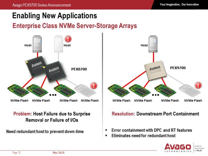
Avago is stating that the 9700 series will have seven products ranging from 5 to 24 ports (plus one for a management port) from 12 to 97 lanes. This also includes hot plug capability, tunneled connections, clock isolation and as mentioned before, downstream port isolation. These models are currently in full scale production, as per today’s announcement, using TSMC's 40nm process. In a briefing call today with Akber Kazmi, the Senior Product Line Manager for the PEX9700 series, he stated that validation of the designs took the best part of eight months, but that relevant tier one customers already have their hands on the silicon to develop their platforms.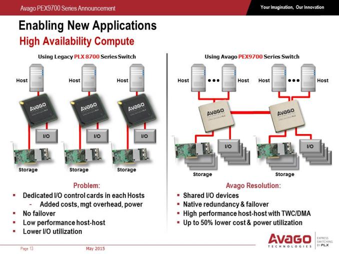
For a lot of home users, this doesn’t mean that much. We might see one of these switches in a future consumer motherboard focused on dual-socket GPGPU, but the heart of these features lies in the ability to have multiple nodes access data quickly within a specific framework without having to invest in expensive technologies such as Infiniband. Avago is stating a 150ns latency per hop, with bandwidth limited ultimately by the upstream data path – the PCIe switch ultimately moves the bandwidth around to where it is most needed depending on downstream demand. The PEX9700 switches also allow for direct daisy chaining or as a cascading architecture through a backplane, reducing costs of big switches and allowing for a peak bandwidth between two switches of a full PCIe 3.0 x16 interface, allowing scaling up to 128 Gbps (minus overhead).
Personally, the GPGPU situation interests me a lot. When we have a dual socket system with each socket feeding multiple GPUs, with one PEX9700 switch per CPU (in this case, PEX9797) but interconnected, it allows GPUs on one socket to talk to GPUs on the other without having to go all the way back up to the CPU and across the QPI bus, which saves both latency and bandwidth, and each of the PCIe switches can be controlled.
The PEX9700 series of switches bucks the status quo of requiring translation layers such as NICs or Infiniband for host-to-host-to-device communication and all inbetween, which is what Avago is hoping the product stack will accomplish. The main factors that Avago see the benefit include latency (fewer translation layers for communication), cost (scales up to 128 Gbps minus overhead), power (one PEX9700 chip has a 3W-25W power rating) and energy cost savings on top of that. On paper at least, the capabilities of the new range could potentially be disruptive. Hopefully we'll get to see one in the flesh at Computex from Avago's partners, and we'll update you when we do.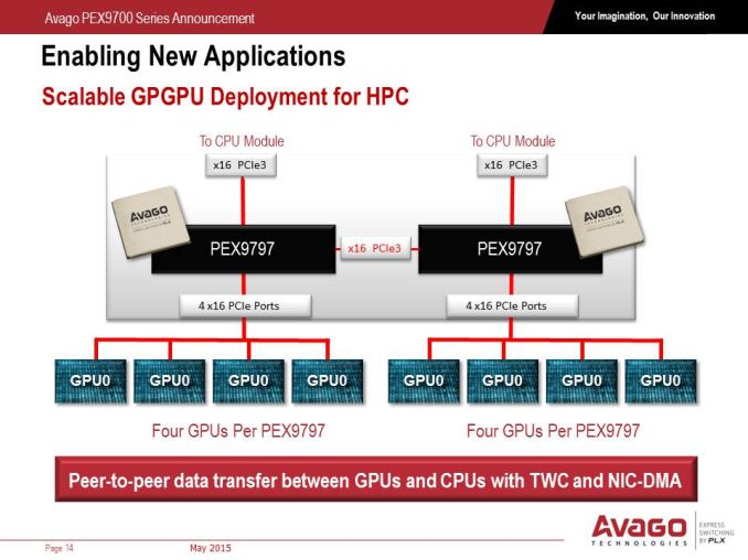
Source: Avago
Gallery: Avago Announce PLX PEX9700 Series PCIe Switches: Focusing on Data Center and Racks


More...
-
05-12-15, 05:01 PM #4989
Anandtech: NVIDIAs GRID Game Streaming Service Rolls Out 1080p60 Support
Word comes from NVIDIA this afternoon that they are rolling out a beta update to their GRID game streaming service. Starting today, the service is adding 1080p60 streaming to its existing 720p60 streaming option, with the option initially going out to members of the SHIELD HUB beta group.
Today’s announcement from NVIDIA comes as the company is ramping up for the launch of the SHIELD Android TV and its accompanying commercial GRID service. The new SHIELD console is scheduled to ship this month, meanwhile the commercialization of the GRID service is expected to take place in June, with the current free GRID service for existing SHIELD portable/tablet users listed as running through June 30th. Given NVIDIA’s ambitions to begin charging for the service, it was only a matter of time until the company began offering the service, especially as the SHIELD Android TV will be hooked up to much larger screens where the limits of 720p would be more easily noticed.
In any case, from a technical perspective NVIDIA has long had the tools necessary to support 1080p streaming – NVIDIA’s video cards already support 1080p60 streaming to SHIELD devices via GameStream – so the big news here is that NVIDIA has finally flipped the switch with their servers and clients. Though given the fact that 1080p is 2.25x as many pixels as 720p, I’m curious whether part of this process has involved NVIDIA adding some faster GRID K520 cards (GK104) to their server clusters, as the lower-end GRID K340 cards (GK107) don’t offer quite the throughput or VRAM one traditionally needs for 1080p at 60fps.
But the truly difficult part of this rollout is on the bandwidth side. With SHIELD 720p streaming already requiring 5-10Mbps of bandwidth and NVIDIA opting for quality over efficiency on the 1080p service, the client bandwidth requirements for the 1080p service are enormous. 1080p GRID will require a 30Mbps connection, with NVIDIA recommending users have a 50Mbps connection to keep from any other network devices compromising the game stream. To put this in perspective, no video streaming service hits 30Mbps, and in fact Blu-Ray itself tops out at 48Mbps for audio + video. NVIDIA in turn needs to run at a fairly high bitrate to make up for the fact that they have to all of this encoding in real-time with low latency (as opposed to highly optimized offline encoding), hence the significant bandwidth requirement. Meanwhile 50Mbps+ service in North America is still fairly rare – these requirements all but limit it to cable and fiber customers – so at least for now only a limited number of people will have the means to take advantage of the higher resolution.
As for the games that support 1080p streaming, most, but not all GRID games support it at this time. NVIDIA’s announcement says that 35 games support 1080p, with this being out of a library of more than 50 games. Meanwhile I’m curious just what kind of graphics settings NVIDIA is using for some of these games. With NVIDIA’s top GRID card being the equivalent of an underclocked GTX 680, older games shouldn’t be an issue, but more cutting edge games almost certainly require tradeoffs to maintain framerates near 60fps. So I don’t imagine NVIDIA is able to run every last game with all of their settings turned up to maximum.NVIDIA GRID System Requirements 720p60 1080p60 Minimum Bandwidth 10Mbps 30Mbps Recommended Bandwidth N/A 50Mbps Device Any SHIELD, Native Or Console Mode Any SHIELD, Console Mode Only (no 1080p60 to Tablet's screen)
Finally, NVIDIA’s press release also notes that the company has brought additional datacenters online, again presumably in anticipation of the commercial service launch. A Southwest US datacenter is now available, and a datacenter in Central Europe is said to be available later this month. This brings NVIDIA’s total datacenter count up to six: USA Northwest, USA Southwest, USA East Coast, Northern Europe, Central Europe, and Asia Pacific.
More...
-
05-13-15, 03:00 PM #4990
Anandtech: The Truth About SSD Data Retention
In the past week, quite a few media outlets have posted articles claiming that SSDs will lose data in a matter of days if left unpowered. While there is some (read: very, very little) truth to that, it has created a lot of chatter and confusion in forums and even I have received a few questions about the validity of the claims, so rather than responding to individual emails/tweets from people who want to know more, I thought I would explain the matter in depth to everyone at once.
First of all, the presentation everyone is talking about can be found here. Unlike some sites reported, it's not a presentation from Seagate -- it's an official JEDEC presentation from Alvin Cox, the Chairman of JC-64.8 subcommittee (i.e. SSD committee) at the time, meaning that it's supposed to act as an objective source of information for all SSD vendors. It is, however, correct that Mr. Cox works as a Senior Staff Engineer at Seagate, but that is irrelevant because the whole purpose of JEDEC is to bring manufacturers together to develop open standards. The committee members and chairmen are all working for some company and currently the JC-64.8 subcommittee is lead by Frank Chu from HGST.
Before we go into the actual data retention topic, let's outline the situation by focusing on the conditions that must be met when the manufacturer is determining the endurance rating for an SSD. First off, the drive must maintain its capacity, meaning that it cannot retire so many blocks that the user capacity would decrease. Secondly, the drive must meet the required UBER (number of data errors per number of bits read) spec as well as be within the functional failure requirement. Finally, the drive must retain data without power for a set amount of time to meet the JEDEC spec. Note that all these must be conditions must be met when the maximum number of data has been written i.e. if a drive is rated at 100TB, it must meet these specs after 100TB of writes.
The table above summarizes the requirements for both client and enterprise SSDs. As we can see, the data retention requirement for a client SSD is one-year at 30°C, which is above typical room temperature. The retention does depend on the temperature, so let's take a closer look of how the retention scales with temperature.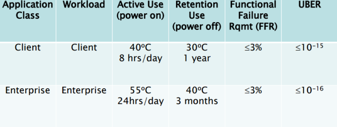
At 40°C active and 30°C power off temperature, a client SSD is set to retain data for 52 weeks i.e. one year. As the table shows, the data retention is proportional to active temperature and inversely proportional to power off temperature, meaning that a higher power off temperature will result in decreased retention. In a worst case scenario where the active temperature is only 25-30°C and power off is 55°C, the data retention can be as short as one week, which is what many sites have touted with their "data loss in matter of days" claims. Yes, it can technically happen, but not in typical client environment.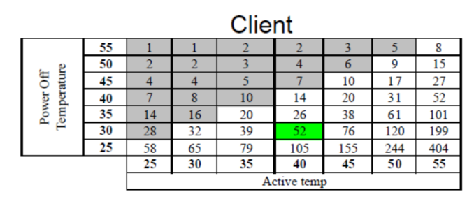
In reality power off temperature of 55°C is not realistic at all for a client user because the drive will most likely be stored somewhere in the house (closet, basement, garage etc.) in room temperature, which tends to be below 30°C. Active temperature, on the other hand, is usually at least 40°C because the drive and other components in the system generate heat that puts the temperature over room temperature.
As always, there is a technical explanation to the data retention scaling. The conductivity of a semiconductor scales with temperature, which is bad news for NAND because when it's unpowered the electrons are not supposed to move as that would change the charge of the cell. In other words, as the temperature increases, the electrons escape the floating gate faster that ultimately changes the voltage state of the cell and renders data unreadable (i.e. the drive no longer retains data).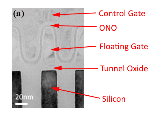
For active use the temperature has the opposite effect. Because higher temperature makes the silicon more conductive, the flow of current is higher during program/erase operation and causes less stress on the tunnel oxide, improving the endurance of the cell because endurance is practically limited by tunnel oxide's ability to hold the electrons inside the floating gate.
All in all, there is absolutely zero reason to worry about SSD data retention in typical client environment. Remember that the figures presented here are for a drive that has already passed its endurance rating, so for new drives the data retention is considerably higher, typically over ten years for MLC NAND based SSDs. If you buy a drive today and stash it away, the drive itself will become totally obsolete quicker than it will lose its data. Besides, given the cost of SSDs, it's not cost efficient to use them for cold storage anyway, so if you're looking to archive data I would recommend going with hard drives for cost reasons alone.
More...


 Quote
QuoteThread Information
Users Browsing this Thread
There are currently 21 users browsing this thread. (0 members and 21 guests)


Bookmarks