

Results 5,041 to 5,050 of 12091
Thread: Anandtech News
-
05-31-15, 05:30 PM #5041
Anandtech: NVIDIA Announces GameWorks VR Branding, Adds Multi-Res Shading
Alongside the GeForce GTX 980 Ti and G-Sync announcements going on today in conjunction with Computex, NVIDIA is also announcing an update for their suite of VR technologies.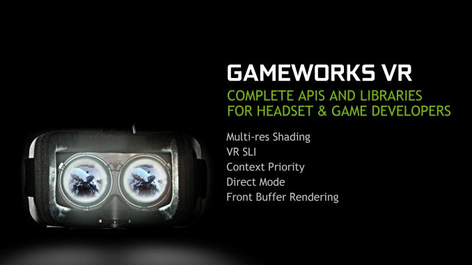
First off, initially introduced alongside the GeForce GTX 980 in September as VR Direct, today NVIDIA is announcing that they are bringing their VR technologies in under the GameWorks umbrella of developer tools. The collection of technologies will now be called GameWorks VR, adding to the already significant collection of GameWorks tools and libraries.
Multi-Res Shading
Meanwhile, alongside today’s rebranding, NVIDIA is also announcing a new feature for GameWorks VR: multi-resolution shading, or multi-res shading for short. With multi-res shading, NVIDIA is looking to leverage the Maxwell 2 architecture’s Multi-Projection Acceleration in order to increase rendering efficiency and ultimately the overall performance of their GPUs in VR situations.
The fundamental issue at play here is how rendering works in conjunction with the optics that go into a VR headset. VR headsets uses lenses to help users focus on a screen mere inches from their eyes, and to help compensate for the wide field of vision of the human eye. However in doing this, these lenses also introduce distortion, which in turn must be compensated for at the rendering phase in order to similarly distort the image such that it appears correct to the user after going through the lenses.
From a rendering perspective none of this is problematic, as distorting a rendered image is actually a pretty straightforward pixel shader operation. However one of the products of this distortion is that the distorted image has less information in it than the original image, due to the combination of the presence of optics in a headset and the fact that the human eye sees more detail at the center than at its edges. The end result is that GPUs are essentially rendering more detail than they need to at the edges of a frame, which in turn introduces some room for psychovisual rendering optimizations.
This brings us to multi-res shading and the theory behind this feature. The crux of the theory behind multi-resolution rendering is that if a GPU could render parts of a single frame at differing levels of detail – a full-detailed center and a lower detailed peripheral – then that GPU could reduce the overall amount of work required to render a frame, boosting performance and/or lowering the GPU requirements for VR. Rendering a frame in such a fashion would result in a loss of image quality – a subdivided image rendered at different detail levels would not be identical to a traditionally rendered full-detail image – but since image quality is compromised by the distortion itself and the compromised portions of the image are being directed at the less-sensitive outer edges of the eye, the end result is that one can bring down the detail level of the outer edge of an image without significantly compromising the projected image or the user experience. Think of it as lossy compression for VR.
For multi-res shading NVIDIA does just this, leveraging their multi-projection acceleration technology to efficiently implement it. In this process NVIDIA subdivides the image into multiple viewports, scaling the outer viewports to lower resolutions while rendering the inner-most viewport at full resolution, resulting in an image that overall is composed of fewer pixels and hence faster to render. MPA in turn allows NVIDIA to build the scene geometry a single time and project it to the multiple viewports simultaneously, eliminating much of the overhead that would be incurred in rendering the same scene multiple times to multiple viewports.
The end result of multi-res shading is that NVIDIA is claiming that they can offer a 1.3x to 2x increase in pixel shader performance without noticeably compromising the image quality. Like many of the other technologies in the GameWorks VR toolkit this is an implementation of a suggested VR practice, however in NVIDIA’s case the company believes they have a significant technological advantage in implementing it thanks to multi-projection acceleration. With MPA to bring down the cost of rendering to multiple viewports, NVIDIA’s hardware can better take advantage of the performance advantages of this rendering approach, essentially making it an even more efficient method of VR rendering. Of course it’s ultimately up to developers whether they want to implement this or not, so whether this technology sees significant use is up to developers and whether they find the tradeoffs worth the performance gains and necessary development effort.

More...
-
05-31-15, 11:30 PM #5042
Anandtech: ARM Announcements: New IoT Subsystem for TSMC 55ULP and ARM Cardio Radio I
Today at Computex ARM is announcing a new 'IoT Subsystem' for developers: ARM Cortex-M with ARM Cordio radio IP (see below) with full integration with mBed OS. The principle behind this licencable IP block is to allow developers an end-point to integrated sensors and other peripherals on the route to design a complete SoC. The ARM Artisan physical IP, a flash technology for low power operation, is produced in conjunction with TSMC's 55nm Ultra-Low-Power process for embedded flash memory. 55nm sounds like a large process, but for a lot of IoT type devices it provides a mix of power, price and performance, particularly when an ultra-low-power process node is placed in the mix.
ARM's goal here is to provide a solution to its customers. ARM's business model revolves around licencing either their instruction set or the blueprints for partners to design their own SoCs. However, if we considered a saturated top tier market for processor IP, the way to grow with mid and low range partners is to provide more complete solutions. This is ARM's goal here with the IoT Subsystem, especially when IoT and 'billions of units' are spoken often in the same sentence more often. ARM also likes to note that by investing in a more complete subsystem, developers can reduce elements of risk with SoC design.
Because companies like ARM are more often the start point when it comes to developing devices around the internet of things, it can be difficult for them to drive the end products. Personally, I feel that while IoT is spoken about often at events, we don't always see the end product in ours hands in the volumes that are quoted. Part of that is the ecosystem, which needs to evolve. Offering more complete start points is one element of that process.
With reference to ARM Cordio, this is a new IP portfolio from ARM as a direct result of acquiring two companies - Wicentric and Sunrise Micro Devices, as formally announced a couple of weeks ago. This includes Bluetooth smart software solutions for low power wireless products as well as radio IP including pre-qualified, self-contained radio block with related firmware. The Cordio IP with TSMC 55ULP is rated to get over 2x more life over 1.2 volt and up when Lithium batteries are used. Dr Dinesh Patel, the VP of Technical Operations at ARM, showed off a radio beacon device built on the basis of Cordio at ARM's press event today.
Source: ARM

More...
-
06-01-15, 12:44 AM #5043
Anandtech: SanDisk Announces 2TB USB 3.1 External SSD
SanDisk is announcing the availability of a host of external flash drives at Computex 2015. Two of them are being marketed as external portable SSDs with a Type-C interface, while the other two are standard flash drives.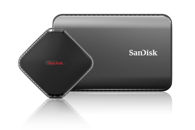
The SanDisk Extreme 900 Portable SSD is the obvious star of the lineup. It comes in three capacities, 480 GB ($400), 960 GB ($600) and 1.92 TB ($1000). The SSD is housed inside a compact aluminum casing. All of them carry three year warranties. The family comes with a maximum performance rating of 850 MBps and carries a USB 3.1 interface. Both Type-A and Type-C cables are supplied with the unit.
Aspects of interest include whether the internal flash is organized in a RAID-0 fashion with SATA interfaces, or whether it is a PCIe based unit behind a USB 3.1 controller. Kristian is at Computex and will likely be having some hands-on time with the device to gather the answers
The SanDisk Extreme 500 Portable SSD is available in 120 GB ($100), 240 GB ($150) and 480 GB ($240) capacities and claims maximum performance of 415 MBps via a USB 3.0 interface. Both Portable SSDs are designed for rugged environments and feature SanDisk SecureAccess software with 128-bit AES encryption.
The Ultra Fit 128 GB and Ultra 256 GB are standard USB 3.0 thumb drives. The Ultra Fit is more like the Mushkin Atom in size, but has double the capacity. The unit is priced at $120. The maximum performance is of the order of 130 MBps. The Ultra Fit 256 GB is rated for 100 MBps and is priced at $200.
Both the Ultra thumb drives carry a five year warranty and include encryption with the SecureAccess software. In addition, these drives come with a year's subscription to RescuePRO software for data recovery.
More...
-
06-01-15, 01:42 AM #5044
Anandtech: ASUS Shows Off The ZenWatch 2 At Computex
Today ASUS updated their Android Wear smartwatch offering. It wasn't long ago that we saw the original ASUS ZenWatch at IFA, but it's now being superseded by the ZenWatch 2. Unfortunately, details are fairly scarce about ASUS's new watch. It's powered by an unnamed SoC from Qualcomm, and sports a 2.5D AMOLED display of unknown size. More details about the ZenWatch 2 should come out over the course of Computex.
One area where the ZenWatch 2 is clearly improved over its predecessor is the water and dust resistance. The original ZenWatch had an IP55 rating, and this has been improved to an IP67 rating for greater water submersion protection.
The ZenWatch 2 comes in two sizes, and both models come in silver, gunmetal, and rose-gold finishes. Straps are available in rubber, leather, and metal. One interesting feature on the larger model is that it can be used as a tiny battery power pack to charge your phone, but with the limited battery capacity of smartwatches this seems like something to only be used as a last resort.
More...
-
06-01-15, 01:42 AM #5045
Anandtech: ASUS Announces Two New 8 Inch ZenPad Tablets
ASUS is no stranger to the Android tablet market. They've been around since the earliest days of Android tablets with their ASUS Transformer TF101 which launched with Android Honeycomb. Since that time they've released a number of iterations of the ASUS Transformer Android tablet, and have also expanded to other parts of the market with tablets like the ASUS MeMO Pad. In addition to their independent endeavors, they worked with Google to design and manufacture both generations of the Nexus 7, which was beloved by Android enthusiasts.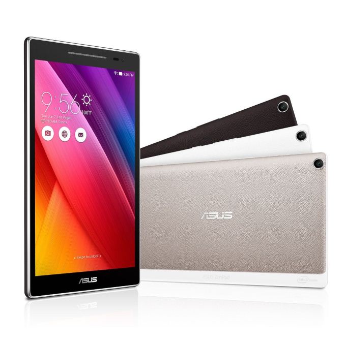
While ASUS has been making Android tablets for a while, it has also been quite some time since we've seen a high end tablet come from the company. A focus on expansion into the world of Windows tablets has left the spot for a high end ASUS tablet unfilled. However, with a renewed focus on expanding their role as an Android manufacturer, and global ambitions with devices like the ZenFone 2, it was only a matter of time before ASUS brought new Android tablets to market. It also seemed inevitable that those devices would now fall under ASUS's Zen branding, and indeed, they do. ASUS's new Android tablets are the first in a line of tablets under the ZenPad brand.
To put things in perspective and make it easier to compare these two new tablets, I've organized their general specifications in the chart below. There are a few things missing at the moment as they haven't yet been provided by ASUS, but I will update the chart and this article as soon as they are known.
With this launch it appears that ASUS is putting devices into play at both the high end and the low end of the tablet market. The ZenPad Z380 is certainly the thicker of the two devices, and it's slightly shorter but with a much more narrow profile. You can see the ZenPad Z380 pictured in the cover image above, and the ZenPad S Z580CA is down below. While the Z380 opts for swappable leather textured backs, the Z580CA has a non-removable metallic back, although it's unknown if it's actually made of metal. I'll start by talking about the Z380 before moving onto the Z580CA.ASUS ZenPad 8 (Z380) ASUS ZenPad S 8 (Z580CA)SoC Intel Atom x3-C3230RK
4x Silvermont @ 1.2GHzIntel Atom Moorefield Z3580
4x Silvermont @ 2.33GHzGPU ARM Mali 450 MP4 PowerVR G6430 @ 533MHz RAM 1 or 2GB LPDDR3 4GB LPDDR3 NAND 8/16GB + microSDXC 16/32/64GB + microSDXC Display 8.0" 1280x800 IPS LCD 8.0" 2048x1536 IPS LCD Dimensions 209 x 123 x 8.5mm 203.2 x 134.5 x 6.68mm Mass ? 299g Camera 2MP Front-facing
5MP Rear-facing5MP Front-facing
8MP Rear-facingBattery 15.2Wh OS Android 5.0 Lollipop with ASUS Zen UI Other Connectivity 802.11b/g/n + BT 4.0, GNSS Cellular LTE SKU with phone functionality WiFi Only USB Connector Micro USB USB Type-C
The first thing I noticed about the ZenPad Z380 was that it uses the Intel Atom x3-C3230RK SoC. This is a very interesting chip, because the RK on the end of the name signifies that it's a chip designed by Rockchip rather than Intel. Through their partnership, Intel licenses their architecture to Rockchip to use in the SoCs they design, and those SoCs are then fabricated on TSMC's 28nm process. It's a surprising collaboration of three companies.
Atom x3-C3230RK has four of Intel's Silvermont cores and they have a peak frequency of 1.2GHz. This puts it pretty far behind Intel's higher clocked Moorefield parts that are built on their 22nm manufacturing process when it comes to bursty workloads. However, the size of the gap between it and Moorefield will be in a sustained load when both SoCs throttle down remains to be seen. It also sports ARM's Mali 450 GPU with four cores, although the clock speed on those GPU cores is unknown.
Moving on from the SoC, we see that the ZenPad Z380 comes with either 8GB or 16GB of internal memory, and 1GB or 2GB of RAM. According to ASUS, these specs can vary based on region, so be sure to take a look at the spec sheet if you plan on buying the Z380. It also has an 8" 1280x800 IPS LCD which is fairly standard for a low end tablet, and a pair of 2MP and 5MP cameras on the front and back respectively.
After the ZenPad Z380 comes the high end ZenPad S Z580CA, which is also a tablet with an 8" display. However, the fact that both of these tablets have the same display size as measured from corner to corner does not mean they have the same form. This is because the ZenPad S uses an 8" 2048x1536 IPS panel which has a 4:3 aspect ratio. ASUS is following HTC and Samsung in moving to 4:3 after many years of 16:10 Android tablets. I'm surprised that it took this long for vendors to realize that 16:10 is ill suited to many of the tasks users perform on tablets and makes a device more difficult to manage in varying orientations.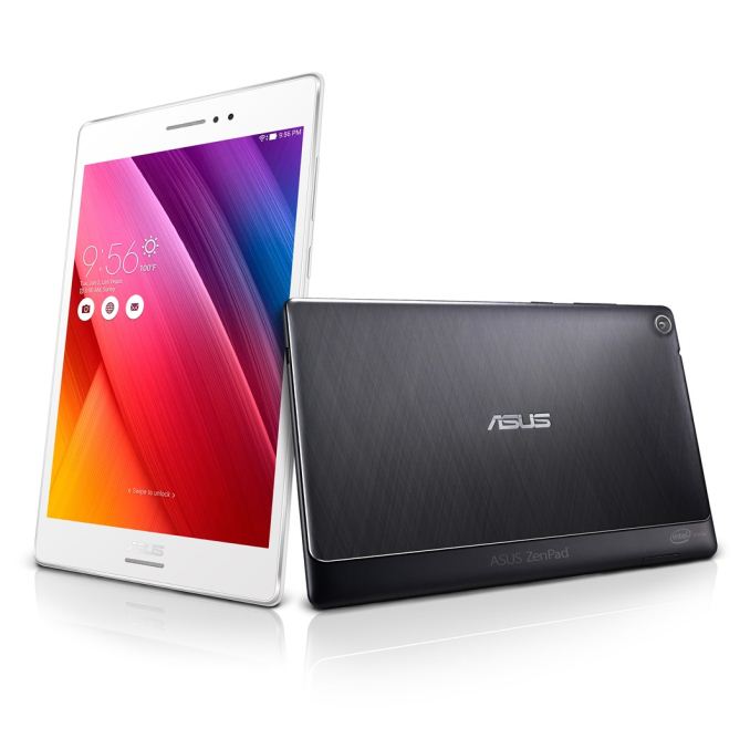
The rest of the internal specifications of the ZenPad S are very similar to those of ASUS's ZenFone 2. It uses Intel's Atom Z3580 SoC which is a 22nm part with four Silvermont cores that run at up to 2.33GHz, along with a PowerVR G6430 GPU at 533MHz. Other specs include up to 64GB of NAND, 4GB of LPDDR3 memory, a 5MP front camera, and an 8MP rear camera.
Both of these new ZenPads share the same battery capacity, which is somewhat concerning when one considers that the display on the ZenPad S will most likely consume more power than the ZenPad Z380. They also share the same WiFi, and in both cases it's a very disappointing 2.4GHz 802.11n part. Although lackluster WiFi is not new to ASUS products on the laptop side with devices like the Zenbook UX305, the ZenFone 2's 802.11ac support had me hoping that this wouldn't extend to their mobile devices as well. While pricing for both these new tablets hasn't been revealed, the Z580CA is clearly aimed at the high end, and when your $199 ZenFone 2 has 802.11ac your high end tablet should too.
There is one final thing that distinguishes the ZenPad S Z580CA from the Z380, as well as from almost any other tablet. It's the use of the new USB Type-C standard for charging and data connections, with no MicroUSB port available. This is probably going to be painful for some consumers as charging cables get lost or broken and can't be replaced with easily available MicroUSB cords, but it's a transition that needs to happen and I applaud ASUS for beginning it sooner rather than later. Using the Type-C port for connecting peripherals or doing display output will definitely be something to investigate if we do a review of the ZenPad Z580CA in the future. When Android M rolls around it will also be interesting to see if you can use the ZenPad Z580CA to charge another device.
ASUS has also announced a range of accessories for these new tablets. The Z380 has protective cases available, and an audio cover that ASUS says enables 5.1 surround sound, powered by the ZenPad's build in DTS codec. There's also a power case to extend the tablet's battery capacity, and a 1024 pressure level stylus which works with both of the new ZenPad tablets.
Overall I think ASUS has two very interesting devices on their hands. For me the ZenPad S is the most interesting of the two because of its hardware and USB Type-C connector, but the ZenPad Z380 could prove to be a formidable competitor to other inexpensive Android tablets depending on its price. Speaking of price, that's another aspect about these tablets that is currently unknown. Much of the success of these new tablets will be based on whether they provide a good value relative to their price. ASUS has a lot of competition, but if these tablets are priced right they could have a couple of winning tablets on their hands.
More...
-
06-01-15, 03:09 AM #5046
Anandtech: MediaTek announces Helio P10 Mainstream SoC
MediaTek started promoting its new Helio branding for SoCs back at MWC this year, and we had the please to cover the the new Helio X20 announcement just a few weeks ago. While the X-series is supposed to target the higher end (dubbed "eXtreme Performance"), the P-line is aimed at the budget mid-range ("Premium Performance" as MediaTek calls it). Today's announcement of the Helio P10 marks the first SoC in the P-series to adopt the new branding.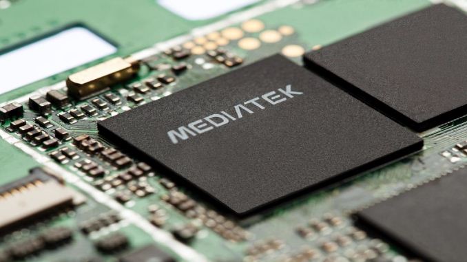
The P10 is the direct successor to last year's MT6752, which saw some quite widespread in adoption by Chinese vendors such as Meizu (M1 note), Gionee (Elife S7) or JiaYu (S3) and others. The P10 improves on its predecessor, the the MT6752, by taking a lot of improvements which were introduced with the X10 and X20.
On the processor side, the CPU configuration remains a dual-cluster with four A53 cores per cluster. The MT6752 clocked both clusters at the same clock, running from 1.7 up to 2.0GHz as its maximum frequency depending on the chip bin. The P10 keeps this 2.0GHz maximum clock for its performance cluster, but has a slower cluster at lower speeds which we weren't yet able to confirm with MediaTek.
Memory bandwidth was supposedly also increased, and I suspect, but again in need of confirmation, that we're talking about finally switching over to a dual-channel memory controller, as the MT6752 was still sporting a single 32bit controller. The P10 is aimed at 1080p devices so it looks that MediaTek is keeping the graphics performances conservative and power efficient.MediaTek 2015 Main Lineup SoC MediaTek
Helio X20
(MT6797)MediaTek
Helio X10
(MT6795)MediaTekHelio P10MediaTekMT6752CPU 4x Cortex A53 @1.4GHz
4x Cortex A53 @2.0GHz
2x Cortex A72
@2.3-2.5GHz4x Cortex A53 @2.2GHz
4x Cortex A53 @2.2GHz4x Cortex A53
@lesser freq
4x Cortex A53 @2.0GHz4x Cortex A53
@1.7-2.0GHz
4x Cortex A53
@1.7-2.0GHzMemory
Controller2x 32-bit @ 933MHz
LPDDR3
14.9GB/s b/w2x 32-bit @ 933MHz
LPDDR3
14.9GB/s b/w2x 32-bit @ 800+MHz
LPDDR3
12.8+GB/s b/w
(To be confirmed)1x 32-bit @ 800MHz
LPDDR3
6.4GB/s b/wGPU Mali T8??MP4
@700MHzPowerVR G6200
@700MHzMali T860MP2@700MHzMali T760MP2
@728MHzEncode/
Decode2160p30 10-bit
H.264/HEVC/VP9
decode
2160p30
HEVC w/HDR
encode2160p30 10-bit
H.264/HEVC/VP9
decode
2160p30
HEVC
encode1080p30H.264 & HEVCdecode
1080p30H.264encode1080p30H.264 & HEVCdecode
1080p30H.264encodeCamera/ISP Dual ISP
32MP @ 24fps21MP single or16MP + 8MP dual21MP single or
16MP + 8MP dual16MP Integrated
ModemLTE Cat. 6
300Mbps DL
50Mbps UL
2x20MHz C.A.
(DL)LTE Cat. 4
150Mbps DL 50Mbps ULLTE Cat. 6300Mbps DL
50Mbps UL
2x20MHz C.A.(DL)LTE Cat. 4150Mbps DL
50Mbps UL
MediaTek also upgrades the GPU from a Mali T760 to a T860, but keeps the shader core count steady at 2. We again see some interesting power claims concerning the T8XX series as MediaTek claims the new GPU uses only 70% of the power of the previous T760 iteration while improving performance by 20%, but we might be not talking solely architectural improvements as the P10 comes on a brand-new silicon manufacturing node.
The P10 is the first SoC to be announced on TSMC's 28HPC+ process. TSMC published the 28HPC process last autumn as a successor to 28HPM - with the advantages of a slight die shrink and improved power characteristics. 28HPC+ is yet another iteration that was publicly talked about last April, and promises a 15% gain in performance or a quite large 30 to 50% reduction in leakage at the same speed when compared to 28HPC.
We'll continue to see the 28nm process continue to live on for a long time in the mid-range and cost-sensitive segments as it marks the sweet-spot in the transistors/$ scaling, and 28HPC(+) is one of the first enablers of this life-time extension.
The Helio P10 also takes over the modem sub-system that we've seen announced in the X20 - with LTE rel.11 Category 6 capability and 2x20MHz carrier aggregation on the download stream. This also includes crucial CDMA2000 support that MediaTek needs to be able to penetrate the North American and other limited markets.
The mainstream lineup is the Taiwanese company's bread & butter and is the source of where MediaTek has seen most of its notorious successes. The P10, being part of this segment, will very likely see similar widespread adoption in low-cost devices as the Chinese smartphone boom continues to grow.
The Helio P10 is supposed to be sampling in early Q3 2015 and with phone mass-production happening towards the end of the year in the fourth quarter.
More...
-
06-01-15, 04:13 AM #5047
Anandtech: Microsoft Announces That Windows 10 Will Launch On July 29
Today Microsoft formally announced the release date for Windows 10, the latest version of their Windows operating system. Up until this point, all Microsoft had said was that they were aiming for a summer release. Today's post on the official Windows blog states the release date for Windows 10 has now been set for July 29, less than two months from now.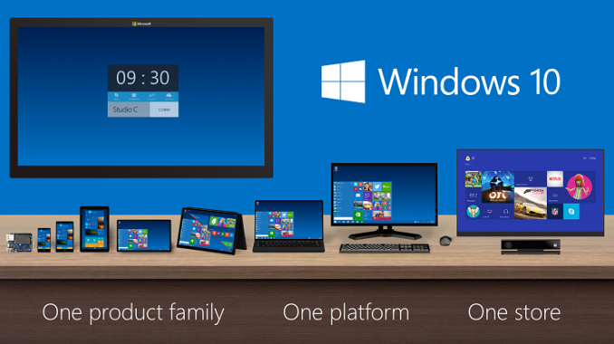
According to the blog post, Microsoft expects Windows 10 to usher in a new era for 1.5 billion Windows users that currently reside in over 190 different countries. Windows 10 is Microsoft's chance to win back users who didn't embrace the changes made in Windows 8, and they have a lot riding on its success. Offering it as a free upgrading to existing Windows users will certainly help in gaining adoption.
Even with the free nature of the upgrade, the promise of a July release date for such a monumental update is quite a bold move on Microsoft's part. The less than optimal state of the current Windows 10 testing builds means that Microsoft has a great deal of work ahead of them as they squash bugs and improve the stability of Windows 10 in the two months between now and release. As a user who is keen on upgrading from Windows 7 to Windows 10, I really hope they succeed.

Finally, Microsoft has revealed a few more details about how Windows 10 distribution will work. Starting today, users can "reserve" Windows 10 on Windows 7/8.1 machines. Reserving Windows will in turn flag a machine for pre-loading, with Microsoft distributing most of Windows 10 ahead of time as to get it in to customers' hands more quickly to better balance the expected load on their server backend. According to Microsoft's FAQ, reserving/pre-loading Windows 10 only downloads it, and users will still manually confirm the installation, or for that matter users can cancel the reservation entirely. Pre-loading has not started yet, and while Microsoft doesn't say when it will start, I expect it won't be until very near July 29th.
Along with detailing the reservation process, Microsoft has also confirmed the upgrade paths for various versions of Windows. As expected, all Pro/Ultimate versions of Windows 7 and 8.1 will get upgraded to Windows 10 Pro, while all other versions of desktop/tablet Windows will get upgraded to Windows 10 Home. And of course, Windows Phone 8.1 devices will upgrade to Windows 10 Mobile.
Windows 10 Upgrade Paths Win10 Win7 Win8.1 Windows 10 Home Win7 Starter Windows 8.1 (Core) Win7 Home Basic Windows 8.1 (Country-Specific) Win7 Home Premium Windows 8.1 w/Bing Windows 10 Pro Windows 7 Professional Windows 8.1 Pro Windows 7 Ultimate Windows 8.1 Pro for Students Windows 10 Mobile N/A Windows Phone 8.1
More...
-
06-01-15, 10:00 AM #5048
Anandtech: Corsair unleashes the Bulldog DIY 4K Gaming PC
Corsair certainly is a company that is not afraid of diversification and has proved that multiple times in the past. They started as a memory products manufacturer, diversified into the power, case and cooling market segments and today they even have their own gaming division.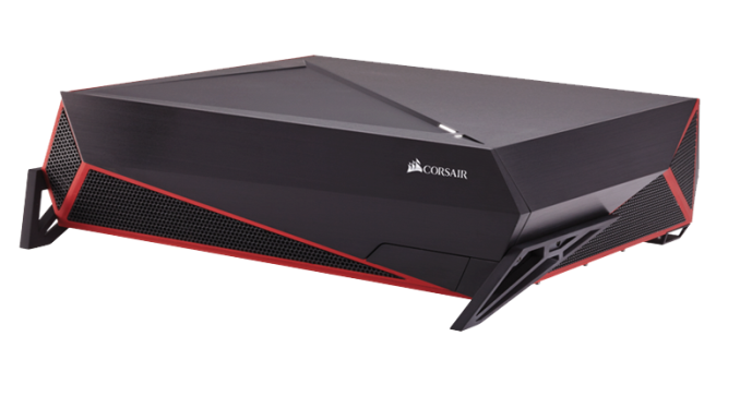
With a company as active as Corsair is, their latest move was no surprise to us. Corsair combined their knowledge of chassis design and thermal performance, used their industry contacts and brought about the creation of the Bulldog, a DIY 4K Gaming PC designed to fit into living rooms.
The Bulldog is the combination of a desktop PC case styled to appear as a gaming console with a 600W SFX power supply, a liquid cooler for the CPU and an ITX motherboard. Corsair's aim was to reduce a very high performance gaming PC to fit within the dimensions of a gaming console. In order to do that, they managed to fit dual liquid cooling systems (one for the CPU and, optionally, one for the GPU) and a high output SFX PSU into the desktop chassis. In terms of size, the Bulldog is relatively small but not too small, as it had to be tall enough for a high-end graphics card to fit.
The base configuration of the Bulldog includes the case, the ITX motherboard, the H5SF CPU liquid cooler and the 600W SFX power supply. It starts with a MSRP of $399, which seems a little steep at first but it is not really overpriced considering the specs of the motherboard. We are not aware of very specific details regarding the motherboard that is installed in the Bulldog, but it will support DDR4 RAM, USB 3.1, 7.1 audio, Gigabit Ethernet and WiFi. (It's worth noting that at this point, the only mini-ITX motherboard that can support DDR4 is the ASRock X99E-ITX, but in the pictures provided by Corsair the board used seems to be a DDR3 based ASUS. It doesn't take much to pinpoint that the Bulldog is mostly likely aimed for a future DDR4 capable platform, or currently just for the ASRock motherboard if Corsair wishes to pursue the DDR4 route exclusively.) Corsair has also collaborated with NVIDIA and MSI to create drop-in ready liquid cooled variations of the Geforce GTX Titan X, GTX 980, GTX 980 Ti and GTX 970. Combinations of the Corsair H55 liquid AIO cooler and the HG10 graphics card cooling bracket may also be used.
Corsair's timing with that release seems perfect, as the first few graphics cards that can borderline handle 4K gaming are just hitting the market. A few months ago and 4K gaming without at least two high-end GPUs installed was impossible. However, you cannot install two graphic cards in a system with an ITX motherboard, which made the creation of very small 4K gaming PCs very difficult. Aesthetically, we feel that many will question the overly aggressive appearance of the Bulldog for a machine that is meant to be into living rooms. It definitely stands out a lot and that is not what people with modernized/minimalistic interior designs want. However, if Corsair's endeavor proves to be successful, it would be rather easy for them to base other designs on this, offering new products to cover a variety of tastes.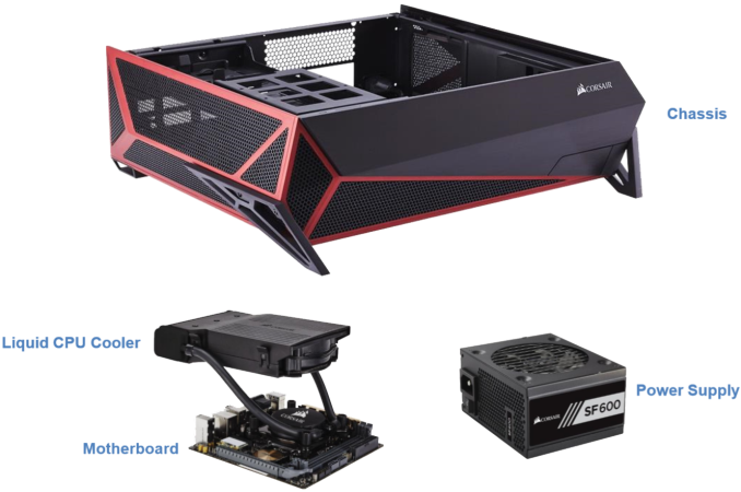
Alongside with the Bulldog, Corsair is also releasing the Lapdog, a gaming control center for use in the living room. Long story short, the Lapdog is a wired keyboard/mouse dock designed to sit on someone's lap. Aside from the presence of a USB hub and the memory foam cushion for user comfort, we do not have many details about the Lapdog at this point of time. Corsair will be offering it as a standalone station for $89 or with a keyboard for $199. The included keyboard obviously is the Corsair Gaming K65 RGB but we are unaware regarding the Lapdog's compatibility with other keyboards.

More...
-
06-01-15, 11:31 AM #5049
Anandtech: The Kaveri Refresh 'Godavari' Review: Testing AMD's A10-7870K
Astute readers will recognize that we recently posted two reviews covering more of the stack of AMD processors with the codename 'Kaveri' which covered the A6-7400K, A8-7650K and the A10-7700K in our recent coverage. Today we review the newest element that sits on top of all others, the A10-7870K Kaveri Refresh APU.
More...
-
06-01-15, 05:30 PM #5050
Anandtech: Intel to Acquire FPGA-Specialist Altera for $16.7 Billion
Today Intel has announced that they are buying Altera in an all-cash deal of $16.7 billion. The deal, having been rumored for a while now, will see Intel pick up Altera for their Field Programmable Grid Array (FPGA) experience, with Intel intending to both continue FPGA development integrating FPGAs into some of their future products.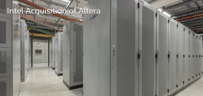
In the FPGA space Altera is one of the two major competitors, and alongside rival Xilinx compose the two companies comprise the bulk of the market. Prior to this sale Altera already had a close relationship with Intel, with Altera using Intel’s 14nm process for their latest generation of Stratix FPGAs.
As one of only a few external companies known to be using Intel’s 14nm process, Altera’s FPGA’s have been a natural complement to Intel’s ASIC business. On a business side there’s minimal overlap, but more importantly on the technical side FPGAs are good candidates for early production on a lower-yielding node. Since FPGAs are just large arrays of programmable logic and RAM, they can easily compensate for defects, allowing for a greater number of chips to be shipped for revenue early-on than a more complex ASIC.
Given Intel and Altera’s already close working relationship, today’s deal was not unexpected. Purchasing Altera allows Intel to bring their FPGA production entirely in-house, not just producing FPGAs but better aligning them to Intel’s development plans as part of their integrated device manufacturing model. However more significantly, this gives Intel access to top-tier FPGA technology, which they can use to augment other products. Intel is already talking about the possibilities they see for Altera’s FPGA technology in the IoT and datacenter markets, but also the company has confirmed that they will be integrating FPGA technology into some of their future Xeon products, to allow customers to essentially build-out semi-custom processors via the FPGA component. Intel already does on-package FPGAs for certain customers, so this would represent the logical extension of that process by bringing the FPGA fully on-die.
For Intel this also represents a chance to further branch out in the markets they cover. The PC and server market has continued to treat the company well, even as PC sales have slowed, but having so far struggled to capture a major piece of the mobile space from ARM and its partners, Intel has been looking at other avenues of growth. In this case FPGAs represent a high-margin business on their own, one that’s increasing in revenue as ASIC development costs continue to rise, and a good match for Intel given their traditional manufacturing advantage.
More...


 Quote
QuoteThread Information
Users Browsing this Thread
There are currently 11 users browsing this thread. (0 members and 11 guests)


Bookmarks