

Results 5,231 to 5,240 of 12096
Thread: Anandtech News
-
08-07-15, 02:30 PM #5231
Anandtech: Verizon Eliminates Contracts and Device Subsidies
North America has always had a fairly unique pricing structure for buying mobile devices. In many places, the concept of purchasing a device for a heavy subsidy and committing to stay with a given carrier for two or three years is unheard of, but in the United States and Canada it has always been the norm. However, that dynamic has been changing as it has become more difficult for operators to subsidize expensive smartphones for the wide market of consumers. Both T-Mobile and AT&T have moved away from the original model of contracts and subsidies in favor of installment plans or simply selling devices at full price, and today Verizon announced that they will follow in their footsteps.
With Verizon's new plans, there are no more contracts and no more device subsidies. Instead, consumers pay for their phones, pay for a bucket of data, and then pay a fee for each device that they add onto the account. The base monthly data fees are 1GB for $30, 3GB for $45, 6GB for $60, and 12GB for $80. On top of the data bucket fee, users will pay $20 to add a smartphone to the account, $10 for a tablet/data stick, and $5 for a smartwatch with cellular capabilities. Additional data over the limit will cost $15 per gigabyte,
As for existing consumers, Verizon will apparently offer avenues for them to get another subsidized device when they transition to these new plans, and they can also hold onto their older plans if they desire. Verizon customers interested in the new plans can switch over when they go live on August 13.
More...
-
08-10-15, 02:30 AM #5232
Anandtech: Aleutia Updates R50 and T1 Fanless Industrial PCs with Partial Copper Chas
Aleutia's fanless industrial PCs have seen deployment in a large number of developing countries as well as other extreme environments, thanks to their rugged nature and low power requirements. We reviewed the Aleutia Relia back in 2012, but, since then, a number of new models have been launched - the Aleutia R50 based on the NUC platform, the Aleutia T1 based on the Intel Atom lineup and the M200 fanless 2U servers with Intel Xeon CPUs.
In an attempt to improve the thermal performance of their fanless computing systems, Aleutia has decided to go in for a novel chassis design along with their latest updates to the R50 and T1 families. The R50 is still based on the NUC platform, but the T1 moves to a nano-ITX design.
Traditional passively cooled systems involve a copper heatsink on the CPU transferring the heat to a larger chassis (made of steel or aluminum) through copper heat pipes. Copper heat sinks are quite costly (relative to the cost of the system as a whole) as one goes for bigger / heavier ones. Aleutia has re-imagined the chassis by developing a copper heat sink that has the same profile as the chassis itself (made clear in the photograph below). The Aleutia R50 Broadwell NUC
The holes in the heat sink help it get connected to the rest of the chassis. On the whole, this lends to theoretically better thermal performance and also lends a striking look to both the R50 and T1 PCs. In addition, the presence of more copper for heat dissipation purposes has allowed Aleutia to reduce the volume of the R50 by 24% compared to the Haswell version. We are excited to check out the thermal performance of these PCs once they start shipping later this month.
In terms of the internal platform itself, the R50 now comes with the Broadwell i3 and i5 (15 W TDP) NUC configurations, while the new T1s will be based on the Bay Trail Celeron J1800 (10 W TDP). The new R50 will come in at £599 for the i3 / 8GB / 128GB configuration - reasonable for industrial PCs, but not the average retail consumer. The T1 will come in around £100 - £200. We should have more information and hands-on time at the Intel Developer Forum later this month. The Aleutia T1 Bay Trail Nettop
More...
-
08-10-15, 05:01 AM #5233
Anandtech: Intel Quietly Launches Mobile Xeons: Skylake Based E3-1500M v5
In a rather understated blog post, Intel made an interesting move at the end of last week by announcing that for the first time the Xeon platform is heading for mobile workstation platforms.
When I first heard this, I thought ‘wait, is it not already?’, given that I have seen laptops with Xeon processors in the past. The fact of the matter is that those previous platforms relied on desktop processors (either socketed or soldered) from the high end line and were only ever found in custom designs such as those from Clevo or Eurocom which promoted a more modular concept. As a result, these systems were typically heavy, demanding, and featuring more cores/cache/TDP than was expected for a laptop. We also saw consumer processors for notebooks with vPro, but these were typically not ECC memory verified. Intel’s announcement today changes this.
With specific mobile processors going Xeon, Intel can forge (with OEMs) a line of workstations that are more akin to the ultrabooks and notebooks we already see in the market but with certified professional level features. Intel is stating that by default all E3-1500M v5 processors will have vPro (which was to be expected) as well as Thunderbolt 3 using Type-C and access to ECC memory. So it does not become hard to imagine a professional version of the Dell XPS 13 or a MacBook / MacBook Professional type device that looks like a Core-M or a 15W clamshell with Thunderbolt 3, and/or ECC memory, while also having hardware-assisted security and ISV workstation level certification. It is our understanding we might expect announcements on specific products from manufacturers in the coming weeks.
This announcement does not give details about what types of processors (if they might be dual core, quad core, or have eDRAM) will be coming to the market, only that the mobile workstation market (according to IDC’s most recent report) has showed its sixth straight quarter of year-over-year growth which is a big pointer into the decision to release Xeon on mobile. We will be getting more details as time progresses – with Intel’s Developer Forum conference a week away, we may hear something then.
Source: Intel
More...
-
08-10-15, 05:31 AM #5234
Anandtech: Skylake CPU Package: Mini-Analysis
As a short side piece from our in depth review on Intel's 6th Generation Core processors, codename Skylake, the well-known overclocker Splave has posted some very interesting images on the processor itself. We confirmed we are free to use the pictures below from him.
First up is an image of the Skylake i7 silicon die on package. With our trusty interpolation measuring skills, the die area for the GT2 enabled quad core system comes out at 9.05 mm by 13.52 mm, or 122.4 square mm. Let's put this into perspective with other dies: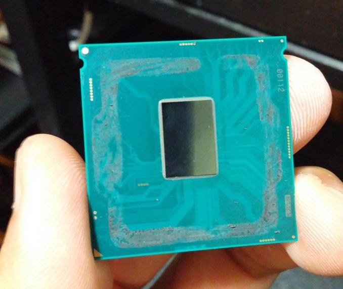
Image from Splave
CPU Specification Comparison CPU Process
NodeCores GPU Transistor
Count
(Schematic)Die Size Intel Skylake GT2 4C 14nm 4 GT2 ? 122.4mm2 Intel Broadwell-H GT3e 4C 14nm 4 GT3e ? ? Intel Haswell-E 8C 22nm 8 N/A 2.6B 356mm2 Intel Haswell GT2 4C 22nm 4 GT2 1.4B 177mm2 Intel Haswell ULT GT3 2C 22nm 2 GT3 1.3B 181mm2 Intel Ivy Bridge-E 6C 22nm 6 N/A 1.86B 257mm2 Intel Ivy Bridge 4C 22nm 4 GT2 1.2B 160mm2 Intel Sandy Bridge-E 6C 32nm 6 N/A 2.27B 435mm2 Intel Sandy Bridge 4C 32nm 4 GT2 995M 216mm2 Intel Lynnfield 4C 45nm 4 N/A 774M 296mm2 AMD Trinity 4C 32nm 4 7660D 1.303B 246mm2 AMD Vishera 8C 32nm 8 N/A 1.2B 315mm2 This makes Skylake the smallest die size for a quad core desktop processor from Intel we have seen, and that is including the integrated graphics in that calcualtion. Depending on the exact architectural details, previously in Haswell the die area was a near even split for cores and graphics after the L3 cache and IO functions (PCIe, Memory, DMI) were removed.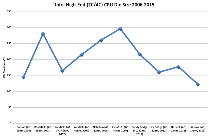
We won't know exact transistor numbers until they are disclosed at Intel's Developer Forum in mid-August, as well as a false color image die shot to show how much die area the main parts of the architecture are using. Although given the similarity to Haswell in terms of feature set (it seems to be similar with a few minor additions such as fixed function units, slightly different libraries, dual memory channels, DMI 3.0, etc.), if we take the number of transistors that GT2 Haswell had (1.4 billion) and put them in the die area we measure from the image, this comes out to a 11.4 million transistors per mm2.
Die size aside, Skylake also has a substantially thinner package than Devil's Canyon:
According to PCWatch, the package thickness of the Core i7-4770K is 1.1mm, compared to 0.8mm for Skylake. This is a direct result of using fewer PCB layers, and here we count five for Skylake and eight for Haswell.
Image from Splave
Image from PCWatch
There could eye several reasons for this. The removal of the fully integrated voltage regulator (FIVR) might reduce the number of PCB layers for power planes. The nature of the 14nm die might facilitate a thinner package as well. The cynical answer is that it is used to drive down cost. In the motherboard industry, a PCB with more layers is substantially more expensive but simplifies design when there are more features - there's also a side argument if more layers or fewer layers is better for overclocking. If we transplant this thinking to the processor, it becomes a balance of cost vs. complexity. Either way, the retail price of the processor is still relatively consistent with the previous iterations. Another thought to add to the mix would be if Intel has plans in the works to launch higher end processors based on Skylake (Kaby Lake?) in the future. The slight change in Intel's processor naming scheme (4770K to 6700K, as in 70K to 00K) also points to the potential move later in the lifetime of the product. The only hint in the naming scheme from Intel is that the 'processor numbering reflects that these processors belong to the 6th Gen Intel Core family'.
The thinness of the package has implications for removing the lid/heatspreader of the processor as well. Splave notes that previous heatspreader methods involving force, such as vices that were common during Haswell's tenure, may not be appropriate due to the thinness of Skylake. Splave shows an image of a failed attempt by another user on a Skylake CPU:
Instead, a razor method (and something warm such as a hairdryer or the bean bags that iFixit uses to warm up glue in smartphones to take them apart) to cut through the black adhesive between the package and the IHS is suggested and it what was used for the CPU above. As there are no FIVR resistors to worry about on the top of the package, the first resistance a razor blade will encounter after the black adhesive is the silicon dye itself. All that being said, over at PCWatch they successfully have used a vice method.
Image from Splave
Interestingly the heatspreader for Skylake is heavier than that from Haswell by nearly 20%, moving up from 22g to 26g. Given the copper mass that usually sits on a high end processor this should not matter much, although basic aluminium coolers might see a small benefit here by virtue of the minor extra mass.
Image from Splave
So why are we talking about removing the heatspreader? Back with Haswell (as well as Ivy Bridge to a degree), it was discovered that the thermal interface material between the silicon die and the heatspreader was both an insufficient amount and lower quality than previous generations, as well as the heatspreader being far away from the CPU due to the black adhesive, causing more air bubbles and poorer heat transfer than is optimal. For a stock processor, this difference has little effect to the use of the system, but for overclockers it meant that they were more thermally limited than silicon limited with their overclocking.
Devil's Canyon changed that - here was a better binned Haswell processor with a higher quality package, giving a ten degrees cooler system at load. It is worth noting that previously on certain platforms Intel had been providing a mixed metal interface (generalized as a soldered interface) between the silicon and the heatspreader, which is the best but most expensive option. If the cost of the interface is reduced by 0.1 cents, then that's a significant saving on millions of processors. Devil's Canyon was a small subset of sales, so spending that extra for that specific crowd could be seen as beneficial to Intel's perspective by overclockers.
Image courtesy of Idontcare
To paraphrase Splave again, he comments that the thermal paste on his Skylake is certainly worse than that of Devil's Canyon. By replacing his own thermal paste and resecuring the heatspreader, he saw an 18°C drop in temperatures at his highest air overclock with the old paste (5.1 GHz at 1.48 volts) - from 96ºC that overheated to 78ºC on the warmest core. An 18°C drop is immense. Under those conditions, and based on rough testing not published in our Skylake review, it could equal another 100-400 MHz depending on the quality of the processor. PCWatch confirms that switching out the paste with CoolLaboratory’s Liquid Pro (a liquid metal adhesion interface) reduced temperatures at 4.6 GHz from 88ºC to 68ºC
Image from PCWatch
This throws up some questions - is this just a result of design decisions for cost, or is there a Devil's Canyon type processor coming later in the design cycle?
Image from PCWatch
Source: Overclock.net, PCWatch
More...
-
08-10-15, 08:03 AM #5235
Anandtech: ASRock Rack C2750D4I and U-NAS NSC-800: A DIY File Server
Small businesses and power users often need the flexibility offered by a file server when compared to a dedicated NAS. This is where storage servers based on Microsoft's Windows Server offerings and systems based on Red Hat or Ubuntu Linux distributions come into play. These servers can be bought as an appliance or assembled in a do-it-yourself (DIY) fashion. Today, we will be looking at the latter approach using as ASRock Rack C2750D4I Intel Avoton mITX motherboard in a 8-bay U-NAS NSC-800 chassis.
More...
-
08-10-15, 09:00 AM #5236
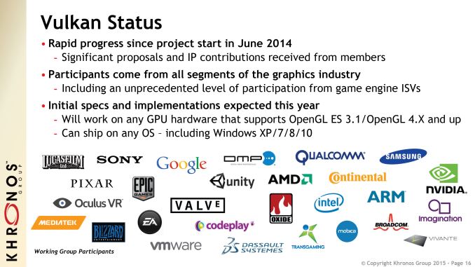
Anandtech: Vulkan Status Update: Will Use Feature Sets, Android Support Incoming
Along with updates on OpenGL, Khronos is also offering a status update on the development of Vulkan at this year’s SIGGRAPH show. Khronos’s next-generation low-level API was announced last year, with further development taking off this year when it was announced at the API would be absorbing Mantle 1.0 and would operate under its current fiery name. The API is still in development, but Khronos has a few new pieces of information to share on the progress of development.
Vulkan Feature Sets
First and foremost, there has been a bit of speculation over how Vulkan would manage being a low-level API for both mobile and desktops, and Khronos is finally answering those questions. In the OpenGL ecosystem, new features would be exposed as optional extensions, and then standardized through core releases (e.g. OpenGL ES 3.2). Due to the factors that resulted in the creation of OpenGL ES, this was never a huge problem for either branch of OpenGL since each could be scoped as appropriate and integrated separately. However with Vulkan there is now just one API, and such a coarse approach would imply limiting Vulkan to just the features mobile GPUs could support, or making even more extensive use of extensions.
To that end, today Khronos is announcing that Vulkan will support defined feature sets in order to help simplify application development and to more readily support mobile and desktop hardware under the same API. Feature sets, as implied by the name, will be groupings of features that will be advertised under a single feature set name, with the idea being that developers will build their programs against a handful of feature sets instead of a massive combination of individual extensions or capability bits (though developers can still use individual features if they’d like). Feature sets are nothing new to desktop graphics, with Microsoft’s DirectX standard having supported them since DirectX 11 in 2009.
While Khronos is announcing that Vulkan will support feature sets, they are not announcing the individual feature sets, and for good reason. In traditional Khronos consortium fashion, Khronos is going to leave the feature set definitions up to the platform holder rather than define those sets themselves. This means that it will typically be the OS developer defining the feature sets, as will be the case on Android. However because Khronos is leaving this up to the platform holder, for holders who opt not to define feature sets for their Vulkan-enabled platforms, Khronos will step in and define those feature sets. In other words platform holders get first dibs, but either way someone will take on the task of defining the feature sets.
Practically speaking, this means that while Android’s feature set will be defined by Google and one can expect SteamOS’s to be defined by Valve, Windows’ feature set will be defined by Khronos. Microsoft is a member of the Khronos consortium and could define it, however Microsoft has taken a hands-off approach on Khronos’s graphics APIs in recent years – presumably in favor of focusing on DirectX – so we’re not expecting to see Microsoft make those definitions. Feature definitions have always been a weak point of the Khronos consortium structure, so giving platform holders the right of first refusal will allow holders such as Google to break the deadlock of the consortium and dictate what features will be supported on Android. Otherwise Khronos will be able to get the job done, though one would expect not without the traditional politics of the consortium.
Android SupportVulkan Feature Set Definitions Platform Expected To Be Defined By Android Platform Holder - Google SteamOS Platform Holder - Valve? Linux Khronos? Windows Khronos (Platform holder Microsoft is anticipated to decline)
Speaking of Android, along with announcing their support for OpenGL ES 3.2 today, Google is also announcing that they will be supporting Vulkan in a future release of Android. As with OpenGL ES 3.2, no specific timeline or version of Android is mentioned, though it’s a safe bet that it will be the 2016 release. Android has traditionally heavily relied on OpenGL ES, and with Google sewing further ties with Khronos with the Android Extension Pack, it’s not surprising that Android will include support for Vulkan in order to bring low-level graphics programming to the ecosystem’s developers.
Apple, for what it’s worth, has been absent from the Khronos announcements. As the company is pushing Metal on both mobile and desktop, it looks unlikely that they will be adopting Vulkan any time soon. In which case Vulkan wouldn’t quite match OpenGL ES 3.0’s universal reach due to Apple’s reliance on proprietary APIs.
Vulkan Conformance Tests Will Be Open Source
Meanwhile on the testing and validation front, Khronos is announcing that they are teaming up with Google and the Android Open Source Project to release the Vulkan conformance tests as as open source tests. The tests themselves are being developed by Khronos members and contractors, with the Khronos/ASOP connection coming in to provide the frameworks. The tests themselves are portable to other platforms – Khronos made this point very clear in our briefing – but partnering up with Google helps Khronos get the tests out there sooner and to fulfil their open source goals.
ETA: Late 2015
Finally, Khronos is also offering a bit more guidance on when to expect the first revision of Vulkan. Khronos’s goal for the specification is to release it by the end of the year, which means they should be wrapping up development of the specification soon. Meanwhile driver/runtime development has been occurring concurrently with the development of the specification, which means that the first drivers will be ready at the same time. Khronos does require that there are working implementations before a specification is released to production, so with any luck Vulkan will be ready as a development target and for early end-user testing by the end of 2015.
More...
-
08-10-15, 10:30 AM #5237
Anandtech: Google Redesigns Hangouts for Android With Version 4.0
Today Google shipped a major update to their Hangouts application for Android. Ever since Hangouts for iOS was updated to 4.0 a little over a month ago Android users have been waiting for the update to make its way to Android. This update has been in the pipeline for quite some time, and it comes with a comprehensive redesign that brings the Hangouts app in line with Google's Material Design visual guidelines.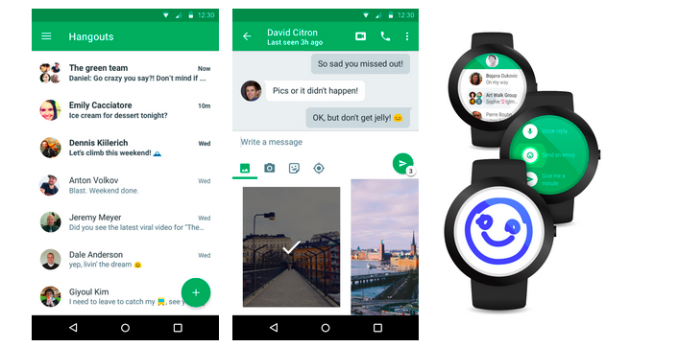
Visually, Hangouts 4.0 for Android is very similar to what shipped on iOS a little while ago. This isn't surprising, as Google's applications for iOS use their Material Design principles heavily. There are a few small differences, such as the spacing of the quick access buttons underneath the message input field, and the calling controls not being hidden behind the three dot overflow menu, but the overall appearance is the same. The appearance is definitely a departure from the previous design which had a strange dual list design which was separated into two tabs.
On top of the redesign, Google claims that Hangouts 4.0 has noticeable improvements to performance, reliability, and battery consumption. I personally have never had many issues with Hangouts on Android, but any improvements to performance are always welcomed.
Hangouts 4.0 is currently rolling out in stages, and users can expect to receive the update in the near future if they haven't already.
More...
-
08-10-15, 02:00 PM #5238
Anandtech: OpenGL @ SIGGRAPH 2015: OpenGL ES 3.2 & OpenGL Extensions Announced
Kicking off this week in Los Angeles is SIGGRAPH 2015, the computer graphics industry’s annual professional conference. As the biggest graphics event of the year this show has become the Khronos Group’s favorite venue for delivering news about the state and development of OpenGL, and this year’s show is no exception. This week will see Khronos delivering news on both OpenGL and OpenGL ES, along with the formation of the OpenGL SC 2.0 working group.
OpenGL ES 3.2
Starting things off, we have the announcement of OpenGL ES 3.2. The latest version of OpenGL’s embedded variant is receiving a new revision this week, bringing the API up to version 3.2.
With OpenGL ES 3.2, Khronos will officially be rolling the feature set of the Android Extension Pack into the core API. Until now these features have been available as optional extensions – which Google conveniently rolled into the AEP for Android developers – as not all original GPUs capable of supporting OpenGL ES 3.1 could also support the AEP, preventing those features from being rolled into OpenGL ES core.
Via these features, OpenGL ES 3.2 will bring support for tessellation, geometry shaders, compute shaders, and ASTC texture compression in to the core OpenGL ES standard. These are major features already found in desktop GPUs for some number of years now, and these days are found in all of the major mobile GPUs as well. Of particular interest here, this means that ASTC is finally part of the OpenGL ES core standard, and while it will take some time to filter out to new OSes and devices, this finally solves the problem with the lack of a standard texture compression format in the mobile space.
Meanwhile, as Khronos likes to note in their announcement, the inclusion of these features brings mobile GPUs much closer to parity with their desktop counterparts. At this point there are very few major OpenGL 4.x class (DirectX 11) features not accounted for in mobile GPUs in some form, so the gap between mobile and desktop has been further closed. And of course this means developers can push the envelope even harder on certain classes of graphical effects – especially geometry and compute-based physics simulations – though on a smaller scale more fitting of mobile hardware.
As far as OS support goes, Khronos and Google are also announcing today that OpenGL ES 3.2 will be adopted by a future version of Android – presumably 2016’s Android release – at which point OpenGL ES 3.2 will have effectively supplanted the AEP. Meanwhile we haven’t heard anything from the Apple camp about OpenGL ES in some time. iOS never received OpenGL ES 3.1 support, and with Apple gung-ho on Metal there’s no immediate reason to believe this will change with OpenGL ES 3.2.
OpenGL SC 2.0
Along with the release of OpenGL ES 3.2, Khronos is also announcing that they are forming a working group for OpenGL SC 2.0, which will be based on OpenGL ES 3.
OpenGL SC is a little-known subset of OpenGL ES that is focused on what Khronos and its members call “safety critical” systems, such as automotive and avionics systems. OpenGL SC in turn is essentially a trimmed down version of OpenGL ES that removes some of OpenGL’s flexibility in order to allow easier driver validation and ultimately more reliable operation than what is accepted for OpenGL ES.
OpenGL SC was originally created in 2005 and based off of Open GL ES 1.0, the last fixed function version of OpenGL ES. With even time-tested hardware now well outstripping the capabilities of OpenGL SC 1.0, Khronos is forming a new working group to develop OpenGL SC 2.0. 2.0 in turn will be taking OpenGL GL ES 3.x and stripping it down in a similar manner as the original specification in order to produce a pared down version of the API that is more up to date. Khronos is looking to release OpenGL ES 2.0 in 2016.
Desktop OpenGL: No New Version, But New Extensions
Finally, on the desktop OpenGL front, Khronos will not be announcing a new version of OpenGL this year, making this the first SIGGRAPH in several years where Khronos doesn’t update their venerable graphics API. Citing that OpenGL has largely caught up with desktop hardware as of OpenGL 4.5 – and with attention no doubt split by Vulkan – the consortium is instead going to release several new extensions to unlock new features. These extensions represent features that are expected to be useful for developers and worth having under Khronos control, but are not universally supported by all desktop hardware, making their inclusion into an OpenGL core standard a thorny issue.
Of particular interest on these extensions, one of the extensions will add support for multi-threaded shader compilation in OpenGL, with the goal of cutting down on loading times on shader-heavy workloads. Improved 64-bit integer support will also be coming to OpenGL as part of this extension set; 64-bit integers are still fairly rare in graphics workloads, but with many GPUs now supporting them, there are times where the extra precision is useful. And last but not least of course, as has been the case for the last few iterations of OpenGL, there will also be extensions to enable full OpenGL ES 3.2 interoperability, primarily to support developers in creating OpenGL ES applications.
Though it is interesting to note that some of the latest GPU features as exposed by Direct3D feature level 12_1 aren’t included in the extension sets, such as conservative rasterization. Right now a lot of resources are going into developing Vulkan, and while Khronos is committed to continuing to develop OpenGL separate from Vulkan, it may be that more extensive feature additions for OpenGL will have to wait until after Vulkan is done, and/or after all three major desktop vendors support these latest features.
More...
-
08-10-15, 05:00 PM #5239
Anandtech: Google Reorganizes Into Alphabet: Sundar Pichai is CEO of Google
Today, Google announced that they will undergo reorganization to better represent the growth that the company has seen in the past few years. As a result, Google the company will be now branded as Alphabet.
The big news here is that Google the internet services company will become one subsidiary of the larger Alphabet company - and said subsidiary still operating under the name Google - with the goal of better seperating Google's core business from what are now Alphabet's more experimental, far flung ventures. Consequently this change will see current parts of Google like X labs, Calico, Life Sciences, and other ventures shifted over to Alphabet. Meanwhile web services and software like Android, Maps, and Gmail will remain under the Google brand.
Organizationally, Larry Page will remain CEO of this reorganized company, and Sergey Brin will be President. Sundar Pichai will also be CEO of the new Google. Google stock is also immediately being converted over to Alphabet stock, and going forward Alphabet will be the reporting company, however Google-the-subsidiary results will be broken down and reported as part of Alphabet's results.
Ultimately it remains to be seen what effects this will have on the Google that we’ve known for the past few years. However given that the management structure has remained relatively constant in this move I suspect that business will continue on as usual.
More...
-
08-10-15, 05:30 PM #5240
Anandtech: Qualcomm Launches Snapdragon 616, 412, and 212
Today, Qualcomm launched a set of new SoCs, namely the Snapdragon 616, 412, and 212. These are updates to the Snapdragon 615, 410, and 210 respectively.
If you were to guess that these are relatively minor updates, you’d be right. First off, the Snapdragon 616 leaves the 615 mostly unchanged, with the top clockspeed of the little cluster jumping from 1 GHz to 1.2 GHz. However it should be noted that there are iterations of the 615 with a 1.11 GHz little cluster clock as well.
Meanwhile the Snapdragon 410 to 412 upgrade is a bit bigger, with the single cluster of A53s going from 1.2 GHz to 1.4 GHz and the memory interface going from a max of 533 MHz to 600 MHz. The Snapdragon 210 to 212 upgrade on the other hand is similar to the 615 to 616 upgrade, with the single cluster of A7s going from 1.1 to 1.3 GHz and are otherwise unchanged.Qualcomm's SoC Refresh Lineup Snapdragon 616 Snapdragon 412 Snapdragon 212 Manufacturing Process 28nm LP 28nm LP 28nm LP CPU 4 x ARM Cortex A53 @ 1.7GHz
4x ARM Cortex A53 @ 1.2GHz4 x ARM Cortex A53 @ 1.4GHz 4 x ARM Cortex A7 @ 1.3GHz ISA 32/64-bit ARMv8-A 32/64-bit ARMv8-A 32-bit ARMv7 GPU Adreno 405 Adreno 306 Adreno 304 H.265 Decode Yes (1080p) Yes (720p) Yes (1080p) Memory Interface 32-bit LPDDR3-800 32-bit LPDDR2/3-600 32-bit LPDDR2/3-533 Integrated Modem 9x25 core, LTE Category 4, DC-HSPA+, DS-DA 9x25 core, LTE Category 4, DC-HSPA+, DS-DA 9x25 core, LTE Category 4, DC-HSPA+, DS-DA Integrated WiFi Qualcomm VIVE 802.11ac 1-stream Qualcomm VIVE 802.11ac 1-stream 802.11n 1-stream eMMC Interface 4.51 4.51 4.5
Overall it’s a bit unfortunate that none of these SoCs have made the move from a traditional polySiON gate oxide to a high-k metal gate process yet. However I suspect that in these lower tiers even the cost of HKMG would dramatically affect competitiveness and price.
Finally, at this point it's unclear when these new variants will begin shipping, but it’s likely that this part is sampling now. Which means that devices with these new SoCs should be available before the end of the year.
More...


 Quote
QuoteThread Information
Users Browsing this Thread
There are currently 10 users browsing this thread. (0 members and 10 guests)


Bookmarks