

Results 5,241 to 5,250 of 12094
Thread: Anandtech News
-
08-10-15, 10:30 PM #5241
Anandtech: Lenovo Launches New P50 And P70 Mobile Workstations With First Mobile Xeon
Today at the SIGGRAPH 2015 Conference and Exhibition, Lenovo unveiled some new mobile workstations. The new ThinkPad P series are aimed at high-end professionals who need a lot of compute on the go. There are two models, with the P50 being a 15.6-inch version, which is a follow-on to the W541. The larger P70 features a 17.3-inch display. Both can pack some serious specifications under the hood, starting with the processor.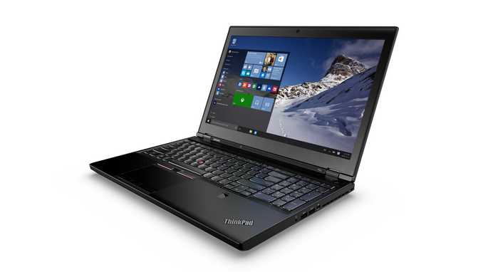
Both models will feature a new processor from Intel, which is going to be the first official mobile version of their Xeon line. Intel has not released much information yet, but the Intel Xeon E3-1500M v5 is going to be powering these workstations from Lenovo. While we don’t have exact frequencies yet, the v5 version is going to be based on the just released Skylake architecture, which brings a lot of new technology to the plate. Lenovo will offer the new P series with up to 64 GB of DDR4 memory, arranged in 4 SODIMM slots. One of the reasons to use Xeon is that it supports ECC memory, and these workstations leverage that for the workloads they will be expected to run Also part of the new Xeon will be Thunderbolt 3, and both models have this connectivity. We're not sure yet if Thunderbolt is built into the Xeons, or if something like the Aipine Ridge as an IO controller for this.
On the GPU side, Lenovo has included a Quadro card, however the exact model is not known yet.
There is also up to 1 TB of PCIe SSD storage available, and up to a 2 TB hard drive. In addition to the Thunderbolt, there will also be HDMI 1.4, mini DisplayPort 1.2, ExpressCard, SDXC, and of course what workstation would not have Gigabit Ethernet.
Wireless is a new card from Intel as well, with the Intel 8260 card which is an 802.11ac model, and Lenovo will be offering it with Bluetooth 4.1 and vPro as well. For those that need connectivity on the go, Lenovo is offering a Sierra EM7445 LTE-A option as well.
Other than the larger display, the P70 can also be had with a DVD-RW drive, but hopefully but the time it launches they will at least offer Blu-ray as an option.Lenovo P Series Mobile Workstations P50 P70 CPU Intel Xeon E3 1500M v5
Quad-core Skylake
~47W TDPGPU NVIDIA Quadro
Model number unknownMemory Up to 64 GB DDR4-2133 ECC Storage Up to 1TB PCIe SSD
Up to 2TB HDDDisplay 15.6" 1920x1080 IPS w/optional touch
Optional 3840x2160 IPS
X-Rite Pantone Color Correction17.3" 1920x1080 IPS w/optional touch
Optional 3840x2160 IPS
X-Rite Pantone Color CorrectionPorts USB 3.0 x 4
Mini DP 1.2
HDMI 1.4
Thunderbolt 3
Docking Connector
Smart Card Reader
ExpressCard
SDXC
HeadsetNetworking Intel 8260 Wireless-AC 802.11ac WiFi
Bluetooth 4.11
Optional vPro
Gigabit Ethernet
Sierra EM7445 4G LTE-ADimensions H: 0.96-1.02" (24.5-25.9 mm)
W: 14.86" (377.4 mm)
D: 9.93" (252.3 mm)H: 1.17-1.2" (29.9-31.5 mm)
W: 16.4" (416 mm)
D: 10.8" (275.5 mm)Weight Starting at 5.6 lbs (2.5kg) Starting at 7.6 lbs (3.4 kg) Battery Life 4 Cell 66 Whr
Optional 6 Cell 90 Whr8 Cell 96 WHr Price $1599+ $1999+
Speaking of the displays, Lenovo has packed some pretty impressive sounding displays into both models. The P series will offer a 1920x1080p as the base, with optional touch, and there is also a UHD 3840x2160 IPS offering as well. All of the panels are IPS models, and Lenovo has turned to X-Rite to offer Pantone color calibration out of the box, and over the lifetime of the device.
The P series can be had with a good choice of operating systems too, from Windows 10 Pro, Windows 8.1 Pro, or downgrade rights to Windows 7 Professional. If you need Linux for your workstation, they will also be offering Ubuntu and RHEL.
Gallery: Lenovo P Series


These MIL-SPEC tested and ISV Certified professional workstations will be available in Q4 2015 with the P50 starting at $1599, and the P70 starting at $1999.
Source: Lenovo
More...
-
08-11-15, 01:30 AM #5242
Anandtech: Toshiba Announces Three New NVMe SSD Families
On the eve of Flash Memory Summit (August 11-13), Toshiba has announced a full range of NVMe-based PCIe SSDs using Toshiba controllers and Toshiba MLC flash.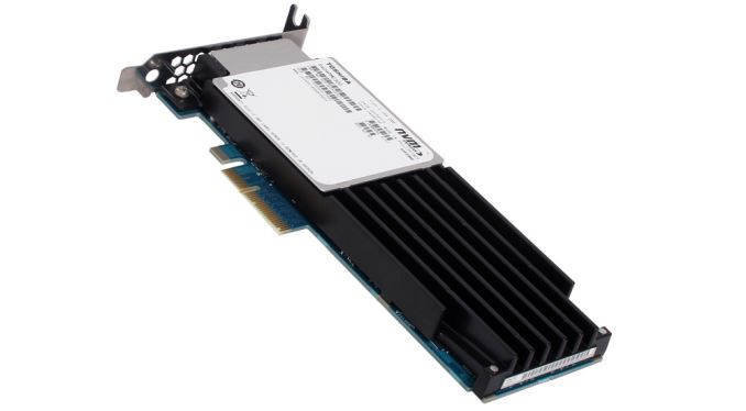
For the enterprise market, the PX04P series complements the SAS-based PX04S drives announced last week. The PX04P is available as a 2.5” drive with a U.2 (SFF-8639) connector, or as a PCIe expansion card. In either case, the drive supports four lanes of PCIe 3.0 and can make good use of that bandwidth to offer up to 3.1 GB/s sequential read speeds. With an endurance rating of 10 drive writes per day it is intended for relatively write-heavy workloads.Toshiba NVMe Drive Families Drive Series PX04P XG3 BG1 Form Factors and Interface PCIe 3.0 x4 HHHL /
2.5” U.2PCIe 3.1 x4 M.2 2280 / 2.5” SATA Express M.2 2230 /
16mm*20mm soldered module "M.2 1620"Capacities 800 GB, 1600 GB, 3200 GB Up to 1024GB Up to 256 GB QSBC Error Correction Yes Yes No TCG Pyrite Security No Yes Yes Sequential Read 3100 MB/s ? ? Sequential Write 2350 MB/s ? ? 4kB Random Read IOPS 660k ? ? 4kB Random Write IOPS 185k ? ?
For the high-performance client market, the XG3 is available in the M.2 2280 form factor using four lanes of PCIe 3.1, or as a 2.5” drive using the two-lane SATA Express connector. If these drives make it in to the retail channel, it means that consumers whose motherboards have a SATA Express connector but no M.2 slot will finally have an easy way to get in on the PCIe storage revolution.
For tablets and ultra-thin laptops, the BG1 is optimized for low power in very small packages. It comes as either an M.2 2230 card or a soldered-down module measuring 16mm by 20mm. The BG1's maximum capacity is only 256 GB, and given the power and size constraints it is probably not using a 4-lane PCIe connection.
The two client drive families implement support for the Trusted Computing Group Pyrite standard, a subset of TCG Opal that includes features necessary for things like secure boot but does not include encryption.
More...
-
08-11-15, 07:30 AM #5243
Anandtech: StarTech.com 8-bay USB 3.0 / eSATA Removable Hard Drive Enclosure Review
Network Attached Storage (NAS) devices have become quite popular over the last five years or so, but Direct Attached Storage (DAS) units were the go-to devices for consumers looking to store large amounts of data before that. The interfaces for these DAS units have evolved from USB 2.0 and Firewire to eSATA and nowadays, USB 3.x and Thunderbolt. What sort of performance numbers and features can we expect in a modern multi-bay DAS unit? What are the use-cases enabled by them in the modern computing ecosystem? Our review of the StarTech.com S358BU33ERM 8-bay USB 3.0 / eSATA hard drive enclosure provides some answers.
More...
-
08-11-15, 07:30 AM #5244
Anandtech: NVIDIA Announces Quadro M5000 & M4000 Video Cards, DesignWorks Software Su
Back in March at GTC 2015, NVIDIA announced the first member and flagship of their Maxwell 2 generation of Quadro cards, the Quadro M6000. Packing a fully-enabled GM200 GPU and 12GB of RAM, M6000 signaled an interesting shift from NVIDIA on the high-end of Quadro, with the company shipping what amounted to a “pure” graphics card as opposed to a jack-of-all-trades type card as they typically do at the high-end.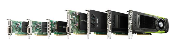
Meanwhile, although the M6000 was the first Maxwell 2 based Quadro card to launch, it was not the first Maxwell 2 GPU to launch. NVIDIA has launched GM204 and GM206 late last year and early this year respectively, and of course Maxwell 1 ended up in the Quadro K2200 and a couple of other cards. As a result we have been expecting NVIDIA to refresh the rest of the Quadro lineup with Maxwell 2 after the release of the M6000, and this week at SIGGRAPH NVIDIA is doing just that with the release of the Quadro M5000 and Quadro M4000.
We’ll start things off with the Quadro M5000. While NVIDIA has not announced the GPU for these new products, we believe the M5000 to be based on GM204, given the CUDA core and memory bus configuration. By those standards M5000 would be a fully enabled GM204 card, featuring all 2048 CUDA cores and the full 256-bit memory bus, essentially making this the Quadro version of the GeForce GTX 980.NVIDIA Quadro Specification Comparison Quadro M5000 Quadro M4000 Quadro K5200 Quadro K4200 CUDA Cores 2048 1664 2304 1344 Boost Clock ~1050MHz ~780MHz 650MHz 780MHz Memory Clock 6.6GHz GDDR5 6GHz GDDR5 6GHz GDDR5 5.4GHz GDDR5 Memory Bus Width 256-bit 256-bit 256-bit 256-bit VRAM 8GB 8GB 8GB 4GB FP64 1/32 1/32 1/24 1/24 TDP 150W 120W 150W 105W GPU GM204? GM204 GK110 GK104 Architecture Maxwell 2 Maxwell 2 Kepler Kepler Size Double-Slot Single-Slot Double-Slot Single-Slot 4Kp60 Displays Supported 4 4 2 2
Curiously, the M5000 features DRAM soft ECC support, allowing for error correction on the DRAM. Previous 5000-series Quadro cards have also included this feature, but at a GPU level NVIDIA typically reserves this feature for their highest-tier GPUs. With that said, as it’s software based and we’ve seen NVIDIA enable it in a Kepler-based GK104 product before (Tesla K10), for the moment we believe that they have gone ahead and enabled it for this GM204 product, rather than outfitting the card with GM200.
Paired up with the GM204 is 8GB of GDDR5 clocked at a slightly more conservative 6.6GHz. Based on these specifications it’s not clear whether NVIDIA is using 16 4Gbit chips or 8 8Gbit chips, as the latter are now available though still fairly rare (M6000 by comparison used 24 4Gbit chips). In any case this is the same amount of RAM as the previous Quadro K5200 shipped with, indicating that NVIDIA is targeting the same market segment as before.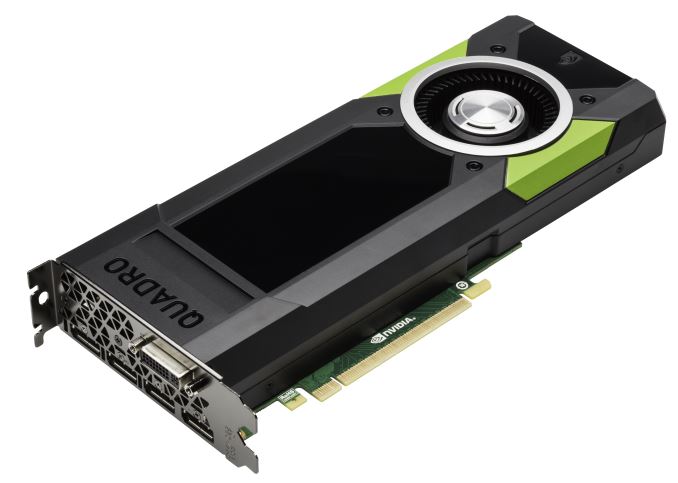
As for GPU clockspeeds, as is usually the case NVIDIA has not published specific clockspeeds, but in their press materials they have the card’s FP32 performance listed at 4.3 TFLOPs. This would put the maximum GPU clockspeeds at around 1.05GHz, though as this is a GPU boost product we don’t know the base clockspeeds at this time.
NVIDIA has also published the power information for this card, and like its Kepler-based predecessor it’s a 150W card. A 150W TDP allows M5000 to more easily work in lower power workstations where only a single 6-pin PCIe power connection is available, and is actually a bit lower power than comparable desktop GeForce products. Though as a result we expect that shipping clockspeeds are below 1GHz.
Meanwhile NVIDIA has typically gone with dual-slot blowers on their 150W Quadro cards, and M5000 will be no exception. The card is shipping with what appears to be a new blower and shroud design – and one I suspect is all plastic like the Quadro K5200’s – mimicking the original metal shroud of the M6000. At any rate this is a full size card, meaning it measures 10.5” long like NVIDIA’s other high-end cards.
Finally, much like the M6000, the overall importance of a Maxwell release is two-fold for NVIDIA. First and foremost of course are the performance improvements from Maxwell, which achieves much better performance per CUDA core and much better energy efficiency than the preceding Kepler parts, so M5000 should achieve even better real-world performance than its already substantial on-paper specifications indicate. However the other significant benefit here is that the switch to Maxwell means that the Quadro cards gain Maxwell’s newer display controller and NVENC blocks, allowing the M5000 to drive four 4K displays – twice as many as K5200 – and real-time HEVC encoding.
M4000
Also launching today and below the M5000 is the M4000. This appears to be another GM204 design, forgoing some of GM204’s CUDA cores in exchange for lower costs, performance, and power consumption. Like the M5000 we don’t have the clockspeed information for the card, but we do know it features 1664 active CUDA cores, making it analogous to the GeForce GTX 970. Also like the M5000 this features 8GB of VRAM – twice as much as the K4200 – this time clocked at 6GHz, however without the soft ECC support of the higher-end Quadro cards.
Compared to the M5000 the TDP on the M4000 is down by 30W to 120W. The previous Quadro K4200 was a 105W card, so power consumption is up slightly, but in turn the M4000 features the Maxwell family improvements and more CUDA cores than the K4200. The card is rated for 2.6 TFLOPs of FP32 performance, which puts the maximum clockspeed at around 780MHz, so we expect that performance will be greatly improved over the K4200.
Meanwhile like past Quadro 4000-series cards, the M4000 is a single slot design. To the best of our knowledge this is a new PCB design for NVIDIA, and taking advantage of the lower power requirements brings the length of the card down to 9.5”. In order to get everything down a single slot NVIDIA has done away with the DVI port – a first for the 4000 series – making M4000 a 4x DisplayPort design. As we mentioned with M5000, the Maxwel display controller improves 4K support to allow 4 such displays off of a single card, and this is a scenario NVIDIA is clearly looking to enable with the M4000.
Finally, as is usually the case for NVIDIA, the company is not publishing any official prices for these cards, leaving pricing up to their partners and vendors. That said, at this point we expect pricing to be similar to the Quadro K5200 and K4200, which would put street prices on the cards at around $2000 and $1000 for the M5000 and M4000 respectively.
NVIDIA Launches DesignWorksAlong with the release of their latest Quadro cards, NVIDIA is also announcing a new software suite at SIGGRAPH: DesignWorks. The latest Works project, DesignWorks, is partially a collection of new software and partially a branding exercise for the company. Following in the footsteps of GameWorks for game development, NVIDIA is collecting most of their tools and libraries for professional graphics development under the DesignWorks brand, and going forward will be releasing new tools under this brand as well.
Along with collecting previous disparate tools like Iray and OptiX, the announcement of DesignWorks also marks the introduction of some new tools for NVIDIA. Of particular note here is NVIDIA vMaterials, a library of digitized, real world materials for use in applications that can interface with NVIDIA’s Material Design Language, MDL. Also premiering with DesignWorks is a version of NVIDIA’s VR technology optimized specifically for professional use, aptly named DesignWorks VR.
Meanwhile NVIDIA’s technology focus for the DesignWorks launch is on Physically Based Rendering (PBR), a realistic rendering technique the company has been promoting for much of the last year now. PBR is very GPU intensive – always a plus for someone in the business of selling GPUs – but in turn is designed to offer more photo-realistic results (but not necessarily more accurate results) by focusing on simulating the properties of the materials of the surrounding world itself. This focus on PBR goes hand-in-hand with the NVIDIA vMaterials announcement in particular, as a big part of enabling PBR is creating the material representations themselves.
Finally, as part of their PBR push over the past year, NVIDIA has been showing off various images under the Real or Rendered tagline. For SIGGRAPH the company has put together an admittedly impressive render of a DeWalt drill, which is close to the real thing, though not identical to it.
Gallery: NVIDIA DesignWorks Presentation


More...
-
08-11-15, 08:31 AM #5245
Anandtech: Seagate Introduces New Nytro PCIe SSDs: XP6500 & XF/XM1440
After acquiring SSD controller designer SandForce, LSI took the quick route towards creating high-performance PCIe SSDs by putting multiple SandForce controllers and an LSI RAID controller on a single expansion card, branding the resulting product as the Nytro. This Nytro product line was transferred to Seagate along with the SandForce division in May 2014, and it's now getting both a refresh and a major expansion.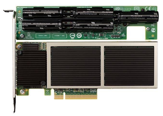
The new Nytro XP6500 succeeds the Nytro XP6302 and offers improved write latency and improved write endurance. Write throughput suffers slightly, but the XP6302's original performance specifications were inflated by testing at 28% over-provisioning rather than the default of 17% that is implied by the listed capacities. Meanwhile the XP6500 4TB model is listed as optimized for 8kB rather than 4kB random accesses, so its IOPS numbers aren't directly comparable to the others.
Peak power consumption isn't listed but is likely significantly increased over the XP6302's 39W, based on the increase in required airflow from 300LFM to 550LFM for the same operating temperature range. The Nytro XP6500 supports a supercapacitor bank to protect data in its large (2-4GB) DRAM cache. The XP6500 is available either as a full-height expansion card with built-in supercapacitors, or as a half-height card with an optional tethered supercapacitor module. Seagate has announced immediate availability of the Nytro XP6500.Seagate Nytro XP6000 Series Drive XP6500 4TB XP6500 1.5TB XP6302 Usable capacity 3.4TB 1.3TB 1.3TB, 1.75TB, 3.5TB Interface PCIe 3.0 x8 Sequential read 4 GB/s Sequential write 2.2 GB/s 1.5 GB/s 2.3 GB/s Random read IOPS 275K (8KB) 300K (4KB) 296K (4KB) Random write IOPS 85K (8KB) 100K (4KB) 148K (4KB) Write latency 14µs 33µs Write endurance 20 PB 8 PB 6.6-11.7 PB Required airflow 550 LFM 300 LFM
Expanding the Nytro brand into new territory are the XF1440 and XM1440 NVMe drives, in 2.5" U.2 (SFF-8639) and M.2 22110 form factors respectively. They're split in to two tiers: “Endurance Optimized” (3 drive writes per day) and “Capacity Optimized” (0.3 DWPD).
Seagate Nytro XF1440 Drive Endurance Optimized Capacity Optimized Usable capacity 400 GB, 800 GB, 1600 GB 480 GB, 960 GB, 1800 GB Interface PCIe 3.0 x4 SFF-8639 Sequential read 2700 MB/s Sequential write 600-1200 MB/s Random read IOPS 200K Random write IOPS 34K 3K–7K Write endurance 3 DWPD 0.3 DWPD Warranty 5 years Peak power 12.5 W Average read/write power 9 W Performance specifications for the Nytro XM1440 weren't available, and we aren't assuming that they will be the same as for the Nytro XF1440. The XF is listed as using eMLC (Enterprise MLC) but the XM is using MLC+, a term often used to refer to higher-binned consumer-grade MLC. Maximum power consumption is significantly lower for the XM, and the XM will be released later (early 2016, when the XF1440 will ship at the end of October), which suggests that there may also be controller differences.
Seagate Nytro XM1440 Drive Endurance Optimized Capacity Optimized Usable capacity 400 GB, 800 GB 480 GB, 960 GB Interface M.2 PCIe 3.0 x4 Write endurance 3 DWPD 0.3 DWPD Warranty 5 years Peak power 8.25 W Average read/write power 7 W
More...
-
08-11-15, 04:30 PM #5246
Anandtech: SanDisk Announces Second Generation CloudSpeed Ultra SATA Enterprise SSD
At Flash Memory Summit today SanDisk announced the second generation of their CloudSpeed Ultra enterprise drive. This is the sibling to the gen. 2 CloudSpeed Eco that was announced in June.
As with the Eco gen. 2, the Ultra gen. 2 transitions from 19nm to 15nm MLC and brings a reduced endurance rating but increased performance. The Ultra model continues to be geared for mixed read/write workloads while the Eco is for more read-intensive uses.
SanDisk is already supplying the CloudSpeed Ultra gen. 2 to several major customers for large-scale deployments and it will be more broadly available later in 2015, where it will be competing against drives like Samsung's SM863 and Intel's DC S3610. Pricing will be under $1/GB, but we don't know by how much. It probably won't be undercut by Intel's DC S3610, but to be competitive it will need to be down near Samsung's $0.66/GB for the SM863.SanDisk Enterprise SATA SSDs Drive Ultra gen. 2 Eco gen. 2 Ultra gen. 1 Capacities 400GB, 800GB, 1600GB 480GB, 960GB, 1920GB 100GB, 200GB, 400GB, 800GB NAND SanDisk 15nm MLC SanDisk 15nm MLC SanDisk 19nm MLC Sequential Read 530 MB/s 530 MB/s 450 MB/s Sequential Write 460 MB/s 460 MB/s 400 MB/s 4kB Random Read IOPS 76k 76k 75k 4kB Random Write IOPS 32k 14k 30k Endurance Rating 1.8 DWPD 0.6 DWPD 3 DWPD
More...
-
08-12-15, 07:31 AM #5247
Anandtech: Toshiba Brings Through-Silicon Vias to NAND Flash
At Flash Memory Summit this week, Toshiba is showing off a NAND flash device packaged using through-silicon vias rather than traditional wire-bonded connections.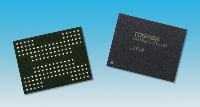
The NAND flash currently on the market is typically produced in the form of a die with a capacity like 128Gb (16GB). The popular SSD form factors don't have enough surface area to fit dozens of those chips, and SSD controllers don't have the pin count to connect to that many independently, so several chips are stacked in a single postage-stamp sized package. The traditional way of connecting the individual dies in a stack is to use the same technique as for a single-die package: bonding a thin gold wire between the edge of the die and the package substrate or external pins. The downsides are that it requires a lot of wires and the edges of the dies in the stack need to be exposed somehow, either by staggering them or by putting a spacer between each layer.
An alternative packaging method is to design the dies to participate in the stacking, by including electrical conductors that penetrate the entire thickness of the silicon die so that they can make contact with the dies above and below it in the stack, essentially tunneling right through each die. These through-silicon vias (TSVs) can then form a shared bus to carry signals from any of the dies in the stack out to the last die, which is the only one with the external connections.
Chip stacking using TSVs requires the dies to be aligned and stacked without spacers, which makes the whole stack a bit more compact. Since TSVs can be placed anywhere on the chip rather than just at the edge, it's easy to implement a wide data bus and communication within the stack can be very fast or low-power due to the short distances involved. These advantages have been very attractive for packaging DRAM, most notably in the form of the HBM stacks used by AMD's R9 Fury and R9 Nano video cards.
Toshiba's demonstration is a 16-high stack of 128Gb dies in a BGA-152 package measuring 14mm by 18mm and 1.9mm thick, and an 8-high stack that's 1.35mm thick. Those numbers are all typical even for wire-bonded stacks. The speed (1Gb/s) and operating voltages (1.2V for I/O and 1.8V core) are what we would expect from a next-generation NAND interface, but the claimed 50% power reduction is a very nice improvement for a change that leaves the flash memory cells themselves unmodified.
Toshiba hasn't said whether the dies being stacked are their current 15nm planar NAND or their forthcoming 3D NAND, nor have they said when modules using TSVs will be hitting the market. The most compelling applications would be to use TSVs to stack flash atop a controller chip in an eMMC product or atop an SoC, but the power savings would be appreciated almost everywhere. If the use of TSVs allows economically stacking more than 16 dies, it could enable a dramatic increase in the density of SSDs.
More...
-
08-12-15, 07:31 AM #5248
Anandtech: Advatronix Nimbus 400 File Server Review
Small businesses and power users often need the flexibility offered by a file server when compared to a dedicated NAS. This is where storage servers based on Microsoft's Windows Server offerings and systems based on various Linux and BSD distributions come into play. These servers can be bought as an appliance or assembled in a do-it-yourself (DIY) fashion. Today, we will be looking at a system based on the former approach - the Advatronix Nimbus 400.
More...
-
08-12-15, 09:01 AM #5249
Anandtech: Qualcomm Details the Adreno 530 GPU and ISP inside the Snapdragon 820
Snapdragon 820 is still a mystery as far as official information from Qualcomm goes. However, today Qualcomm has given a bit of insight into their upcoming SoC. While there's still no information about the CPU portion featuring Qualcomm's custom 64-bit cores known as 'Kryo', there are some details about the Adreno 510 and 530 GPUs, as well as Qualcomm's Spectra image signal processor.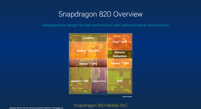
Because Adreno 530 is their new flagship GPU, Qualcomm's press release focuses more on the 530 than the 510. The performance figures released by Qualcomm describe Adreno 530 as being 40% faster than Adreno 420 on average, while also consuming 40% less power. This result is described as an average of "the top graphics benchmarks", and while it's still generally a good idea to take vendor provided numbers with a grain of salt, if the power and performance gains over Adreno 420 are anywhere in the ballpark of Qualcomm's 40% figure then Adreno 530 should end up being quite impressive.
On the API side, Adreno 500 series GPUs will support OpenGL ES 3.1 + AEP (Android Extension Pack), Renderscript, Vulkan, and OpenCL 2.0. With OpenCL 2.0 comes support for Shared Virtual Memory (SVP), which allows an OpenCL host program and a device's kernel to share a virtual address space so access to data structures like lists and trees can be easily shared between the host and GPU. Adreno 530 has varying improvements to GPGPU performance when compared to Adreno 430, but Qualcomm's slides show video processing as demonstrating the greatest improvement with a 2.5x increase in compute performance. This is also the area where efficiency gains for generational improvements typically happen, so we expect fixed-function codec support although this information is not yet provided.
As for the ISP, it's still the case that mobile image signal processors are black boxes. Qualcomm is stating that their Spectra ISP in Snapdragon 820 will be able to support 3 simultaneous cameras at up to 25MP and at 30fps with no shutter lag. The Spectra ISP will also use MIPI's higher bandwidth C-PHY serial interface, which supports the enhanced camera support. As well as this, new developer and user-facing features include support and APIs for depth maps and using dual cameras to perform refocusing or other visual effects - because Qualcomm is just the SoC manufacturer, it is up to the smartphone OEMs to implement dual-camera/depth-maps as a feature as well.
According to Qualcomm, Snapdragon 820 will start showing up in devices during the first half of 2016. Hopefully between now and then there's more information from Qualcomm about the other aspects of their new SoC, including their Kryo custom CPU core. In Q1 we will be at Mobile World Congress, so we may see more information at that time.
Source: Qualcomm, slides via Slashgear
More...
-
08-13-15, 08:01 AM #5250
Anandtech: Samsung SSD Update: 48-layer 256Gbit TLC 3D NAND & Three New TLC SSDs Anno
When Samsung took the stage at the 2015 Flash Memory Summit, they admittedly didn't deliver any bombshell announcements on the scale of the Intel/Micron 3D XPoint surprise, but they still had a lot to talk about.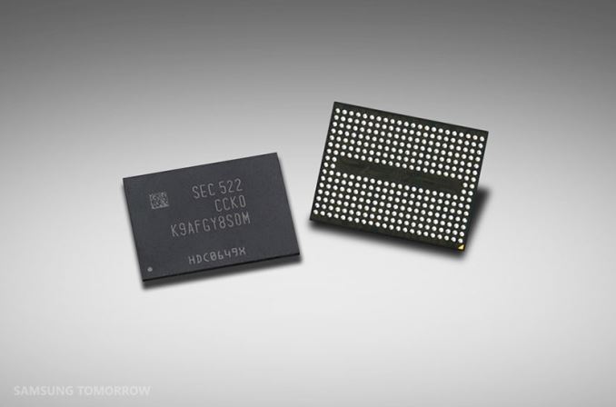
We knew that Samsung's third generation of V-NAND/3D NAND was on the way with mass production scheduled for the second half of this year. Samsung has now disclosed that mass production is starting this month, and that it's a 48-layer design with a 256Gb TLC being the first die announced. Samsung's current second-generation 3D NAND is a 32-layer design available as 128Gb TLC or 128Gb MLC.
With mass production imminent, Samsung has ensured that neither SK Hynix nor the Toshiba/SanDisk joint venture will be able to leapfrog them with their respective 48-layer 3D NAND designs, both scheduled for mass production starting in 2016.
Samsung says the new 256Gb TLC will have about 30% lower power consumption than an equivalent capacity of their current 128Gb TLC, and a switch to a dual-plane organization ensures that one 256Gb die will perform at least as well as a pair of the current 128Gb dies. Density is improved by about 40% while production costs only increased slightly, so price per GB will be going down. At FMS, Samsung is pushing the idea that their 3D NAND TLC is ready to replace MLC for most uses, and they're optimistic about scaling up their 3D NAND layer count past 100.
Samsung also shared information about three upcoming drives, all using TLC though not necessarily the new 48-layer parts. The PM1633 Enterprise SAS drive was previewed at CES in January and is intended for read-heavy workloads. A follow-on PM1633a model was mentioned to use the new 48-layer TLC to reach 15.36TB capacity, but we don't have any other information about that update. The PM953 is a general-purpose NVMe drive in M.2 or 2.5" form factors, and is the intended successor to the MLC-based SM951.New Samsung 48-Layer TLC SSDs Drive PM953 PM1633 PM1725 Form Factor NVMe over M.2 and 2.5" 2.5" SAS 12Gb/s NVMe PCIe HHHL card Capacities 480GB, 960GB, 1.92TB (2.5" only) 480GB, 960GB, 1.92TB, 3.84TB 3.2TB, 6.4TB Sequential Read ? 1,100 MB/s 5,500 MB/s Sequential Write ? 1,000 MB/s 1,800 MB/s 4kB Random Read IOPS ? 160k 1,000k 4kB Random Write IOPS ? 18k 120k Endurance Rating ? ? 5 DWPD (6.4 TB model)
Meanwhile the PM1725 is a fast multi-TB PCIe expansion card that Samsung intends to use to challenge the assumptions about what uses TLC is suited for. Relatively speaking it appears to be intended for workloads that aren't very write-heavy, but it still manages 120k IOPS for writes. That just looks small compared to 1M IOPS for reads and a sequential read speed of 5.5GB/s.
All three drives are intended for OEMs, but the PM953 will probably find its way into the retail channel just like the SM951.
Finally, along with Samsung's new 3D NAND appearing in the afformentioned new drives, it will also be appearing in at least one of their existing drives. The 850 EVO, Samsung's current consumer TLC drive, will apparently be getting an update to use the new 48-layer TLC, though it's not clear if this will be new capacities and/or a wholesale NAND update.
More...


 Quote
QuoteThread Information
Users Browsing this Thread
There are currently 23 users browsing this thread. (0 members and 23 guests)


Bookmarks