

Results 5,461 to 5,470 of 12095
Thread: Anandtech News
-
11-02-15, 09:35 AM #5461
Anandtech: AMD Announces Radeon Crimson Driver Branding & New Settings Control Panel
It was just under two months ago that AMD announced the major restructuring of their graphics division, which would see the graphics division made whole once again, more than 5 years after AMD first split it up to better align with their CPU division. Placed under the control of AMD veteran Raja Koduri, it would be the responsibility of Raja and the rest of the Radeon Technologies Group to take AMD’s GPU division in a new direction and to rebuild it after the struggles of the past half-decade.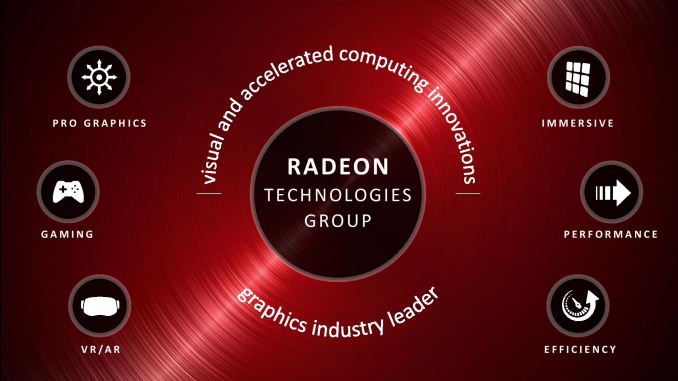
Today AMD is unveiling the first real initiative to take place under the Radeon Technologies Group banner, and that is a major rebranding of AMD’s GPU drivers and a ground-up replacement of the included control panel. At the same time, as this is the first RTG initiative, AMD and the RTG are using this occasion as their first opportunity to address the public as the Radeon Technologies Group. Typically I prefer to avoid ascribing large efforts to any one person, but in this case I think it’s safe to say that there’s a clear element of Raja making his mark on the RTG, and a desire to show how he is going to run things differently than AMD has in previous years. So for as much as today is about drivers and control panels, for the RTG today is also about the group laying out their plans for the future.
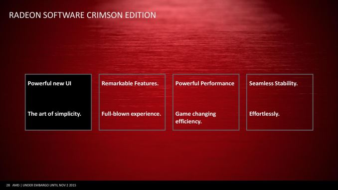
But first, let’s start with the drivers. After 13 years as the Catalyst Control Center – a name that pre-dates the AMD purchase altogether – AMD is finally doing away with the Catalyst branding. In fact, in some ways AMD is doing away with permanent driver branding altogether. Beginning with the next driver release, the Radeon drivers will be known as “Radeon Software.”
At the same time, similar to projects such as Ubuntu Linux and Android, AMD will be introducing a codename-like middle name to denote the “major version.” These names, which only fitting for the RTG will all be variations of red, will start with “Crimson Edition” and will change roughly every year as AMD introduces what they consider a new major version of the software.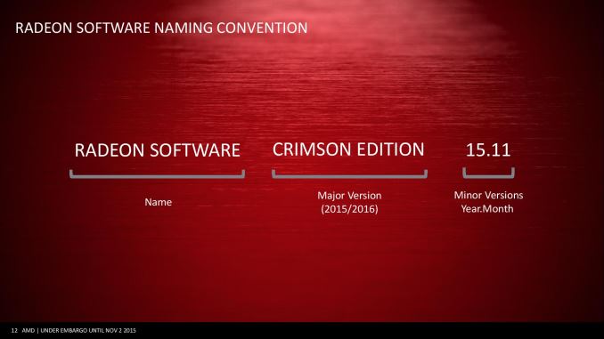
Finally, AMD will be retaining their existing year-dot-month version numbering scheme for these drivers, which will now indicate what AMD considers minor versions of the software. The end result will be that the full name of a driver release will be along the lines of “Radeon Software Crimson Edition 15.11,” which will be the name of the forthcoming November driver release.
Meanwhile, along with announcing the new name for their drivers, AMD has also clarified their driver release plans over the next year, which will be fairly similar to how things have been for the past year. AMD is aiming to find a balance on WHQL driver releases – not too many and not too few – and have told us to expect multiple WHQL releases per year, likely averaging a release every couple of months. Meanwhile in between those releases AMD will publish beta driver updates as they do now on an as-needed basis. Both AMD and NVIDIA have been wrangling with the desire to balance driver update release schedules with the need to avoid making their non-gaming customers update their drivers every two weeks, and for AMD the solution will continue to be to space out beta releases between major WHQL releases. And no, they tell us, you won’t need to register with them to download the new drivers.
Moving on, launching as part of the first Radeon Software release will be the company’s new control panel, which they are calling Radeon Settings. Radeon Settings will be a ground-up redesign for AMD, with the company ditching the entire Catalyst .NET codebase. In its place AMD has built a new control panel from scratch based on the QT framework (ed: this will only be for Windows, at least for now), with the goal of giving their control panel a rather significant visual overhaul while also addressing load time complaints that go back to the earliest days of the .NET control panel.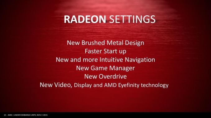
In terms of a visual style, AMD tells us that they are aiming for a much more intuitive design for Radeon Settings, and have brought in a new UI designer as part of the process. From the screenshots AMD has shared with us so far (the press was not given a preview copy ahead of today’s announcement), besides the ever-present use of brushed metal, perhaps the biggest change is that Radeon Settings is wider than it is all, and the overall style is vaguely similar to Windows Metro/Modern with a focus on large buttons as opposed to lists and drop-down menus. It is, if nothing else, much more graphical than Catalyst Control Center is.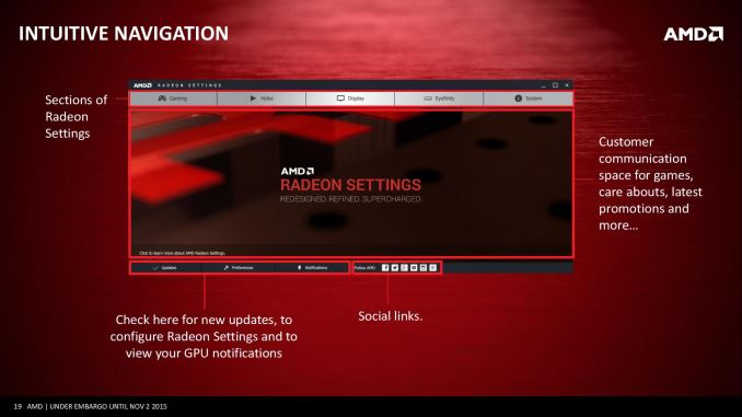
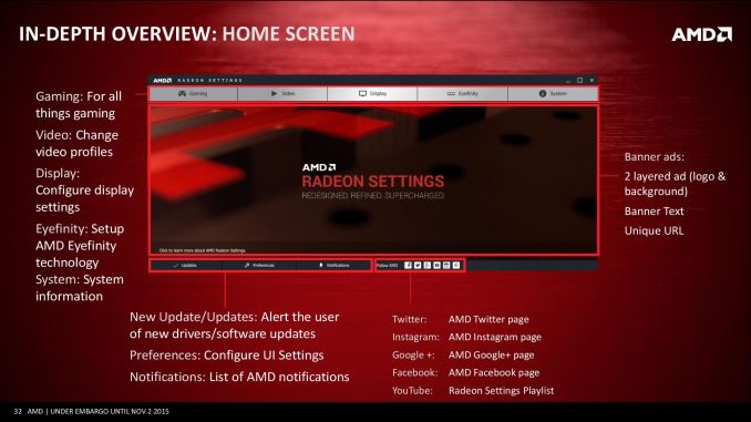
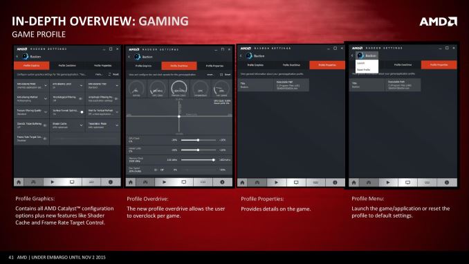
As for functionality changes, while feature updates are chiefly the domain of the drivers rather than the control panel, Radeon Settings will bring with it a couple of notable additions for gamers. Along with their existing functionality, per-game settings profiles can now contain individual settings for Crossfire, Overdrive, Framerate Target Control, and the Shader Cache, the first three features previously only being available globally and the latter being a new option entirely. Meanwhile under the Display settings, AMD is adding an Eyefinity “Quick Setup” option that will attempt a best-guess effort to arrange and enable an Eyefinity setup with a single click, allowing users to avoid the longer full setup routine when it’s not needed. Finally, after removing it a couple of years prior due to a security issue, AMD will be bringing back the driver update functionality of their control panel, allowing Radeon Settings to check for updates and to notify the user when an update is found.
At this point AMD tells us that the first release of the Radeon Software drivers and Radeon Settings control panel will be in Q4. However I expect that we may see it a bit sooner than that, and that AMD is shooting for November while offering a conservative ETA.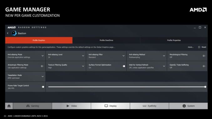
Going forward, AMD has also told us that this will be the first of multiple updates on the Radeon Software, AMD’s developer relations efforts, and the overall Radeon ecosystem. At this point AMD is setting up to execute on a multi-year plan, beginning with what the company feels is a need to be seen as being serious about software. As part of that effort the company is preparing new driver features for users, and though only briefly mentioned in passing, the new Radeon Software will ultimately bring new features for developers as well. In both cases AMD is being tight-lipped at the moment, but the messaging from the company is that they will have more to discuss on the matter later this year.
Gallery: AMD Radeon Software Crimson Slide Deck


More...
-
11-03-15, 09:36 AM #5462
Anandtech: The Crucial BX200 (480GB & 960GB) SSD Review: Crucial's First TLC NAND SSD
The Crucial BX200 is the successor to the very successful BX100 and is Crucial's new value-oriented SSD. The BX200 moves to the newer Silicon Motion SM2256 controller and is Crucial's first TLC drive, using Micron's 128Gb 16nm TLC NAND. The use of TLC will make it hard for the BX200 to achieve the BX100's combination of average performance and stellar power consumption, but it does allow for lower cost.
More...
-
11-03-15, 04:31 PM #5463
Anandtech: Microsoft Slashes OneDrive Storage Allotments
 Microsoft’s OneDrive team put up a blog post today outlining some changes coming to OneDrive, and the news is not good for pretty much anyone using the service. Just barely a year after announcing that OneDrive would offer unlimited storage for subscribers to Office 365 consumer and business, the Redmond company has decided to back out on that commitment. Here are the changes.
First, subscribers to Office 365 consumer will have their storage allotment reduced from unlimited to 1 TB. This is clearly a significant downgrade, and any users who are using more than 1 TB will be notified, and their data will be kept for “over 12 months” before it is reduced. Microsoft is attributing this to some users gobbling up excessive storage, with an example given of a single user having 75 TB of cloud storage used up. The reduction will mean that Office 365 Personal will be 1 TB, and Office 365 Home will be 1 TB for up to five people, or 5 TB total. If you are over the 1 TB limit though, tough luck. Microsoft will not be offering tiers higher than 1 TB even at an increased cost.
The bad news doesn’t stop there though. The paid 100 GB and 200 GB tiers are now gone, and have been replaced with a single 50 GB offering for $1.99 per month. So you get half the storage now for the same price. Previously the 100 GB plan was $2 per month and the 200 GB option was $4 per month. This seriously reduces the number of tiers, and you now go from free, to 50 GB, to 1 TB, with no other options anywhere else.
And, they may as well sweeten the pot with even more reductions. The free tier, which originally started at 25 GB, and was then reduced to 5 GB, and increased again to 15 GB, is once again reduced to 5 GB. They are now in-line with what Apple offers with iCloud, but Google Drive is still 15 GB for free. This is a massive reduction, and to add more salt to the wound, anyone who had been using the extra 15 GB free for using the camera roll feature of OneDrive will also have that removed.
This makes the new OneDrive look like this:
Clearly, this is a massive reduction in service for most users. Microsoft is trying to lay the blame on several users with excessive amounts of cloud storage use, but that is likely not the motivating factor. They could easily have dealt with these users on an individual basis without the massive reductions in service, and paid users abusing the paid system should not affect the free system.Microsoft OneDrive Storage Allotments Free Tier Paid Tier 1 Paid Tier 2 Office 365 Consumer Current Allotment 15 GB + 15 GB Camera Roll 100 GB for $2/month 200 GB for $4/month Unlimited Storage New Allotment 5 GB 50 GB for $2/month No second tier 1 TB
There is more information in the blog post which I would guess was posted accidentally. Microsoft says that the 75 TB user was using “14,000 times the average” which means that the average allotment of OneDrive use is just 5 GB of storage, despite paying for unlimited.
So there are a lot of use cases to be addressed. As I already mentioned, if you are over 1 TB of OneDrive, you will be notified and your data will be kept for at least 12 months before it is cleared out. If OneDrive is no longer what you want to use, you can apply for a pro-rated refund of your subscription. If you are currently subscribing to the 100 GB and 200 GB plans, there are no changes, and any changes will only affect new subscribers. If you are using the free tier, and are over the 5 GB limit that will be imposed, you will receive a free year of Office 365 personal and the 1 TB allotment that comes with it, assuming you provide a credit card. If you don’t want to provide a credit card, your data will be kept for at least 12 months as well.
Microsoft is going to implement these changes in early 2016. OneDrive is still one of the best prices for 1 TB, but these kinds of wholesale changes to the product are going to have ripple effects for some time to come. If you were using just the free tier, there are certainly other solutions which offer more storage at no cost now.
Source: OneDrive Blog
More...
-
11-04-15, 07:37 AM #5464
Anandtech: The G.Skill KM780 Mechanical Keyboard & MX780 Gaming Mouse Review
G.Skill is entering the gaming peripherals market with a new mechanical gaming keyboard and a laser gaming mouse. The KM780 is the first keyboard with Cherry MX RGB switches that we see after Corsair's exclusive use of them in 2014, while the MX780 combines high performance features with an ambidextrous design.
More...
-
11-04-15, 01:38 PM #5465
Anandtech: Build-A-Rig Round 2, SilverStone vs Crucial: The $800 PC Build Logs
After starting our second Build-A-Rig project a couple of weeks ago the build logs are in and we can see what it is like to work hands on with the hardware selected by SilverStone's Tony Ou and Crucial's Jeremy Mortensen. Build-A-Rig allows us at AnandTech, with the help of Newegg, to create builds with the parts picked by industry members. Aside from a budget and target use case there are no other restrictions on what each company can do with their build.
With parts list in hand we interviewed both Tony and Jeremy, discussed their background and motives for choosing the components they did, and ran a detailed critique of all the components chosen. For our second Build-A-Rig match they were given the objective to build an $800 back to school build. SilverStone shot for a machine that slanted more toward gaming and high quality components while Crucial maintained a more balanced machine with a more potent processor and larger SSD.
More...
-
11-04-15, 05:00 PM #5466
Anandtech: NVIDIA Launches NVS 810 Digital Signage Video Card
Entry level multi-display workstations aren’t a market that gets anywhere near the amount of attention that many of us are used to seeing in other markets. Never the less it is a market that definitely needs something catering to its needs, be it large format signage, financial trading, or any other area where a large number of displays are needed but not a large amount of horsepower to push them.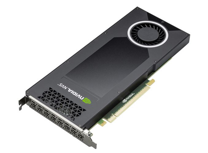
To that end, today NVIDIA is launching a new entry into their venerable NVS multi-display lineup, the NVS 810. Seeing as this market segment doesn't see updates very often this is the first and possibly only Maxwell based card to be released in this sector. This card is based around a pair of GM107 GPUs on a single board, allowing NVIDIA to outfit the NVS 810 with 8 mini-DP 1.2 ports on a single-wide PCIe card.
For the NVS 810’s hardware, under the hood we are looking at a pair of partially enabled GM107 GPUs with 512 of 640 CUDA cores enabled, for a total of 1024 CUDA cores. This is paired up with 2GB of VRAM per GPU for a total of 4GB, and though NVIDIA doesn’t specify the memory type it’s safe to assume it’s DDR3. Otherwise NVIDIA is targeting a relatively low power profile here – just 68W total board power – with the lower board power helping with GPU density and makes stuffing the maximum of four of these cards into a single machine at once a much more civil affair.
Speaking of stuffing cards in a machine, while I imagine that real world implementations of this may be rare, where I notice that this solution gets immensely crazy is the sheer number of mDP ports on hand coupled with the ability to fit four in one machine. Coupled with NVIDIA’s Mosaic display stitching and synchronization software, it’s possible to use a pair of NVS 810s together to drive up to 16 4K displays as if they are one massive display. Regardless of the rarity of such an implementation the idea that one could build a micro-ATX computer that could drive what’s functionally a 137MP display is a very impressive thought indeed.NVIDIA NVS 810 Specfications NVS 810 CUDA Cores 2 x 512 (1024) Memory 2 x 2GB (4GB) Display Connectors 8x Mini DisplayPort
(8x 4096x2160 @ 30Hz or
4x 4096x2160 @ 60Hz)Max Configuration
(Win10/Linux)4 Boards, 32 Displays Total Board Power 68W Length 9.5" Width Single Wide (4.4") Cooling Active MSRP $650-$750
Wrapping things up, NVIDIA tells us that the NVS 810 is expected to have a street price in the $650-$750 range. Overall the company is pitching the NVS 810 as a high density, low total cost solution to situations requiring a large number of high pixel count displays. As a result NVIDIA is chasing a very specific market with the board, but for those with such needs the NVS 810 brings quite a bit to the table.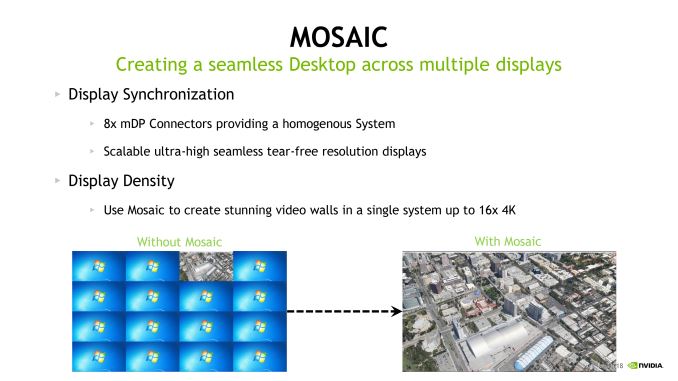
More...
-
11-05-15, 07:07 AM #5467
Anandtech: Asustor AS6204T Braswell NAS Review
Asustor is one of the recent entrants in the NAS market. Over the last couple of years, they have tried to play in the same space as QNAP and Synology, targeting power users and SMBs. They have a wide variety of hardware platforms to choose from, ranging from ARM-based 2-bay systems to Xeon-based rackmounts. Asustor launched the AS6xxx series NAS units based on Braswell SoCs in September 2015. We had the opportunity to put the AS6204T, a 4-bay model based on the quad-core Intel Celeron N3150, through our NAS evaluation routine. Read on to see how the unit stacks up against the competitors in this space.
More...
-
11-05-15, 10:31 AM #5468
Anandtech: HiSilicon Announces New Kirin 950 SoC
Today in Beijing HiSilicon held an extensive media briefing on their brand new flagship SoC - the Kirin 950. The new chipset is a very large leap for the Huawei subsidiary as it represents the first true flagship successor to the Kirin 920 that we've seen a little over a year ago in the Honor 6 review.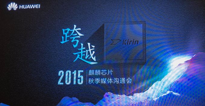
In the past we're been quite disappointed with the Kirin's overall performance in phones such as the Mate 7 or the new P8. The reason to this was mostly due to lacklustre showing of the GPU and general low efficiency of the SoC. The new chipsets promises to bring a lot of improvements and also represents a lot of firsts for the company, so let's immediately go over the configuration details of the SoC.
In terms of CPU HiSilicon continues the usage of a traditional big.LITTLE setup with four Cortex A72 and four A53 cores. This effectively makes HiSilicon the second vendor after MediaTek to ship ARM's new CPU core and the first one to do so in a mobile device. Thanks to the new process node the big core's frequency is able to be pushed up to 2.3GHz while the little cores clock in at up to 1.8GHz. HiSilicon estimates that the A72 is overall 11% faster clock-for-clock than current A57 designs, so together with the slightly higher clocks we should see the Kirin 950 perform about 20% better than the Exynos 7420 in CPU-bound tasks.HiSilicon High-End Kirin Lineup SoC Kirin 920/925 Kirin 930/935 Kirin 950 CPU 4x Cortex A15@1.7/1.8GHz
4x Cortex A7@1.3GHz4x Cortex A53 @2.0/2.2GHz
4x Cortex A53 @1.5GHz4x Cortex A72 @2.3GHz
4x Cortex A53@1.8GHzMemory
Controller2x 32-bit @ 800MHz
LPDDR3
12.8GB/s b/w2x 32-bit @ 800MHzLPDDR3
12.8GB/s b/w2x 32-bit
LPDDR3 or LPDDR4GPU Mali T628MP4 @ 600MHz Mali T628MP4 @ 680MHzMali T880MP4 @ 900MHzEncode/
Decode1080p H.264
Decode & Encode1080p H.264
Decode & Encode1080p H.264Decode & Encode
2160p30 HEVC
DecodeCamera/ISP Bad one Dual 14bit ISP
940MP/sIntegrated
ModemBalong Integrated
UE Cat. 6 LTE
On the GPU side, the Kirin 950 gets an upgrade to Mali's new T880 GPU, again making this the first silicon implementation of the new ARM IP. The designers chose to remain with an MP4 configuration, but with a vastly increased clock rate of to up to 900MHz. I asked the company's senior planning manager as to why they chose to go with a lower core count and high frequency over a potentially more power efficient wider implementation at lower clock speeds, and the answer seems to be strikingly similar to MediaTek's explanation to the same question;
For the very vast majority of use-cases and users the GPU isn't a bottleneck and the full potential of more powerful GPUs are never utilized, so the vendors prefer to save die space and thus cost by using less GPU cores. As such, while the upgrade represents a significant improvement over previous Kirin chipsets, one shouldn't expect it to compete with more powerful alternatives such as from Qualcomm or Samsung.
Due to the new SoC having both A72 CPU cores and the new T880 Mali GPU I was expecting it to also ship with ARM's new CCI-500 - after all, all 3 IPs were launched simultaenously back in February. Unfortunately HiSilicon explained that the new interconnect wasn't ready during the Kirin 950's design phase and thus the designers had to rely on the older CCI-400 that has been used in all big.LITTLE SoCs released to date.
HiSilicon claims to have made some significant leaps in terms of ISP and DSP performance. In fact, the Kirin 950 is the first SoC that uses their newly developed PrimISP and IVP32 DSP. The new IP arose out of the 2013 aquisition of Texas Instrument's OMAP SoC operations in Nice, France. The subsequent founding of Huawei's Image Technology R&D Center allowed the company to have the design resources to build products tailored to their needs. As such, Huawei is finally able to sport a cutting-edge and competitive ISP/DSP integrated in the SoC which in the future will be able avoid usage of dedicated external ISP's such as those employed in this year's Huawei devices such as the Honor 6+, P8 or Mate S.
On the multimedia side, the company did not talk much about its encode and decode capabilities, and it seems the reason for that is that they're not that impressive to talk about. While the new SoC can now decode HEVC at up to 4K resolution at 30fps, the encode capabilities have not evolved from the previous generation and thus is limited to 1080p30 H264. This also means that while the ISP would be able to handle 4K video, the actual encoder would make it impossible to actually implement 4K recording on a device product.
In terms of memory subsystem, the SoC is the first in the mobile industry to employ a hybrid LPDDR3 / LPDDR4 memory controller. It was only last week that ARM had announced a similar IP in the form of the DMC-500, but HiSilicon explained that the block employed in the Kirin 950 is of their own design and they were very proud to be able to offer this capability ahead of the competition.
In terms of connectivity, the SoC still employs an integrated Balong modem capable of 5-mode UE Category 6 LTE speeds of up to 300Mbps. There wasn't much talk about the modem so likely the improvements were kept relatively minor.
Lastly, we saw an upgrade to the SoC's sensor-hub. The new i5 succeeds the i3 used in the Kirin 92X and 930's. The new co-processor is powered by an ARM Cortex M7 core which is able to provide much more processing performance at much lower power.
TSMC 16FF+ Manufactured
As mentioned earlier, the Kirin 950 is HiSilicon's first TSMC 16FF+ manufactured mobile SoC. This also makes the Chinese vendor second in line after Apple's to release mobile silicon based on the new manufacturing node.
In fact, HiSilicon explains that along with Apple they've been the two main lead partners of the Taiwanese semiconductor giant, and both parties have been working closely together to try to improve the design and to tune the process. In fact, the company revealed that first mass production (also commonly named as risk production) started as early as last January. Over the following months both companies cooperated to sort out bugs and imperfections in the design (chip revisions) to go up from 20% yield in the earliest runs to up to 80% yields and qualified mass production this last August.
HiSilicon was stressing in particular one aspect of the new process: reduced power density. Over the last few years we've seen semiconductor manufacturers able continuously shrink their process geometry, but power consumption reductions were not able to scale at the same pace. The result is that with each new generation, even if total TDP might have been kept the same, the actual power density on the silicon has gone up significantly. This causes problems with thermal dissipation and can lead to hot-spots on the silicon die which then exceed the safe operating temperatures of the chipset. Until now vendors would circumvent this problem by creating "dark silicon", meaning silicon area on the die in which there is no logic and only serves as "padding" to help thermal dissipation.
HiSilicon explains that TSMC's 20SoC node in particular had seen the negative effects of this development as the power density went up 42.5% over the previous 28HPM node. The introduction of FinFETs in the new 16FF+ is able to drastically improve this metric by more than halving the power density compared to the 20SoC process. The company was especially enthusiastic when talking about this improvement and emphasising the severity of the issue that this has caused in the past. One visible impact of this seems to be the CPU's block sizes, as we're seeing a much smaller big cluster than we would normally expect.
The company was able to show off the implementation area of both an A57 and an A72 on 16FF+. The more interesting number which we can use in an apples-to-apples comparison and put dark silicon into perspective are the A57 figures. Here HiSilicon claims that it an A57 implementation takes up around 9.7mm² - much less than the 13.2 and 15.3mm² we've seen from 20SoC vendors such as Nvidia on the X1 or Qualcomm on the S810 - the point here being that the implementation is much smaller than what the ~8-10% process shrink allows.
Of course, the Kirin 950 uses the more efficient A72 cores which are able to architecturally reduce the block's footprint. As such, the Kirin's big CPU cluster comes in at only 8.0mm², beating the Exynos's 7420 8.88mm² even though Samsung has an advantage on process density.
In terms of power consumption, they also had a slide up demonstrating the power curves of the cores:
According to the graphic, the A53's max out at around 200mW while the A72's go up to ~1450mW. On the big cores this is somewhat comparable to the Exynos 7420 even though the figures we publish use a different measurement methodology and test-case. HiSilicon uses Dhrystone which I found to use about 10% more power than the power virus which I use for our deep dive power measurement articles.
The company had live development demo boards running at the event. While we were unfortunately unable to have more time with them, it does demonstrate the high maturity of the SoC. In fact, we should be seeing products in consumer's hands before the end of the year.
All in all, I think HiSilicon was able to showcase some very significant improvements to the Kirin lineup. I see the Kirin 950 as the true successor to the 920, and it seems that we'll be finally able to move forward in terms of performance and efficiency. While the Kirin still has some rough edges, especially in the aspect of media capabilities, it promises to patch up a lot of the issues that seems to have plagued Huawei's latest flagships. I'm looking forward to getting to test incoming devices with the SoC to see where it places on the competitive landscape!
More...
-
11-05-15, 08:30 PM #5469
Anandtech: GlobalFoundries and AMD Announce First 14nm FinFET Sample Production Succe
GlobalFoundries, AMD’s former chip manufacturing arm, is a fab that has seen some hard times. After being spun-off from AMD in 2009, the company has encountered repeated trouble releasing new manufacturing nodes in a timely process, culminating in the company canceling their internally developed 14XM FinFET process. Charting a new course, the in 2014 the company opted to license Samsung’s 14nm FinFET process, and in some well-needed good news for the company, today they and AMD are announcing that they have successfully fabbed AMD’s first 14nm sample chip.
Today’s announcement, which comes way of AMD, notes that the fab has produced their first 14nm FinFET LPP sample for AMD. The overall nature of the announcement is somewhat vague – GlobalFoundries isn’t really defining what “successful” means – though presumably this means AMD has recieved working samples back from the fab. Overall the message from the two companies is clear that they are making progress on bringing up 14nm manufacturing at GlobalFoundries ahead of mass production in 2016.
Of particular importance in today’s announcement is the node being used; the sample chips were fabbed on 14nm Low Power Plus (LPP), which is Samsung’s (and now GlobalFoundries’) second-generation 14nm FinFET design. Relative to the earlier 14nm Low Power Early (14LPE) design, 14LPP is a refined process designed to offer roughly 10% better performance, and going forward will be the process we expect all newer chips to be produced on. So in the long-run, this will be GlobalFoundries’ principle FinFET process.
AMD for their part has already announced that they have taped out several 14LPP designs for GlobalFondries, so a good deal of their future success hinges on their long-time partner bringing 14LPP to market in a timely manner. For today’s announcement AMD is not disclosing what chip was successfully fabbed, so it’s not clear if this was CPU, APU, or GPU, though with GlobalFoundries a CPU/APU is more likely. Though no matter what the chip, this is a welcome development for AMD; as we have seen time and time again with chips from Intel, Samsung, and Apple, a properly implemented FinFET design can significantly cut down on leakage and boost the power/performance curve, which will help AMD become more competitive with their already FinFET-enabled competition.
Samsung Brochure on 14LPE vs. 14LPP
Finally, looking at the expected timetables, GlobalFoundries’ production plans call for their 14LPP process to enter the early ramp-up phase this quarter, with full-scale production starting in 2016. Similarly, in today’s announcement AMD reiterated that they will be releasing products in 2016 based on GlobalFoundries’ 14LPP process.
More...
-
11-05-15, 09:32 PM #5470
Anandtech: NVIDIA Announces Record Revenue for Q3 FY 2016
Today NVIDIA announced their earnings for the third quarter of their fiscal year 2016 (yes their fiscal year is almost a full year ahead of calendar) and the company posted record revenues for this quarter at $1.305 billion. This is up 7% from last year, and 13% from last quarter. Gross margin was 56.3%, with an operating income of $245 million and a net income of $246 million for the quarter. This resulted in diluted earnings per share of $0.44, which was up 42% year-over-year.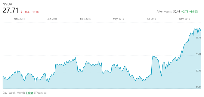
NVIDIA also reports Non-GAAP figures, which excludes stock-based compensation and acquisition costs, restructuring, and warranty. Gross margin was slightly higher at 56.5% compared to GAAP results, with operating income at $308 million and net income of $255 million. Earnings per share on a Non-GAAP basis were $0.46. The Non-GAAP numbers are important this quarter because of the large write-down NVIDIA took last quarter on their Icera modem division.NVIDIA Q3 2016 Financial Results (GAAP) Q3'2016 Q2'2016 Q3'2015 Q/Q Y/Y Revenue (in millions USD) $1305 $1153 $1225 +13% +7% Gross Margin 56.3% 55.0% 55.2% +1.3% +1.1% Operating Income (in millions USD) $245 $76 $213 +222% +15% Net Income $246 $26 $173 +846% +42% EPS $0.44 $0.05 $0.31 +780% +42%
NVIDIA saw great gains in GPU sales, which are the bulk of the company. GPU based revenue was up 12% year-over-year and up 16% over last quarter, with gaming GPU revenue up 40% over last year, and now sits at record levels. The Quadro side of the house did not fare so well, with revenues of $190 million, which is up 8% over last quarter, but down 8% compared to the same time last year. Tesla and GRID revenue was $80 million, growing since last quarter 13%, but down 8% year-over-year.NVIDIA Q3 2016 Financial Results (Non-GAAP) Q3'2016 Q2'2016 Q3'2015 Q/Q Y/Y Revenue (in millions USD) $1305 $1153 $1225 +13% +7% Gross Margin 56.5% 56.6% 55.5% -0.1% +1.0% Operating Income (in millions USD) $308 $231 $264 +33% +17% Net Income $255 $190 $220 +34% +16% EPS $0.46 $0.34 $0.39 +35% +18%
Tegra processors are still a mixed bag for NVIDIA. They have tried their hand in the mobile phone and tablet space, but with little success, but they have seen good performance from Tegra in automotive applications, and this continues to be the growth area for Tegra. For the quarter, Tegra revenue was $129 million, which is down 23% year-over-year. This decline is due to the tablet and smartphone space, because their automotive attributed revenue was $79 million, which is up 11% since last quarter and up more than 50% year-over-year. There is still hope for Tegra, but it appears to be less and less likely to be in the tablet space. NVIDIA did win the Google Pixel C tablet but it’s unclear yet how it will fare in the difficult tablet market.
NVIDIA also still receives $66 million per quarter from Intel due to a patent license agreement.
During Q3 2016, NVIDIA paid back $53 million in dividends to shareholders and bought back 4.6 million shares. Their goal for FY 2016 is to repay $800 million, and through three quarters, they are now at $604 million. NVIDIA is planning on paying approximately $1.0 billion to shareholders for their next fiscal year.NVIDIA Quarterly Revenue Comparison (GAAP) In millions Q3'2016 Q2'2016 Q3'2015 Q/Q Y/Y GPU $1110 $959 $991 +16% +12% Tegra Processor $129 $128 $168 +1% -23% Other $66 $66 $66 flat flat
Breaking down the numbers a bit more, NVIDIA has seen big growth in the gaming segment, with revenues increasing from $468 million since Q1 FY 2015 to $761 million this quarter. Year-over-year, the gaming market has grown 44%, at a time when the PC industry as a whole has contracted. PC gaming appears to be alive and well. This has covered the drop in NVIDIA’s other segments, with the biggest drop being PC & Tegra OEM, which fell from $350 million in revenue last year to just $192 million this quarter, which is a drop of 45% year-over-year. Automotive is growing, but it is still some ways away from matching the Tablet market for sales.
Overall, any time you can set a record for a quarter it is clearly good news. Not all of NVIDIA’s business is growing as quickly as they would like, but luckily for them, their largest segment is the one that is growing at a much quicker pace than the rest of the industry.
Looking ahead to next quarter, NVIDIA is expecting revenues of $1.30 billion, plus or minus 2%, with GAAP margins of 56.7%.
Source: NVIDIA Investor Relations
More...


 Quote
QuoteThread Information
Users Browsing this Thread
There are currently 26 users browsing this thread. (0 members and 26 guests)


Bookmarks