

Results 5,471 to 5,480 of 12096
Thread: Anandtech News
-
11-06-15, 07:17 AM #5471
Anandtech: The IBM POWER8 Review: Challenging the Intel Xeon
We recently got our hands on a S822L, an dual socket OpenPOWER server. IBM claims that this is an affordable, high performance and highly expandable alternative to the typical Xeon x86 Linux server. Will Intel finally have some competition in the mid range server space too? Find out as we take a look inside the server and unleash all kinds of benchmarks upon it.
More...
-
11-06-15, 11:37 AM #5472
Anandtech: Examining Intel's New Speed Shift Tech on Skylake: More Responsive Process
Modern computer processors are constantly changing their operating frequency (and voltage) depending on workload. For Intel processors, this is often handled by the operating system which will request a particular level of performance, known as the Performance State or P-State, from the processor. The processor then adjusts its frequencies and voltage levels to accomodate, in a DVFS (dynamic voltage and frequency scaling) sort of way, but only at the P-states fixed at the time of production. While the best for performance would be to run the system at the maximum all the time, due to the high voltage, this is the least efficient way to run a processor and wasteful in terms of energy used, which for mobile devices means a shorter battery life or thermal throttling. With the P-state model, to increase efficiency, the operating system can request lower P-states in order to save power, but if a task requires more performance, and the power/thermal budgets are sufficient, the P-State can be changed to accomodate. This 'technology' on Intel processors has historically been called 'Speed Step'.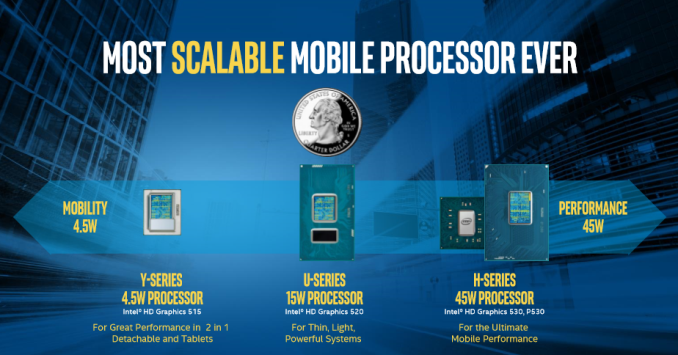
With Skylake, Intel's newest 6th generation Core processors, this changes. The processor has been designed in a way that with the right commands, the OS can hand control of the frequency and voltage back to the processor. Intel is calling this technology 'Speed Shift'. We’ve discussed Speed Shift before in Ian’s Skylake architecture analysis, but despite the in-depth talk from Intel, Speed Shift was noticably absent at the time of the launch of the processors. This is due to one of the requirements for Speed Shift - it requires operating system support to be able to hand over control of the processor performance to the CPU, and Intel had to work with Microsoft in order to get this functionality enabled in Windows 10. As of right now, anyone with a Skylake processor is actually not getting the benefit of the technology, at least right now. A patch will be rolled out in November for Windows 10 which will enable this functionality, but it is worth noting that it will take a while for it to roll out to new Windows 10 purchases.
Compared to Speed Step / P-state transitions, Intel's new Speed Shift terminology, changes the game by having the operating system relinquish some or all control of the P-States, and handing that control off to the processor. This has a couple of noticable benefits. First, it is much faster for the processor to control the ramp up and down in frequency, compared to OS control. Second, the processor has much finer control over its states, allowing it to choose the most optimum performance level for a given task, and therefore using less energy as a result. Specific jumps in frequency are reduced to around 1ms with Speed Shift's CPU control from 20-30 ms on OS control, and going from an efficient power state to maximum performance can be done in around 35 ms, compared to around 100 ms with the legacy implementation. As seen in the images below, neither technology can jump from low to high instantly, because to maintain data coherency through frequency/voltage changes there is an element of gradient as data is realigned.
The ability to quickly ramp up performance is done to increase overall responsiveness of the system, rather than linger at lower frequencies waiting for OS to pass commands through a translation layer. Speed Shift cannot increase absolute maximum performance, but on short workloads that require a brief burst of performance, it can make a big difference in how quickly that task gets done. Ultimately, much of what we do falls more into this category, such as web browsing or office work. As an example, web browsing is all about getting the page loaded quickly, and then getting the processor back down to idle.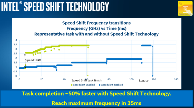
For this short piece, Intel was able to provide us with the Windows 10 patch for Speed Shift ahead of time, so that we could test and see what kind of gains it can achieve. This gives us a somewhat unique situation, since we can isolate this one variable on a new processor and measure its impact on various workloads.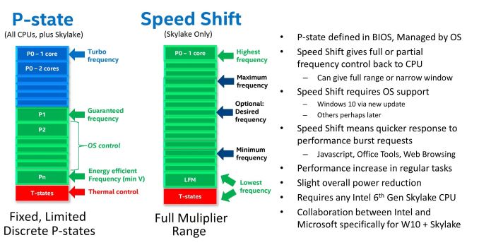
To test Speed Shift, I’ve chosen several tasks which have workloads that could show some gain from Speed Shift. Tests which run the processor at its maximum frequency for long periods of time are not going to show any significant gain, since you are not limited by the responsiveness of the processor in those cases. The first test is PCMark 8, which is a benchmark which attempts to represent real-life tasks, and the workload is not constant. In addition, I’ve run the system through several Javascript tests, which are the best case scenario for something like Speed Shift, since the processor has to quickly complete a task in order to allow you to enjoy a website.
The processor in question is an Intel Core i7-6600U, with a base frequency of 2.6 GHz, and turbo frequency of 3.4 GHz. Despite the base frequency being rated on the box at 2.6 GHz, the processor can go all the way down to 400 Mhz when idle, so being able to ramp up quickly could make a big impact even on the U-series Skylake processors. My guess is that it will be even more beneficial to the Y series Core m3/m5/m7 parts since they have a larger dynamic range, and typically more thermal constraints.
PCMark 8
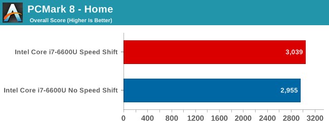 Both the Home and Work tests show a very small gain with Speed Shift enabled. The length of these benchmarks, which are between 30 and 50 minutes, would likely mask any gains on short workloads. I think this illustrates that Speed Shift is just one more tool, and not a holy grail for performance. The gain on Home is just under 3%, and the difference on the Work test is negligible.
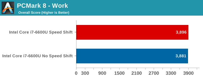
JavaScript Tests
JavaScript is one of the use cases where short burst workloads are the name of the game, and here Speed Shift has a much bigger impact. All tests were done with the Microsoft Edge browser.
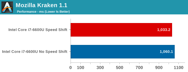

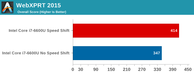 The time to complete the Kraken 1.1 test is the least affected, with just a 2.6% performance gain, but Octane's scores shows over a 4% increase. The big win here though is WebXPRT. WebXPRT includes subtests, and in particular the Photo Enhancement subtest can see up to a 50% improvement in performance. This bumps the scores up significantly, with WebXPRT 2015 showing an almost 20% score increase, and WebXPRT 2013 has a 26% gain. These leaps in performance are certainly the kind that would be noticeable to the end user manipulating photographs in something like Picasa or watching web-page based graph adjustments such as live stock feeds.
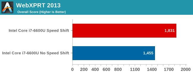
Power Consumption
The other side of the coin is power consumption. Having a processor that can quickly ramp up to its maximum frequency could mean that it will consume more power due to the greater penalty of increasing the voltage, but if it can complete the task quickly and get back to idle again, there is a chance to be more efficient when work is done in 10s of milliseconds rather than 100s of milliseconds, as the frequency ramps up and down again before the old P-state method has decided to do anything. The principle of 'work fast, finish now' was the backbone of Intel's 'Race To Sleep' strategy during the ultrabook era and focused on the impulse of response-related performance, however the drive for battery life means that efficiency has tended to matter more, especially as devices and batteries get smaller.
Due to the way modern processors work, we don’t have the tools to directly measure the SoC power. Intel has told us that Speed Shift does not impact battery life very much, one way or the other, so to verify this, I've run our light battery life test with the option disabled and enabled.
This task is likely one of the best case scenarios for Speed Shift. It consists of launching four web pages per minute, with plenty of idle time in between. Although Speed Shift seems to have a slight edge, it is very small and would fall within the margin of error on this test. Some tasks may see a slight improvement in efficiency, and others may see a slight regression, but Speed Shift is less of a power savings tool than other pieces of Skylake. Looking at it another way, if, for example, the XPS 13 with Skylake was to get 15 hours of battery life, Speed Shift would only change the result by about 7 minutes. Responsiveness increases, but net power use remains about the same.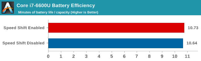
Final Words
With Skylake, while there was not the large leap in clock for clock performance gain that we have become accustomed to with new Intel microarchitectures, but when you look at the overall package, there was a decent net gain in performance combined with new technologies. For example, being able to maintain higher Turbo frequencies on multiple cores has increased the stock to stock performance more than the smaller IPC gains.
Speed Shift is just one small part of the overall performance gain, and one that we have not been able to look at until now. It does lead to some pretty big gains in task completion, if the workloads are bursty and short enough for it to make a difference. It can’t increase the absolute performance of the processor, but it can get it to maximum performance in a much shorter amount of time, as well as get it back down to idle quicker. Intel is billing it as improved responsiveness, and it’s pretty clear that they have achieved that.
The one missing link is operating system support. We’ve been told that the patch to enable this is coming to Windows 10 in November. While this short piece looks at what Speed Shift can bring to the table in terms of performance, if you'd like to read more about how it is implemented, please check out the Skylake architecture analysis which goes into more detail.
More...
-
11-09-15, 07:07 AM #5473
Anandtech: The Google Nexus 5X Review
Google's first hardware collaboration with LG brought us the Nexus 4. Like the Nexus 7, the Nexus 4 followed a philosophy of bringing as much power and quality as possible to a reasonably affordable price point. The Nexus 4 definitely wasn't a perfect phone, but it was certainly good relative to its price, and it showed that a phone can still be good even if it doesn't cost $600. About one year later Google and LG collaborated again to bring us the Nexus 5, a device which I and many other users fondly remember as an affordable phone that actually brought many of the specifications you would expect to see in a device that costed significantly more.
While I'm sure many hoped that 2014 would bring the next iteration of an LG Nexus device, it wasn't meant to be. Instead we got the Nexus 6 made by Motorola, which didn't really follow the pricing philosophy of the LG Nexus devices, and wasn't very competitive with devices like the Galaxy Note 4 despite its equivalent cost. At that point the future of affordable Nexus devices was unclear, and I wasn't even sure if we'd see a true successor to the Nexus 5. Fortunately, this year is the year that LG returns to bring us the next iteration of their Nexus phones, with the new device appropriately being named the Nexus 5X. Read on for the full review, and find out if the Nexus 5X is a worthy successor to the Nexus 5.
More...
-
11-09-15, 05:00 PM #5474
Anandtech: TAG Heuer Unveils The Intel-Powered Connected Smartwatch
Today TAG Heuer, a traditional Swiss watchmaker, announced their entry into the world of smartwatches with the TAG Heuer Connected. This is really the first example of a luxury Android wear watch, and also the first example of a traditional mechanical watch manufacturer moving into the smartwatch space.
The TAG Heuer Connected has a diameter of 46mm, a thickness of 12.8mm, and a mass of 52 grams. The chassis of the watch is made of titanium, and the LCD display is covered by a sheet of sapphire glass. The display itself is a 1.5" 360x360 fully circular transflective LTPS LCD, which means it can use the reflection of light to improve visibility and drive down power consumption. The last time I remember hearing about these sorts of displays was Pixel Qi's transflective LCDs, but the tech hasn't really gone anywhere since that time. It'll be interesting to see who is making the panel for the TAG Heuer Connected and how it fares in bright light compared to other smartwatches, as well as compared to a traditional mechanical watch which doesn't use an LCD at all.
Interestingly, the TAG Heuer connect is powered by an Intel SoC rather than the Snapdragon 400 chip that has shown up in most Android Wear devices. More specifically, it's an Intel Z34xx series SoC, which has a peak frequency of 1.6GHz but TAG Heuer notes that the nominal frequency will be more like 500MHz. The SoC is paired with 1GB of RAM and 4GB of NAND, which puts it ahead of the 512MB of RAM found in most Android Wear watches. The sensors include an accelerometer and a gyroscope, but no heart rate monitor which is definitely a letdown for fitness-oriented buyers. The watch is also advertised as having IP67 water resistance.TAG Heuer Connected SoC Intel Atom Z34xx RAM 1GB NAND 4GB Display 1.5" 360x360 LCD, 240ppi Diameter / Mass 46mm / 52g Battery 410mAh OS Android Wear Other Connectivity 802.11b/g/n + BT 4.1 Price $1499
Because 30% of the Connected's parts are made outside of Switzerland the watch isn't officially "Swiss made", and I don't expect that's going to be an easy problem to overcome when there are now many electrical parts inside the watch being made overseas. Something interesting is that the Connected is modeled off of TAG Heuer's Carrera mechanical watch, and after two years the company will allow you to trade in your Connected along with $1500 to receive an actual Carrera. To me that move seems a bit pessimistic about the company's own future in the smartwatch space, as it seems like there's an assumption that users will give up a smartwatch and go back to owning a mechanical watch. It would make more sense to me if you could trade up to newer versions of the Connected.
The last, and possibly most important detail about the TAG Heuer Connected is the price. TAG Heuer's mechanical watches can cost several hundred dollars, and so it's no surprise that the TAG Heuer Connected will have a retail price of $1500
More...
-
11-09-15, 06:05 PM #5475
Anandtech: Intel's Xeon D Product Family Updated with Storage and Networking-Specific
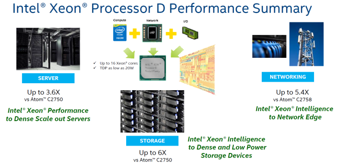
Intel's Xeon D has been one of the most exciting platforms to come out of Intel this year. Xeon D has created more excitement in the micro-server / edge server market compared to the introduction of Avoton and Rangeley (based on Silvermont x86 Atom cores) a few years back. In introducing the 22nm Atom-based server SoCs, Intel clearly delineated different SKUs for different market segments. While Avoton (C2xx0) concentrated on the storage server market, Rangeley (C2xx8) added some communication accelerators that made it a good fit for networking and communication applications.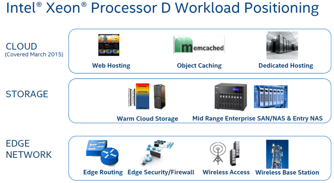
Xeon D was launched with two SKUs (D1520, a 4C/8T SiP, and the D1540, a 8C/16T SiP) earlier this year. While those two SKUs covered the web hosting applications, today's launches cover the storage and edge network applications. Intel's slide from a presentation made earlier today sums up the various products in the lineup. Eight new Xeons and three new Pentium processors are being launched in the D-1500 lineup and they come in both 45W and 35W TDP versions. Interestingly, Intel indicated that 12-core and 16-core Xeon D SiPs can be expected early next year.
Patrick at ServeTheHome has a nice graphic summarizing the clock speeds and pricing of these products. The D15x1 SKUs target the storage market, while the D15x7 and D15x8 target the networking / communication segments.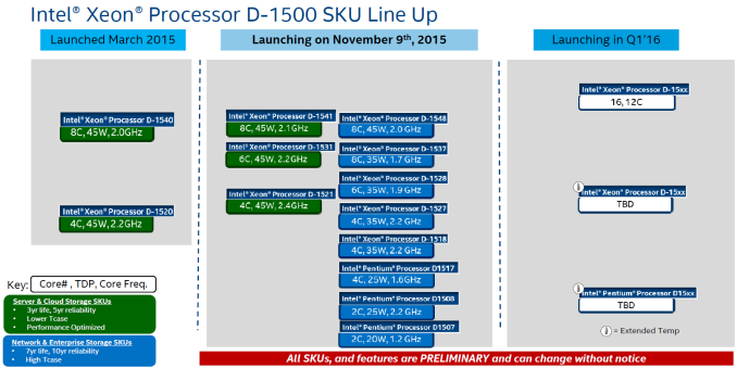
Intel claims that the new storage SKUs provide as much as 6x the performance of the high-end Avoton-based platforms.
Intel's Storage Acceleration Library (ISA-L) provides accelerators for compression, checksumming, parity calculation and cryptograhic functions (encryption as well as hashing).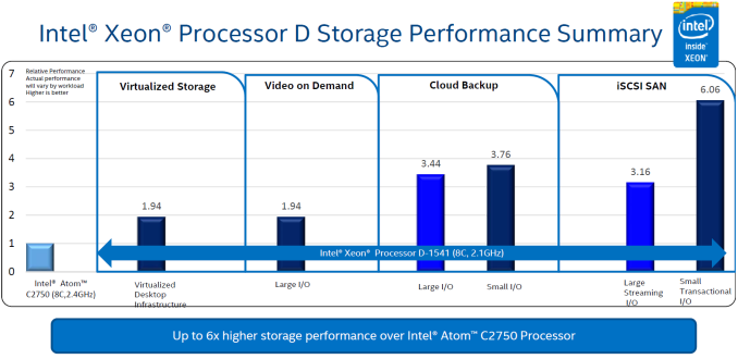
The Storage Performance Development Kit (SPDK) provides better optimization compared to the native Linux drivers - particularly as the number of storage devices in the system ramps up.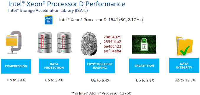
On the networking front, Intel claims up to 5.4x higher performance compared to the Rangeley-based platforms. Intel is promoting their Data Plane Development Kit (DPDK) to achieve better performance for L3 packet forwarding, VM packet forwarding with Open vSwitch, and IPSec forwarding (VPN applications).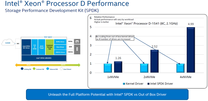
ServeTheHome talks about how the communication accelerators have gained extensive software support since they were launched with the Rangeley SoCs in 2013.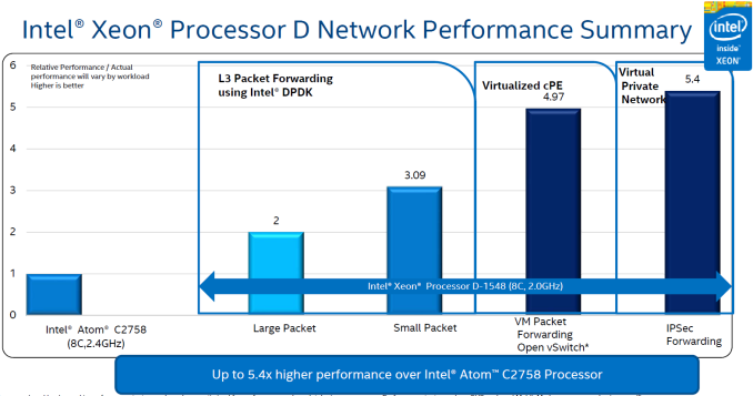
One of the disappointing aspects with respect to the D1520 and D1540 (at least for those intending to use them as virtualization hosts) was the pulling back of the advertised SR-IOV feature. It remains to be seen if the new SKUs have the feature enabled.
In addition to the new Xeon D SKUs, Intel also announced the FM10000 Ethernet multi-host controller family that can provide up to 36 Ethernet lanes. The FM10000 family supports 1Gbps, 2.5Gbps, 10Gbps, and 25Gbps Ethernet ports and the ability to group four lanes as 40Gbps or 100Gbps ports. The integrated Ethernet controllers can be configured as four 50Gbps or eight 25Gbps host interfaces,.
The new X550 single-chip, low-cost 10GbE platform was also launched. It supports NBASE-T technology (for 2.5Gbps as well as 5 Gbps operation, in addition to 10Gbps).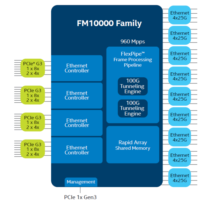
Operating via a PCIe 3.0 x1 / x4 / x8 link, the new 10GBASE-T controller integrates both MAC and PHY in a single package, and comes in both single and dual-port varieties. Power consumption is just 11 W with both 10GbE ports active, making it amenable to passive heatsink thermal solutions.
More...
-
11-10-15, 04:20 AM #5476
Anandtech: Imagination Announces New P6600, M6200, M6250 Warrior CPUs
Today Imagination launches three new MIPS processor IPs: One in the performance category of Warrior CPUs, the P6600 and two embedded M-class core, the M6200 and M6250.
Warrior P6600
Starting off with the P6600, this is Imagination's new MIPS flagship core succeeding the P5600. The P5600 was a 3-wide out-of-order design with a pipeline depth of up to 16 stages. The P6600 keeps most of the predecessor's characteristics such as hardware multi-threading of up to 4 threads per core, full hardware virtualization and security through OmniShield, but adds compatibility for MIPS64 64-bit processing on top. Imagination first introduced a mobile oritented 64-bit MIPS CPU back with the I6400 a little more than a year ago but we've yet to see vendors announce products with it.
We're still lacking any details on the architectural improvements of the P6600 over the P5600 so it seems that for now we're left with guessing what kind of performance the new core will bring. The P5600 was directly competing with ARM's Cortex A15 in terms of IPC, but ARM has since then not only announced but also seen silicon with two successor IPs to the A15 (A57 and A72), so the P6600 will have some tough competition ahead of itself once it arrives in products.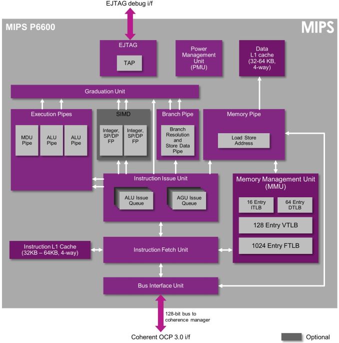
The P6600, much like the P5600 can be implemented from single-core to six-core cluster configurations. What is interesting that as opposed to ARM CPU IP, the MIPS cores allow for asynchronous clock planes between the individual cores if the vendors wishes to implement the SoC's power management in this way (It can also be set up to work in a synchronous way).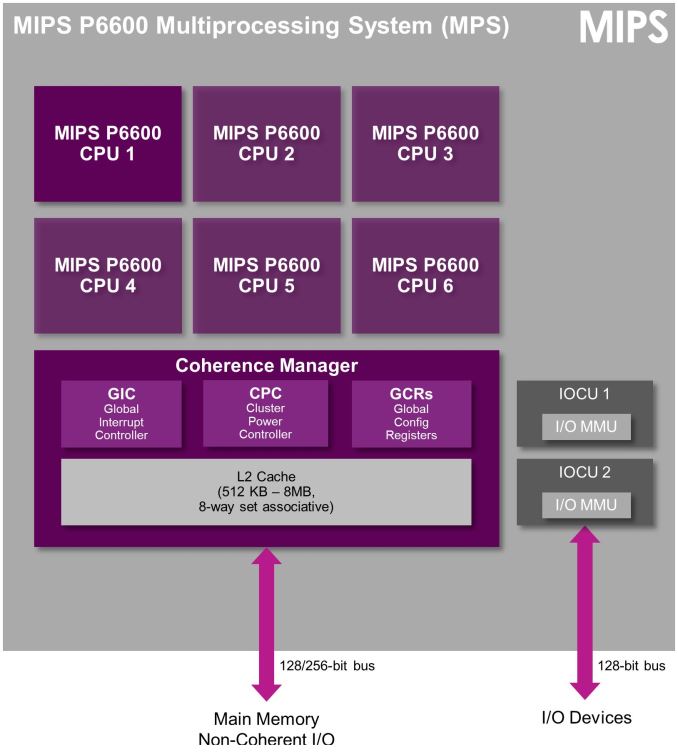
"MIPS P6600 is the next evolution of the high-end MIPS P-class family and builds on the 32-bit P5600 CPU. P6600 is a balanced CPU for mainstream/high-performance computing, enabling powerful multicore 64-bit SoCs with optimal area efficiency for applications in segments including mobile, home entertainment, networking, automotive, HPC or servers, and more. Customers have already licensed the P6600 for applications including high-performance computing and advanced image and vision systems."Warrior M6200 & M6250
Also as part of today's announcement we see two new embedded CPU cores, the M6200 and M6250. Both cores are successors to the microAptiv-UP and UC but able to run at up to 30% higher frequency. The new processors also see an ISA upgrade to MIPS32 Release 6 instead of Release 5.
The M6200 is targeted at real-time embedded operating systems with minimal funtionality for cost- and power-savings. It has no MMU and as such can only be described as a microcontroller part.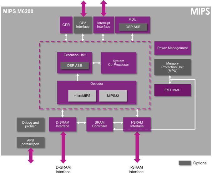
The M6250 is the bigger brother of the M6200 and the biggest difference is the inclusion of a memory management unit (MMU) that makes this a full fledged processor core that can run operating systems like Linux.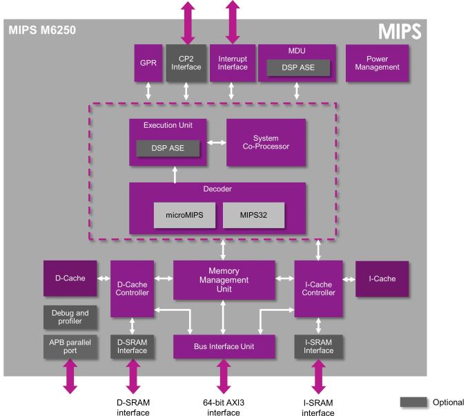
"M6200 and M6250 are configurable and fully synthesizable solutions for devices requiring a high level of performance efficiency and small silicon area including wireless or wired modems, GPU supervisors, flash and SSD controllers, industrial and motor control, advanced audio and more."
More...
-
11-10-15, 07:07 AM #5477
Anandtech: The Microsoft Surface Book Review
Microsoft has released what they are calling "The Ultimate Laptop" and with their first attempt at moving outside the tablet segment, we take a look at the new Surface Book and how it compares. Competition in the notebook segment is much more intense than the high end tablet market, and Microsoft is aiming for the top.
More...
-
11-10-15, 08:14 AM #5478
Anandtech: NVIDIA Announces Tesla M40 & M4 Server Cards - Data Center Machine Learnin
Slowly but steadily NVIDIA has been rotating in Maxwell GPUs into the company’s lineup of Tesla server cards. Though Maxwell is not well-suited towards the kind of high precision HPC work that the Tesla lineup was originally crafted for, Maxwell is plenty suitable for just about every other server use NVIDIA can think of. And as a result the company has been launching what’s best described as new breeds of Maxwell cards in the last few months.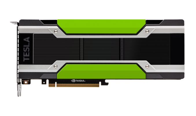
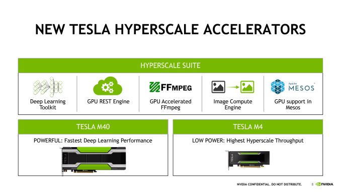
After August’s announcement of the Tesla M60 and M6 cards – with a focus on VDI and video encoding – NVIDIA is back today for the announcement of the next set of Tesla cards, the M40 and the M4. In what the company is dubbing their “hyperscale accelerators,” NVIDIA is launching these two cards with a focus on capturing a larger portion of the machine learning market.
 First let’s quickly talk about the cards themselves. The Tesla M40 marks the introduction of the GM200 GPU to the Tesla lineup, with NVIDIA looking to put their best single precision (FP32) GPU to good use. This is a 250 Watt full power and fully enabled GM200 card – though with Maxwell this distinction loses some meaning – with NVIDIA outfitting the card with 12GB of GDDR5 VRAM clocked at 6GHz. We know that Maxwell doesn’t support on-chip ECC for the RAM and caches, but it’s not clear at this time whether soft-ECC is supported for the VRAM. Otherwise, with the exception of the change in coolers this card is a spitting image of the consumer GeForce GTX Titan X.
NVIDIA Tesla Family Specification Comparison Tesla M40 Tesla M4 Tesla M60 Tesla K40 Stream Processors 3072 1024 2 x 2048
(4096)2880 Boost Clock(s) ~1140MHz ~1075MHz ~1180MHz 810MHz, 875MHz Memory Clock 6GHz GDDR5 5.5GHz GDDR5 5GHz GDDR5 6GHz GDDR5 Memory Bus Width 384-bit 128-bit 2 x 256-bit 384-bit VRAM 12GB 4GB 2 x 8GB
(16GB)12GB Single Precision (FP32) 7 TFLOPS 2.2 TFLOPS 9.7 TFLOPS 4.29 TFLOPS Double Precision (FP64) 0.21 TFLOPS (1/32) 0.07 TFLOPS (1/32) 0.3 TFLOPS (1/32) 1.43 TFLOPS (1/3) Transistor Count 8B 2.94B 2x 5.2B 7.1B TDP 250W 50W-75W 225W-300W 235W Cooling Passive Passive
(Low Profile)Active/Passive Active/Passive Manufacturing Process TSMC 28nm TSMC 28nm TSMC 28nm TSMC 28nm GPU GM200 GM206 GM204 GK110 Target Market Machine Learning Machine Learning VDI Compute
Joining the Tesla M40 is the Tesla M4. As hinted at by its single-digit product number, the M4 is a small, low powered card. In fact this is the first Tesla card to be released in a PCIe half-height low profile form factor, with NVIDIA specifically aiming for dense clusters of these cards. Tesla M4 is based on GM206 – this being the GPU’s first use in a Tesla product as well – and is paired with 4GB of GDDR5 clocked at 5GHz. NVIDIA offers multiple power/performance configurations of the M4 depending on server owner’s needs, ranging from 50W to 75W, with the highest power mode rated to deliver up to 2.2TFLOPS of FP32 performance.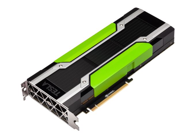
Both the Tesla M40 and M4 are being pitched at the machine learning market, which has been a strong focus for NVIDIA since the very start of the year. The company believes that machine learning is the next great frontier for GPUs, capitalizing on neural net research that has shown GPUs to be capable of both quickly training and quickly executing neural nets. Neural nets in turn are increasingly being used as more efficient means for companies to process vast amounts of audio & video data (e.g. the Facebooks of the world).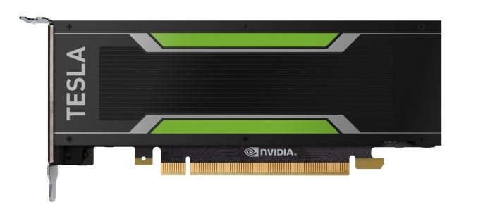
To that end we have seen the company focus on machine learning in the automotive sector with products such as the Drive PX system and lay out their long-term plans for machine learning with the forthcoming Pascal architecture at GTC 2015. In the interim then we have the Tesla M40 and Tesla M4 for building machine learning setups with NVIDIA’s current-generation architecture.
Given their performance and power profiles, Tesla M40 and M4 are intended to split the machine learning market on the basis of training versus execution The powerful M40 being well-suited for quicker training of neural nets and other systems, while the more compact M4 is well-suited for dense clusters of systems actually executing various machine learning tasks. Note that it’s interesting that NVIDIA is pitching the M40 and not the more powerful M60 for training tasks; as NVIDIA briefly discussed among their long-term plans at GTC 2015, current training algorithms don’t scale very well beyond a couple of GPUs, so users are better off with a couple top-tier GM200 GPUs than a larger array of densely packed GM204 GPUs. As a result the M40 occupies an interesting position as the company’s top Tesla card for machine learning tasks that aren’t trivially scalable to many GPUs.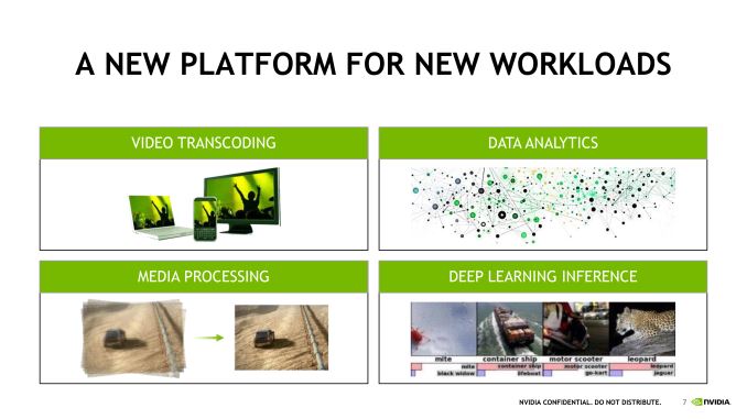
Meanwhile, along with today’s hardware announcement NVIDIA is also announcing a new software suite to tie together their hyperscale ambitions. Dubbed the “NVIDIA Hyperscale Suite,” the company is putting together software targeted at end-user facing web services. Arguably the lynchpin of the suite is NVIDIA’s GPU REST Engine, a service for RESTful APIs to utilize the GPU, and in turn allowing web services to easily access GPU resources. NVIDIA anticipates the GPU REST Engine enabling everything from search acceleration to image classification, and to start things off they are providing the NVIDIA Image Compute Engine, a REST-capable service for GPU image resizing. Meanwhile the company is also be providing their cuDNN neural net software as part of the suite, and versions of FFmpeg with support for NVIDIA’s hardware video encode and decode blocks to speed up video processing and transcoding.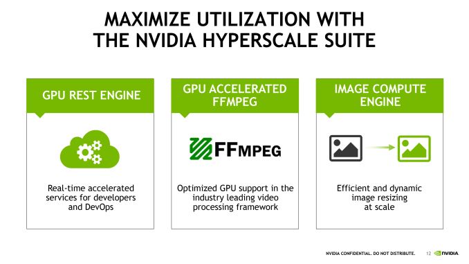
Wrapping things up, as is common with Tesla product releases, today’s announcements will predate the hardware itself by a bit. NVIDIA tells us that the Tesla M40 and the hyperscale software suite will be available later this year (with just over a month and a half remaining). Meanwhile the Tesla M4 will be released in Q1 of 2016. NVIDIA has not announced card pricing at this time.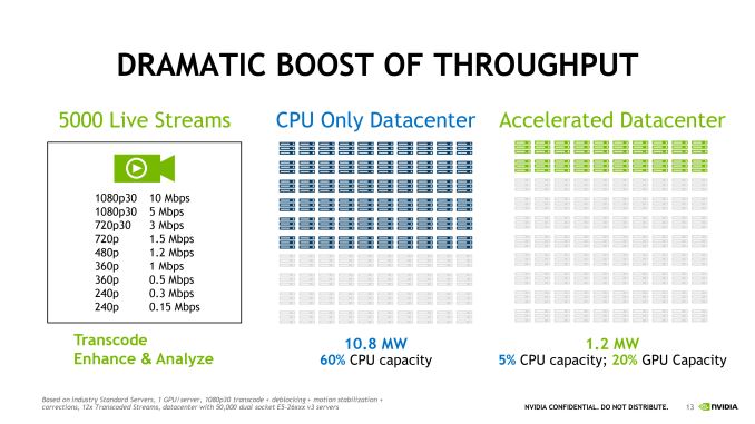
Gallery: Tesla M40, Tesla M4, & Hyperscale Software Suite Announcement


More...
-
11-10-15, 10:35 AM #5479
Anandtech: Google Begins Offline Maps Rollout on Android
Earlier this year at Google I/O it was announced that Google Maps for Android and iOS would be receiving an update that would add the ability to save maps for online viewing. Interestingly enough, this feature has actually existed and been removed from Google Maps on more than one occasion, and so such a prominent announcement gave some hope that it would stick around for good this time. Today the update is finally rolling out to Maps users on Android.
The feature works in a fairly straightforward manner. When searching a location in maps there will now be a download button in the information page about that location. You can then scroll around to fit the parts of the map you need into the box shown on screen, and when you name and save it the maps for that area will be permanently stored on your device. The applications for this feature are fairly obvious, such as storing maps of areas where you won't have a cell signal, or of places you'll be travelling to in other countries where your phone won't work.
The new version of Google Maps with offline maps is rolling out now on Android, and an updated version for iOS will be coming in the near future.
More...
-
11-10-15, 12:30 PM #5480
Anandtech: ARM Announces New Cortex-A35 CPU - Ultra-High Efficiency For Wearables & M
Today as part of the volley of announcements at ARM's TechCon conference we discover ARM's new low-power application-tier CPU architecture, the Cortex-A35. ARM follows an interesting product model: The company chooses to segment its IP offerings into different use-cases depending on market needs, designing different highly optimized architectures depending on the target performance and power requirements. As such, we see the Cortex-A lineup of application processors categorized in three groups: High performance, high efficiency, and ultra-high efficiency designs. In the first group we of course find ARM's big cores such as the Cortex A57 or A72, followed by the A53 in more efficiency targeted use-cases or in tandem with big cores in big.LITTLE designs.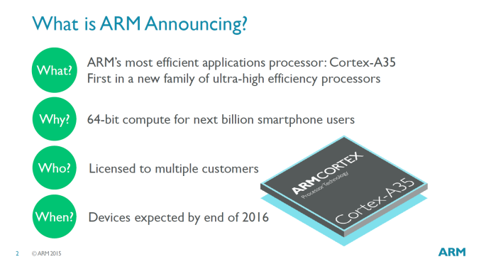
What seems to be counter-intuitive is that ARM sees the A35 not as a successor to the A53, but rather a replacement for the A7 and A5. During our in-depth analysis of the Cortex A53 in our Exynos 5433 review earlier this year I claimed that the A53 seemed to be more like an extension to the perf/W curve of the Cortex A7 instead of it being a part within the same power levels, and now with the A35 ARM seems to have validated this notion.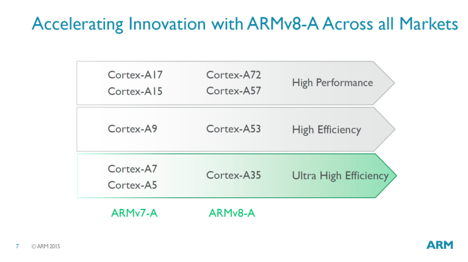
As such, the A35 is targeted at power targets below ~125mW where the Cortex A7 and A5 are still very commonly used. To give us an idea of what to expect from actual silicon, ARM shared with us a figure of 90mW at 1GHz on a 28nm manufacturing process. Of course the A35 will see a wide range of implementations on different process nodes such as for example 14/16nm or at much higher clock rates above 2GHz, similar to how we've come to see a wide range of process and frequency targets for the A53 today.
Most importantly, the A35 now completes ARM's ARMv8 processor portfolio with designs covering the full range of power and efficiency targets. The A35 can also be used in conjunction with A72/A57/A53 cores in big.LITTLE systems, enabling for some very exotic configurations (A true tri-cluster comes to mind) depending if vendors see justification in implementing such SoCs.
At heart, the A35 is still an in-order limited dual-issue architecture much like the A7 or A53. The 8-stage pipeline depth also hasn't changed so from this high-level perspective we don't see much difference in comparison to preceding designs. What ARM has done though is to improve the individual blocks for better performance and efficiency by having bits and pieces of architectural enhancements that are even newer than what big cores such as the A72 currently employ.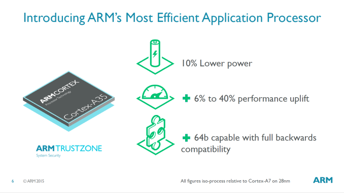
Areas where the A35 had focused attention on are front-end efficiency improvements, such as a redesigned instruction fetch unit that improves branch prediction. The instruction fetch bandwidth was balanced for power efficiency while the instruction queue is now smaller and also tuned for efficiency.
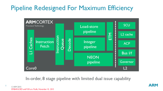
It's especially on memory benchmarks where the A35 will shine compared to the A7: The A35 adopts a lot of the Cortex A53's memory architecture. On the L1 memory system of which A35 can have configurable 8 to 64KB of instruction and data caches we now see use of multi-stream automatic data prefetching and automatic write stream detection. The L2 memory system (configurable from 128KB to 1MB) has seen increased buffering capacity and resource sharing while improving write stream efficiency and introducting coherency optimizations to reduce contention.
The NEON/FP pipeline has seen the biggest advancements, besides improved store performance the new units now add fully pipelined double precision multiply capability. The pipeline has also seen improvements in terms of area efficiency, part of the reason enabling the A35 to be smaller than the A53.
In terms of power management, the A35 much like the A53 now implements hardware retention states for both the main CPU core and NEON pipeline (separate power domains). What seems to be interesting here is that there is now a hardware governor within the CPU cluster able to arbitrate automatic entry and exit for retention states. Until now we've seen very little to no use of retention states by vendors, the only SoC that I've confirmed to use it was the Snapdragon 810 and that was subsequently disabled in later software updates in favour of just using the core power collapse CPU idle state.
At the same frequency and process, the A35 architecture (codenamed Mercury), promises to be 10% lower power than the A7 while giving an 6-40% performance uplift depending on use-case. In integer workloads (SPECint2006) the A35 gives about 6% higher throughput than the A7, while floating point (SPECfp2000) is supposed to give a more substantial 36% increase.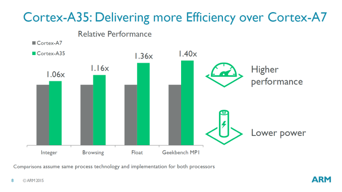
What is probably more interesting are apples-to-apples performance and power comparisons to the A53. Here the A35 actually is extremely intriguing as it is able to match the A53's performance from 80% to up to 100% depending on use-case. Browser workloads are where the A35 will trail behind the most and only be able to provide around 80% of the A53's performance. Integer workloads are quoted at coming in at 84-85% of the Apollo core, while as mentioned earlier, memory-heavy workloads at supposed to be on par with the larger bretheren.
What puts things in perspective though is that the A35 is able to achieve all of this at 75% the core size and 68% the power of the A53. ARM claims that the A35 and A53 may still be used side-by-side and even envisions big.LITTLE A53.A35 designs, but I have a hard time justifying continued usage of the A53 because of the cost incentive for vendors to migrate over to the A35. Even in big.LITTLE with A72 big cores I find it somewhat hard to see why a vendor would choose to continue to use an A53 little cluster while they could theoretically just use a higher clocked A35 to compensate for the performance deficit. Even in the worst-case scenario where the power advantage would be eliminated by running a higher frequency, vendors would still be able to gain from the switch due to the smaller core and subsequent reduced die size.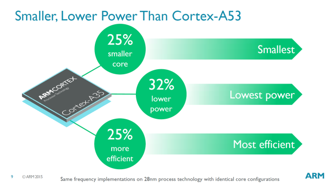
The A35 is touted as ARM's most configurable processor with vendors able to alter their designs far beyond simple choices such the core-count within a cluster. Designers will now also be able to choose whether they want NEON, Crypto, ACP or even the L2 blocks included in their implementations. The company envisions this to be processor for the next billion smartphone users and we'll likely see it in a very large variety of SoCs powering IoT devices such as wearables and embedded platforms, to budget smartphones and even high-end ones in big.LITTLE configurations.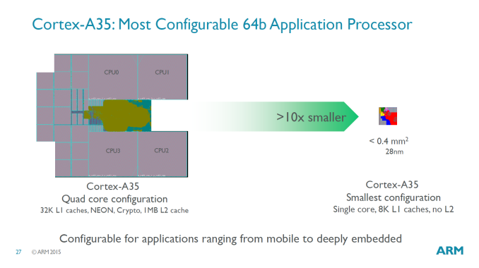
ARM expects first devices with the A35 to ship by the end of 2016. Due to the sheer number of possible applications and expected volume, the Cortex A35 will undoubtedly be a very important CPU core for ARM that will be with us for quite some time to come.
More...


 Quote
QuoteThread Information
Users Browsing this Thread
There are currently 8 users browsing this thread. (0 members and 8 guests)


Bookmarks