

Results 5,811 to 5,820 of 12096
Thread: Anandtech News
-
03-10-16, 02:30 PM #5811
Anandtech: EUV Lithography Makes Good Progress, Still Not Ready for Prime Time
At the recent annual SPIE Advanced Lithography conference, Intel, TSMC and other leading semiconductor companies said that significant strides have been made in extreme ultraviolet lithography (EUVL) over the past year or so. Intel did not reveal when exactly it plans to start using EUV technology, but indicated that it will clearly utilize it once it is suitable for high-volume production of semiconductors and is enough cost effective. Samsung and TSMC also intend to start inserting EUVL tools into production in the coming years.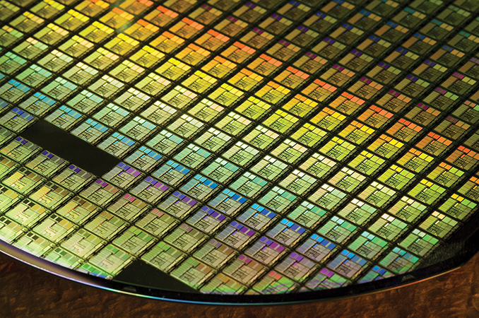
Chip Production Gets Harder
As chipmakers transit to newer process technologies every several years, sizes of transistors and electronic circuits within microprocessors shrink, making them more complex and powerful, but also harder to manufacture using traditional photolithographic methods. Feature sizes of today’s circuits within modern chips can be as small as 42 nm, whereas modern semiconductor production tools use deep ultraviolet (DUV) argon fluoride (ArF) excimer lasers with 193 nm wavelength. To compensate for this difference, Intel and other makers of advanced chips use multiple techniques to enhance resolution of photolithographic equipment.
One of the key transistor density improving technologies is immersion lithography, which replaces the air gap between the lens and wafer with liquid, whose refraction index is higher than one. For example, purified deionized water has refraction index of 1.44 and this allows to enhance resolution of production tools by up to 40% depending on materials. Another key tech for contemporary semiconductor manufacturing is called multiple patterning, a semiconductor production technique that allows to increase feature density by resolving multiple lines on the same photoresist layer using multiple photomasks. Usage of multi-patterning essentially means that certain layers within one chip are exposed multiple times, which greatly increases complexity of manufacturing operations and stretches production cycles, essentially increasing costs of chips.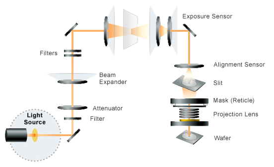
Intel has been using multi-patterning since mid-2000s and its 65 nm manufacturing technology. The technique did not cause a lot of troubles at first, but things got very complicated with the 14 nm fabrication process because the number of mask steps significantly increased compared to previous-gen technologies. Meanwhile it is taking the company longer to develop its 10 nm manufacturing process, tune its designs and achieve high yields than it used to be, which is why the company had to delay its Cannonlake CPUs from 2016 to 2017. It's also important to note that Intel's 14nm process introduced air gap dielectric in certain interconnect layers, which dramatically increased the number of engineering problems to overcome as introducing voids into the interconnect leads to structural instabilities that must be controlled appropriately.
Basically, as it becomes increasingly tougher to develop new manufacturing technologies and produce modern chips using currently available tools, the benefits of node-to-node transitions shrinks, which is rather dangerous for chipmakers from an economic standpoint. In order to address negative effects of multi-patterning, producers of step and scan systems used in semiconductor manufacturing significantly increased output of such tools, as well as enhanced their resolution and boosted their overlay and focus performance. For example, ASM Lithography (ASML), the world’s largest maker of scanners, claims that its latest TWINSCAN NXT:1980Di can process up to 275 wafers per hour and can be used to make chips using sub-10 nm process technologies. While such scanners will be utilized going forward, with so many mask steps required, a new method of photolithography will make far more sense.
EUV Makes a Big Promise, But Generates Big Challenges
EUV lithography, whose development started in 1985 and which used to be called Soft X-Ray, utilizes extreme ultraviolet wavelength of 13.5 nm. Using EUV can greatly enhance the feature density of chips without heavy reliance on multi-patterning and additional layers. For example, TSMC can produce 46 nm metal pitches with a single exposure, an operation that requires usage of four masks for an ArF scanner. Moreover, Intel has managed to produce wafers with 22 nm metal pitches using its own micro EUV tool. Among other advantages, EUV is expected to shrink cycle times and promises to increase yields of chips at advanced nodes. Unfortunately, EUV is an extremely complex technology that not only requires all-new step-and-scan systems for production of semiconductors, new chemicals and new mask infrastructure, but it is also so tricky to use that its actual resolution can end up far below expectations.
It should be noted that generation of EUV light is a rather difficult process itself. Cymer, a division of ASML that produces light sources for lithography tools, is developing laser produced plasma (LPP) EUV sources. The LPP technology applies CO2 laser to small tin droplets (which are around 30 microns in diameter), creating ionized gas plasma at electron temperatures of several tens of electron volts. The 13.5 nm radiation is then collected by a special ~0.5 meter mirror coated with several layers of molybdenum (Mo) and silicon (Si), in order to selectively reflect the maximum possible amount of 13.5 nm EUV light and direct it to the Intermediate Focus (IF) position at the entrance to the scanner system.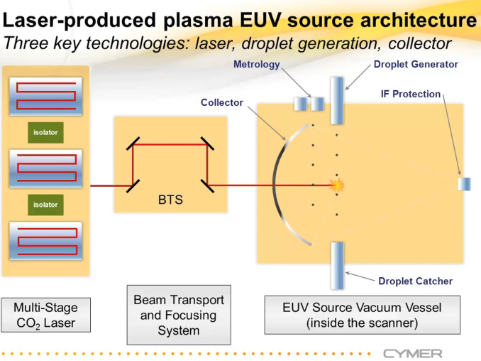
To put it simply: in order to generate 13.5 nm EUV light in a special plasma chamber, you need a very powerful laser (because a significant amount of its power will be wasted); a generator and a catcher for tin droplets (in addition to a debris collector); as well as a special, nearly perfect, elliptical mirror. To make everything even trickier, since EUV light with 13.5 nm wavelength can be absorbed by almost any matter, EUV lithography has to be done in vacuum. This also means that traditional lenses cannot be used with EUV because they absorb 13.5 nm light; instead, specialized multilayer mirrors are used. Even such mirrors absorb about 30% of the light, which is why powerful light sources are needed. This level of absorption can lead to ablative effects on the mirrors themselves, which introduces additional engineering challenges. To learn more how EUV LPP light sources work, check out this video.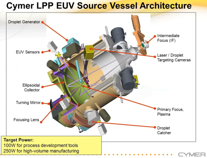
The 13.5 nm EUV light generator needs to have a powerful light source that can expose economically viable amount of wafers per hour (or day). One of the key issues with the TWINCSCAN NXE scanners was that is their laser produced plasma EUV source was not powerful enough. Until recently, performance of experimental EUV equipment from ASML, such as the TWINCSCAN NXE:3300B scanners, was limited to around 500 wafers per day due to power source limitations. By contrast, the current-generation TWINSCAN NXT scanners can process from 175 to 275 wafers per hour (which is good enough, considering heavy usage of multi-patterning). The reliability of the droplet generator was mediocre just about a year ago. Moreover, lifetime of the collector mirror is a yet another point of concern due to the previously mentioned ablative effects.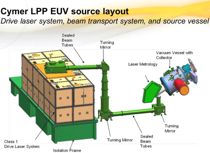
Things Are Getting Better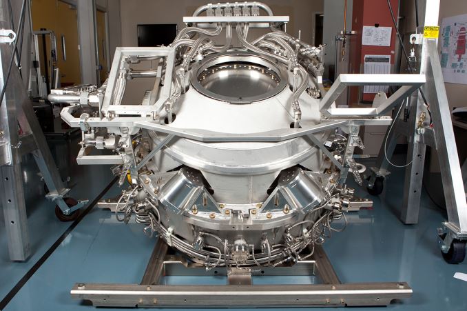
The progress of EUVL scanners as well as EUV source systems has been steady in the recent years. ASML, which is one of the major driving forces for extreme ultraviolet lithography, recently said it had hit multiple stability, availability and productivity targets in 2014 and 2015 and is optimistic about the future.
According to ASML, in 2015 one of the company’s clients managed to expose more than 1000 wafers per day on the NXE:3300B, whereas ASML itself managed to hit 1250 wafers per day milestone on the NXE:3350B. ASML also said that it could operate a 200 W light source for one hour with full dose control. For HMV (high volume manufacturing) equipment, 250 W light sources will be needed. ASML is not sure when such light source will be made, but it hopes to hit this milestone in 2016 or 2017. Hence, there is still a long way to go for suitably powerful EUV light sources.
At the SPIE Advanced Lithography conference, Intel confirmed that there were four running EUV tools with 80 W light sources around the world as of early 2016, up from one a year ago. Intel itself now uses the NXE:3300B tool with Cymer’s 80 W EUV sources on its 14 nm pilot line for 21 hours per day, leaving three hours for engineering and servicing. Britt Turkot, senior principal engineer in logic technology development lithography at Intel, said that experimental EUV production had demonstrated good overlay trends, stable critical dimension uniformity as well as good electrical testing and end-of-line yield results.
Another piece of good news is that the reliability of the tin droplet generator also improved significantly over the past year. Intel indicated that the tin droplet generator now achieves 85% of its expected lifetime. Reflectivity of the elliptical collector also degrades in accordance with expectations. ASML and Intel are also seeing combined scanner and source availability (4-week rolling average) exceeding 70%, which is good enough for development, but is still unacceptable for mass production. ASML plans to increase availability of its tools to 80% this year.
EUV Photomask Industry Needs Further Development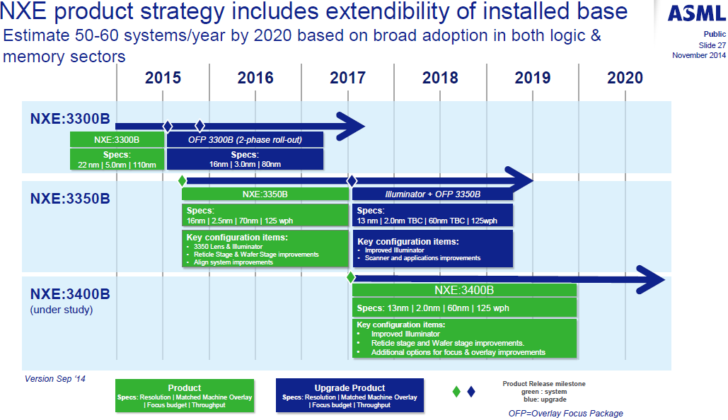
Extreme ultraviolet lithography no longer uses lenses and traditional glass photomasks (reticles), but utilizes specialized mirrors as well as multi-layer reflective photomasks. Even a minor defect in a photomask makes it unusable because it affects the final wafer. To discover such defects, makers of photomasks or chips can use currently available optical mask inspection tools, e-beam/multi e-beam tools (which are slow) or actinic patterned mask inspection tools, the latter of which have not been commercialized yet. For now, optical mask inspection tools based on 193 nm or other wavelengths can be used for EUV photomasks, but there is a problem.
Since photomasks (reticles) in extreme ultraviolet lithography are even more vulnerable than conventional glass photomasks, they can be easily damaged by falling particles during exposure or even by 13.5 nm EUV light itself. To address this issue, Intel and ASML have been working collaboratively to add a special pellicle to protect the photomask. Protective films for EUV should be extremely thin, should not affect reflection characteristics of photomasks, and should sustain EUV power levels. Unfortunately, it is impossible to use currently available 193 nm mask inspection tools like scanning or tunneling electron microscopes to review an EUV reticle with a pellicle on it, according to SemiEngineering and industry sources. Only actinic patterned mask inspection (APMI) tools are useful for this purpose. However, the latter are not available today outside of academic labs like Berkeley's SHARP mask imaging microscope. As a result, semiconductor companies had to invent a way for mask shops to inspect reticles without pellicles using contemporary equipment and then install protection before shipping masks to fabs (which means that it will be impossible to inspect photomasks after the fact at fabs using current tools). According to the world’s largest CPU maker, its pelliclized reticles can sustain over 200 wafer exposures. However, defectivity levels on such pellicle membranes are still high, which means that flaws can essentially affect wafers and dramatically lower yields. Moreover, it remains to be seen whether producers can supply enough of such membranes.
What is even more important is that to inspect reflective photomasks for EUVL, chipmakers will still need actinic patterned mask inspection equipment. Without such tools and timely repair of photomasks using e-beam tools, yields will inevitably become an issue, Intel has said. Since APMI tools do not exist today (even though KLA-Tencor is said to be developing such devices), it will take years before they reach the market. Moreover, such equipment will not be cheap, they will resemble scanners and will require EUV light sources.
At the SPIE conference, Intel demonstrated successful defect mitigation strategies on multiple devices, and a healthy e-beam pattern defect repair capability. So, the situation with mask inspection and repairs is improving, according to the CPU maker.
EUV Is Required for 7 nm Technology, But Will Be Implemented “When It’s Done”
In general, the industry remains rather optimistic about EUV lithography thanks to two years of solid progress. All leading makers of semiconductors, including Intel, TSMC, Samsung and GlobalFoundries plan to use EUV tools as soon as it makes sense. All four chipmakers indicated on various occasions in the recent months that EUV lithography will be required for 7 nm manufacturing technology. At the SPIE conference, TSMC and Samsung re-affirmed plans to insert EUVL into 7 nm production. By contrast, Intel indicated that while it would prefer to use EUVL for critical layers at 7 nm, it would only use the tech when it is completely ready. At present, Intel is experimenting with EUV on its 14 nm pilot fab line and the results have been encouraging, according to the company. Nonetheless, Intel believes that to make EUV a reality, in addition to many other things, the industry needs to improve yields, decrease costs and develop an ecosystem of EUV photomasks.
Finally, while step-and-scan systems with EUV's 13.5 nm wavelength will help to produce microprocessors and other chips using 5 nm and, perhaps, 7nm, technologies, contemporary 193nm ArF tools are not going anywhere. Virtually all chipmakers say that EUV scanners will only be used for critical layers of chips. For layers that can be produced using multi-patterning, DUV tools will be used.
Intel, TSMC and Samsung have publicly said that they plan to start producing chips using their 10 nm manufacturing technologies in 2017. These process technologies have already been developed without EUV, and unless the chipmakers decide to introduce new versions that involve EUV for critical layers, EUV will continue to not be used for 10 nm. The leading makers of semiconductors are currently finalizing their 7 nm technologies this year, and they will have to make decisions regarding usage of EUV tools with their 7 nm nodes in 2018 – 2019, according to Peter Wennink, CEO of ASML. If currently available EUV tools meet expectations of chipmakers, they will order production TWINSCAN NXE systems and will use them two or three years down the road.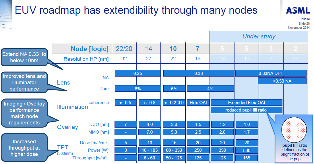
Sources: Intel, Semiconductor Engineering, Semiconductor Manufacturing and Design, SemiWiki.
Images courtesy of ASML, Cymer, TSMC.
More...
-
03-11-16, 07:19 AM #5812
Anandtech: The Intel NUC6i5SYK Skylake UCFF PC Review
The evolution of computing platforms has left the traditional desktop PC market in a precarious state. However, the miniaturization trend has provided some bright spots. Compact PCs have been around in the mini-ITX form factor for a relatively long time now. The market segment received a massive boost with the introduction of the ultra-compact form factor (UCFF) machines. It all started with the first Intel NUC (Next Unit of Computing) based on a Sandy Bridge processor. Every generation since Sandy Bridge has seen multiple NUCs based on the corresponding U-series processors, and Skylake is no different. Read on for our review of the Intel NUC6i5SYK based on the Intel Core i5-6260U.
More...
-
03-11-16, 08:32 AM #5813
Anandtech: ZOTAC to Offer Small Form-Factor PC with NVIDIAs GeForce GTX 980 GPU
Various kinds of small form-factor PCs are on a roll these days. Mini-ITX systems have been offering performance of full-size desktops for several years now and even smaller systems are catching up in terms of performance. ZOTAC this week said that it had developed an SFF PC with NVIDIA’s mobile GeForce GTX 980 inside. The new system will be showcased at CeBIT and GDC trade-shows this month and will be available later in 2016.
The ZOTAC ZBOX MAGNUS EN980 is based on an unnamed Intel Core i-series processor based on the Skylake micro-architecture as well as NVIDIA’s mobile GeForce GTX 980 graphics adapter. The card boasts with a fully-fledged GM204 GPU with 2048 stream processors, 128 texture units, 64 raster operations pipelines as well as a 256-bit memory interface. Performance of the mobile GeForce GTX 980 (which is not a card, but an MXM module) is similar to that of a desktop graphics board with the same brand name. It is unknown whether the version of the mobile GTX 980 is equipped with 4 GB or 8 GB of GDDR5 memory.
The TDP of the mobile GeForce GTX 980 is 145 W, which is lower compared to a desktop GeForce GTX 980 (which dissipates up to 165 W), but is still very high. In a bid to cool-down the system with a 145 W GPU inside, ZOTAC had to invent a new liquid-cooling solution with multiple liquid channels and heat pipes. The company does not say a lot about its cooler right now and also does not show the final design of the PC. The only thing that ZOTAC officially demonstrated so far is the picture of the top cover of the system. Based on design pattern (which looks like comb, a pattern that is known to be efficient in dissipation of heat), it seems that heat dissipation was among ZOTAC’s primary concerns about this system. Another thing to worry about was acoustics: it is not easy to cool-down an SFF PC that dissipates over 160 W of power (even in case ZOTAC sticks to an ULV CPU, it will still have TDP of at least 15 W) without using high-speed/high-pressure fans. According to the company, it has managed to solve the problem thanks to its liquid cooling system and the PC is “whisper quiet”. The upcoming ZBOX MAGNUS EN980 packs a lot of processing horsepower and uses sophisticated cooling, but not at the cost of elegant appearance. The overall design of the ZBOX MAGNUS EN980 should look rather stylish thanks to grey metal with aquamarine inlays.
ZOTAC yet has to announce all the details about its ZBOX MAGNUS EN980. At present, the company only says that apart from an Intel Skylake CPU and the GeForce GTX 980 GPU, the system features two Gigabit Ethernet controllers, one IEEE 802.11ac Wi-Fi and Bluetooth wireless module, a USB 3.1 controller with at least one type-C connector and so on. Keeping in mind rather advanced expansion capabilities of the ZBOX MAGNUS EN970, expect the new system to feature an M.2 SSD, one or two 2.5” HDD, multiple HDMI 2.0 outputs, an SD card reader and so on.
ZOTAC positions its new ZBOX MAGNUS as a small form-factor PC for VR gaming. The minimum graphics cards recommended for virtual reality by Oculus VR is AMD Radeon R9 290 or NVIDIA GeForce GTX 970. The MAGNUS EN980 can beat both of those graphics cards, so, there will be even a slight performance headroom in terms of graphics processing horsepower. What remains to be seen is which processor ZOTAC plans to use for its premium SFF desktop. Oculus VR recommends quad-core Intel Core i5-4590 (3.30 – 3.70 GHz, 6 MB cache) microprocessor (or equivalent) for VR Ready systems. Therefore, if ZOTAC wants to meet the guidelines, it will have to install a rather powerful quad-core CPU into its MAGNUS EN980.
The ZOTAC ZBOX MAGNUS EN980 will be demonstrated at CeBIT and GDC trade-shows in the coming weeks. The manufacturer does not reveal anything about the price at the moment, but given extensive usage of high-end mobile components, do not expect the desktop to be affordable.ZOTAC ZBOX MAGNUS EN980 Specifications Processor Intel Core CPU based on the Skylake micro-architecture Memory DDR3L or DDR4 SO-DIMMs Graphics Mobile NVIDIA GeForce GTX 980 Storage M.2 SSD, one or two 2.5" SSDs/HDDs Networking 2x Gigabit Ethernet
IEEE 802.11ac Wi-Fi and BluetoothAudio Capable of 5.1/7.1 digital output with HD audio bitstreaming (HDMI) I/O USB 3.0, USB 3.1, SD card reader Operating System Compatible with Microsoft Windows 7, 8, 8.1 and 10
More...
-
03-11-16, 11:06 AM #5814
Anandtech: Discussing the State of DirectX 12 With Microsoft & Oxide Games
Taking place next week is the 2016 Game Developers Conference in San Francisco. GDC has been an important show for some time, but in recent years it has taken on an even bigger role as what happens and what is announced at GDC have greater implications for not just developers, but end-users as well. GDC has been the backdrop for PC hardware launches, graphics API launches, and more. And GDC 2016 promises to be much the same, as in the PC world developers look to embrace DirectX 12, Virtual Reality, and other emerging technologies.
Ahead of next week’s show, I had a chance to sit down and talk shop with an interesting trio of techies: Brian Langley, Microsoft’s DirectX 12 lead, Max McMullen, Microsoft’s principle lead for Direct3D, and Dan Baker, co-founder and guru developer for Oxide Games. Microsoft of course is looking to further push the development of (and developers towards) DirectX 12, as the first games come out for the APi. Meanwhile Oxide’s Ashes of the Singularity has been a common site around here, as while it won’t claim the title of the first DX12 game – that technically goes to the new Windows 10 port of Gears of War – Ashes is arguably the first game to take meaningful advantage of the API. As a result there’s a lot of excitement with Ashes not only at Oxide, but at Microsoft as well ahead of its impending March 31st launch.
With the chance to talk to developers on both sides of the spectrum – API development at Microsoft and application development at Oxide – I wanted to ask the gathered gurus about their experiences with bringing up the API and implementing it in games, what their perceptions are of the wider market, what developer response has been like, and what’s in store next for DirectX 12. Though there are rarely grand revelations in brief conversations such as these, it was none the less an interesting view into how DirectX 12 has taken root since it officially shipped back in July with Windows 10.
DirectX 12 Adoption & Stability
It didn’t take long for our conversation to reach the point of discussing DirectX 12 adoption, both from a development standpoint and an end-user standpoint. Historically speaking it has taken many years for new versions of DirectX to be widely adopted by most games. The reasons for this are varied, but it’s often a mix of slow user adoption of new OSes, slow developer adoption when working with multi-platform titles – developers tend to stick to the API that most closely matches the consoles, and the fact that new versions of DirectX and new hardware standards have often gone hand-in-hand.
DirectX 12 is very different in that respect, both because it runs on 2012+ hardware and that the necessary OS upgrade is free. In fact free is likely playing a huge part here, as Baker has mentioned that Oxide’s seeing a “fairly strong update” of the new OS. For reference, Steam’s most recent hardware survey puts Windows 10 64-bit adoption at 34% of all machines surveyed, and with a sub-1% gap, it’s likely that it will cross Windows 7 64-bit this month.
A relatively rapid adoption of Windows 10 by end-users means that developers can in turn make their own leaps sooner, as they necessary critical mass will be in place sooner than with past generations. Both Baker and Langley agreed that DirectX 12 will likely see faster adoption from developers than past generations have, as the user base is building up much sooner. Also helping matters is the fact that the consoles (particularly the Xbox One) are so similar to DirectX 12 with their own respective low-level APIs, which means that developers can synchronize multi-platform titles around low-level APIs much easier than in past generations where the consoles have lagged behind. The APIs won’t be perfectly identical due to some inherent platform differences such as memory management (more on this later), but Microsoft is looking to make the Windows and console APIs as close as reasonably possible to help facilitate this.
Microsoft for their part is of course pleased with this outcome, but even within the realm of the DirectX development team they have made it clear that they aren’t done yet and want to do even more to drive the adoption of DirectX 12 for both end-users and developers and to convince the holdouts to make the jump to Win10. Now that DX12 is out, they have been working on better tools for developers to make the API more approachable and easier to debug. At the same time while Microsoft isn’t being specific, they are making it clear that they aren’t done adding features to the API, and that along with fixing bugs there’s more to come for DX12.
But what surprised me the most in our conversation on adoption was Baker’s comments on the state of DirectX 12. “DX12 is in far better shape than DX11 was in the first generation; it's way further along,” Baker said, and a lot of this has to do with the basic design of the API. Because DX12 is low-level and fairly thin, what bugs there are tend to be fairly straightforward. DirectX 11, by comparison, took years to sort out, and even then Baker doesn’t trust GPU drivers when it comes to DX11 multi-threading. DX12, by comparison, is handling upwards of 16 threads from Ashes of the Singularity without encountering any issues. Which is not to say that DX12 is already perfect, but DX12 is on the path to quickly being in a better overall state than DX11, even more than 6 years after the introduction of the latter.
From Microsoft’s point of view, Langley echoed Baker’s statements. Working with developers, Microsoft is already finding that DX12 is typically a net win for CPU performance in most cases. Just how much any in-development title is benefitting from DX12 varies from game to game, but a common thread in all of these cases is that the earlier game developers can implement it the better. Games that add DX12 at the last moment are benefitting the least – and Microsoft is trying to help developers integrate it sooner – whereas games that do integrate it sooner like Ashes are seeing much more significant benefits.
One question I threw at both groups was whether DX12’s lack of abstraction meant that developers were being exposed to any hardware bugs. And though there have been driver bugs, neither the developers Microsoft had worked with nor Oxide had run into notable hardware bugs. Which given just how much hand-holding DX11 required at times by developers to adapt for implementation differences, the stricter implementation standards for DX12 have made things a lot easier in some ways even with the intricacies of working at a lower level.
Ultimately not only is DirectX 12 likely to be faster than any version of DirectX before it, but there’s a very real possibility that DirectX 12 will become the baseline version of the API for major games (outside of internal Microsoft projects) far sooner than with DirectX 11. Though making it clear that it’s merely an option on the table at this time and not yet a decision made, Baker said that Oxide’s next game may go DX12-exclusive, as adoption is strong and doing so would give Oxide’s developers the freedom to implement some new rendering strategies that they can’t properly implement in a game that needs to support both DX11 and DX12. Similarly, multi-platform developers looking to synchronize their projects between the consoles and Windows will have further incentive to go with DX12 exclusively if it means they can reuse the vast majority of their existing low-level code; a DX11 path in this case would mean spending a lot more effort on a rendering path for a single platform.
Developing For DirectX 12
One point that has consistently been reiterated about DirectX 12 and other low-level APIs is that they’re not for the faint of heart, and that making effective use of it will require more guru-level programmers who can work with a video card without all of the hand-holding that came with DirectX 11 and earlier APIs. And though DirectX 11 isn’t going anywhere, in our chat Microsoft said that they want to help more developers make the jump.
One part of that is going to be to improve the tools situation for DX12 in order to give developers better and easier to understand tools to work with. Though Microsoft isn’t being specific at this time – and from this sounds of it this is what part of their GDC presentation will be about – Langley said that the DirectX group “really wants to take [DX12] and broaden it, and make it the API that everyone uses to do all of their game development." The path to DirectX 12 for many developers will still be through inheriting it from licensed engines, but for those developers who do go their own route, Microsoft wants to make the jump less painful.
Even so, for developers it has definitely been a learning experience. Making effective use of DX12 requires a better understanding of the underlying hardware, and how to best treat it. Avoiding pathologically bad cases is one major hurdle for new developers, particularly those who don’t have a firm grasp on the hardware. The low-level nature of DX12 means that more control over optimizations will be in the hands of developers – and they will need to rise up to the challenge for best results – as opposed to video card drivers.
Similarly however, it’s also a new world for driver developers, and while drivers overall are responsible for less of the optimization process, they do have their own role to play. Drivers are still responsible for exposing various hardware queues and HLSL shader compiling, not to mention implicit mode DX12 multi-adapter. So driver developers will still be a part of the optimization process, though in a different way than before.
Meanwhile in the case of Ashes of the Singularity, Oxide is at an interesting position for both better and worse. As the first game to make extensive use of DX12’s strongest features, the game is a pathfinder for other games to follow. And at the other end, because so many eyes are on the game, Oxide has needed to walk a sometimes narrow path to avoid favoring one hardware vendor or another (or being seen as doing so). As Baker notes, since the PC is such a large and varied platform “You can never perfectly optimize for every platform because it's too much work” as compared to the highly regulated consoles, so instead the name of the game is making generic optimizations and try to be as even-handed as possible. At the same time the company has also been atypically transparent with its code, sharing it with all of the GPU vendors so that they can see what’s going on under the hood and give feedback as necessary.
An unexpected outcome of this has been that as Baker and the rest of the Oxide crew have needed to learn more about GPUs to better write for the DirectX 12, they have also learned some things that have helped them write a more efficient DX11 rendering path. Though DX11 abstracts a great deal from developers, from a broad perspective there are still some algorithms and techniques that are a better match to modern hardware than other techniques, and with DX12 strongly pushing developers towards taking efficiency into their own hands, this has impacted DX11 development as well.
Memory: A Uniquely PC Perspective
While we were on the subject of developing for DirectX 12, the matter of memory management came up, and how the PC situation is still unique compared to all other platforms. The consoles are fixed hardware devices, with the most recent incarnations running games inside hypervisors with a fixed memory allocation since only one game can be running at a time. Developers in turn don’t get all 8GB a console offers, but what they do get they can count on getting virtually the entire time.
The PC on the other hand is a very different beast. Besides the obvious matter of having separate VRAM and system DRAM pools for the CPU and GPU respectively (for systems with a discrete GPU), PCs are also multi-tasking environments. Games aren’t running in a hypervisor and they can’t be written counting on receiving a specific allocation of memory all to themselves. This is coupled with the fact that the amount of DRAM in a video card varies wildly between 2GB and 8GB for most recent cards, so developers can’t even count on the GPU having all the resources they would like to use.
Consequently, memory management under DirectX 12 is still a challenge, albeit one that’s evolving. Under DirectX 11 memory management was typically a driver problem, and the drivers usually got it right – though as Baker noted in our conversation, even now they do sometimes fail when dealing with issues such as memory fragmentation. DX12 on the other hand gives all of this control over to developers, which brings both great power and great responsibility. PC developers need to be concerned with issues such as memory overcommitment, and how to gracefully handle it. Mantle users will be familiar with this matter: most Mantle games would slow to a crawl if memory was overcommitted, which although better than crashing, is not necessarily the most graceful way to handle the situation.
As a result it’s still a learning process across the board for DX12 developers. In developing Ashes, Oxide has developed new strategies to deal with memory management, though it has taken some time to do so. However successfully tackling DX12 memory management also reaps its own rewards: since even automated DX11-style memory management is not without its faults, a well-tuned DX12 implementation has the potential to exceed DX11, offering better performance and avoiding DX11’s faults in the process.
Though even with better tools, this will always be something that sets apart the PC from the consoles in the low-level API space. As Microsoft noted in our call, their goal is to align the console and Windows DirectX APIs as close as possible, but memory management will be one of a handful of areas where the two APIs still diverse.
Looking Towards the Future
Though much of our conversation was focused on the present, both Baker and the DirectX team are also looking towards the future of DirectX 12. I’ve previously mentioned Microsoft’s plans to improve the toolset available for DX12, but tools are only one part of the equation. At the end of the day DX12 is a very powerful API, and it’s up to developers to make the best possible use of it.
In Oxide’s case, Ashes is ahead of the curve in several ways. Along with utilizing DX12’s more fundamental multi-threading capabilities, it’s also been pushing the envelope on features such as asynchronous shading/compute and multi-GPU support. In fact both the DirectX team and Oxide were surprised with just how well the latter worked at this early stage, with Baker noting that the image quality from AMD and NVIDIA GPUs was closer than he expected. And though Ashes’s unique AFR multi-GPU support is one possible implementation, the wider development community also has their eyes on looking at ways to meaningfully combine a dGPU and an iGPU, as virtually all dGPU systems have the latter, and it’s currently going unused.
As for asynchronous shading, for Ashes it’s primarily being used to improve performance by improving GPU utilization. However Baker believes this is just scratching the surface of the technology, and once DX12 becomes the baseline API for a game, there are far more exotic uses he wants to look into. This includes having the GPU work on more pure compute tasks, such as running first-order physics simulations or parts of the game simulation on the GPU rather than the CPU. And this wouldn’t just apply to clients; in games with a dedicated server, the server could be GPU accelerated as well, using the GPU in a pure GPGPU context to do some of the aforementioned compute work.
Though for the time being, it may be all that the rest of the PC ecosystem can do to keep up with DX12 as-is. While every game will be unique, in the case of Ashes Oxide has already run into situations where they are both CPU memory bandwidth and CPU core count limited. Much of this has to do with the game’s expensive AI and simulation code paths, but as Baker was all too proud to recount, Ashes’ QA team had to go track down a more powerful system for multi-GPU testing, as their quad core systems were still CPU limited. DX12’s low-level nature is going to reduce CPU usage in some ways, but with its multithreading capabilities it’s going to scale it back up again in other ways that may very well push the limits of conventional quad core CPUs in other games as well.
Ultimately even pathfinder games like Ashes are still treating DX12 as a more advanced graphics API, which certainly reaps several immediate benefits, but isn’t the only thing the API is good for. As we’ve already seen in some instances with other low-level APIs such as Apple’s Metal, these kinds of APIs are a path towards using the GPU as general compute processor, and game developers have not even begun to scratch the surface there. Once games start using DX12 as a baseline API, many more options become available to developers who are prepared to break traditional graphics rendering paradigms.
Wrapping things up, be sure to check back next week for our GDC 2016 coverage. With confirmed events from AMD, Crytek, Epic Games, Microsoft, and more, it should be another busy and interesting year for PC game development.
More...
-
03-14-16, 06:36 PM #5815
Anandtech: Kishonti Announces GFXBench 5 Aztec Ruins At GDC
Today the 2016 Game Developers Conference kicked off, and Kishonti hasn't wasted any time in announcing the latest version of their GFXBench benchmark. While GFXBench 4 is still relatively new, the demo showcased at GDC was for the upcoming GFXBench 5, which will have full support for Vulkan, Metal, and DirectX 12. This makes it a benchmark that targets all of the modern lower level graphics APIs introduced in recent times, and with the introduction of Vulkan on Android it means that we'll have a modern graphics benchmark using those APIs across all the major mobile and desktop platforms.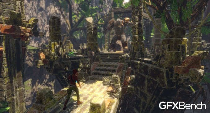
The main benchmark shown from GFXBench 5 is the Aztec Ruins scene. Kishonti notes that the benchmark has been made to scale up from phones all the way to desktops, although they focus on highlighting many of the advantages that support for Vulkan on Android will bring for games, including reducing overhead to improve CPU efficiency, which can ultimately lead to improved battery life.
As for what's new in GFXBench with Aztec Ruins, Kishonti states that the benchmark itself uses an entirely new in-house rendering engine which brings support for new effects like Dynamic Global Illumination, which is essentially a form of lighting that accounts for the illumination of certain surfaces caused by light that is reflected off of other surfaces. There are also various improvements at the engine level which take advantage of the new features included in Vulkan and other low level graphics APIs.

In addition to its use as a benchmark for typical gaming devices, GFXBench 5 will also come with a VR testing mode that measures the rendering frame rate, frame rate stability, and latency information. It will also come with a demo mode that allows users with VR headsets to explore the benchmark's Aztec Ruins environment.
GFXBench 5 is still in its development phase, and Kishonti plans to release it by Q3 of this year. It's also available for licensing within their benchmarking development program to partners and other companies that may find it relevant to their testing. For those who are at GDC or viewing the conference via streams there will also be a short demo session for the new benchmark at 6:20PM on Wednesday during the Khronos event.
More...
-
03-14-16, 06:36 PM #5816
Anandtech: AMD Announces Radeon Pro Duo: Dual GPU Fiji Video Card For VR Content Crea
At AMD’s GDC 2016 “Capsaicin” event, the company has announced their long-awaited dual Fiji video card. Being released under the name Radeon Pro Duo, the new card is a departure from the usual for AMD, with the company specifically targeting it towards VR content creation rather than end-user gaming.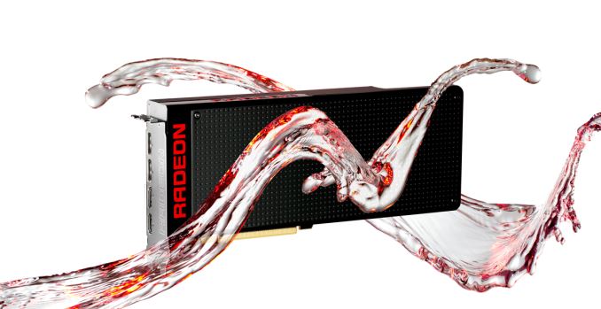
AMD originally teased their then in-development dual-Fiji card back at the Fiji launch event in June of 2015. At the time the card was expected to launch towards the end of 2015 as the company’s flagship gaming card. However at AMD’s Polaris event in December, the company announced that they were realigning the card to focus on the VR market, and would be holding it back to 2016 to launch alongside the major VR headsets.
Officially AMD’s commentary was limited reiterating their desire to have the card tied to the VR industry. However I believe that AMD also delayed the card due to the poor state of AFR scaling in recent AAA games, which would make a dual-GPU card a hard sale in the typical PC gaming market. VR, by contrast, is a much better fit since through technologies such as AMD’s affinity multi-GPU, the two perspectives that need to be rendered for VR can be mapped directly to each GPU, avoiding AFR’s dependency and pacing issues.
In any case, with the launch of the major VR headsets finally upon us, AMD is formally unveiling their dual Fiji card, the Radeon Pro Duo. That AMD is still not going after the consumer market means they have once again defied expectations, but first let’s take a look at the specs as we know them so far.
Note: AMD sent over their press release for the Radeon Pro Duo ahead of their event, with the embargo time set for the same time the event starts. Not all of the specs for the card are listed in the release, but based on the information given I believe the following to be reasonably accurate, and will be updating it with final specs as soon as they are available.
Officially, AMD promotes the Radeon Pro Duo as having 16 TFLOPS of performance; this narrows down the specifications considerably to two fully enabled Fiji GPUs, clocked at around 1GHz. Assuming the card doesn’t throttle for heat or power issues, this would put performance at an almost identical level to a Radeon R9 Fury X Crossfire, with a gap of no more than 5%.AMD GPU Specification Comparison AMD Radeon Pro Duo AMD Radeon R9 Fury X AMD Radeon R9 Fury AMD Radeon R9 295X2 Stream Processors 2 x 4096? 4096 3584 2 x 2816 Texture Units 2 x 256 256 224 2 x 176 ROPs 2 x 64 64 64 2 x 64 Boost Clock 1000MHz? 1050MHz 1000MHz 1018MHz Memory Clock 1Gbps HBM? 1Gbps HBM 1Gbps HBM 5Gbps GDDR5 Memory Bus Width 2 x 4096-bit 4096-bit 4096-bit 2 x 512-bit VRAM 2 x 4GB 4GB 4GB 2 x 4GB FP64 1/16 1/16 1/16 1/8 TrueAudio Y Y Y Y Transistor Count 2 x 8.9B 8.9B 8.9B 2 x 6.2B Typical Board Power 525W? 275W 275W 500W Manufacturing Process TSMC 28nm TSMC 28nm TSMC 28nm TSMC 28nm Architecture GCN 1.2 GCN 1.2 GCN 1.2 GCN 1.1 GPU Fiji Fiji Fiji Hawaii Launch Date Q2 2016 06/24/2015 07/14/2015 04/21/2014 Launch Price $1499 $649 $549 $1499
Otherwise as this is Fiji, the rest of the specifications should not come as a surprise. Doubling up on Fijis gives us 64 ROPs and 256 texture units per GPU. And 4GB of HBM per GPU, clocked at 1Gbps for an effective memory bandwidth of 512GB/sec.
The big unknown right now is power consumption. The shots of the card in AMD’s press materials all show 3 8-pin PCIe sockets, which would put the maximum power draw as officially allowed by the PCIe specification at 525W. However I am waiting to see what AMD confirms, as this isn’t necessarily what the card will draw. In either case, given their performance goals, such high power consumption is to be expected, as Radeon R9 Fury X was rated for 275W, and Radeon Pro Duo appears to be very close to dual Fury X in performance. This is also comparable to AMD’s previous generation dual-GPU card, the Radeon R9 295X2, which was rated for 500W.
Perhaps the bigger news though is the target market for the card. While I had initially expected AMD to target the card at the VR consumer market, AMD has gone in a different direction. Rather the Radeon Pro Duo is being pitched as a content creation card, making this an unusual halfway point between a Radeon and a FirePro.
As I’m writing this up in advance I haven’t heard AMD’s formal reasoning for why they aren’t heavily promoting it for the consumer market – though clearly the card will work there – but after giving it some thought I suspect it has to do with the system requirements for VR gaming. Both Oculus and Valve are pushing the idea that a Radeon R9 290/GeForce GTX 970 should be the performance level VR games are designed around. If developers actually follow through on this, then having a faster card is not especially useful since VR displays are locked to v-sync and can’t exceed their cap. If a 290 delivers 90fps, what would a Pro Duo when developers are targeting a fixed level of quality?
In which case content creation is the next best thing to do with the card. Games under development have yet to be tuned for performance, so it’s sound reasoning that developers would want something as fast as possible to do their initial development on. The catch for AMD is that this does limit the market for the card; besides the high price tag, the market for developers is much smaller than the market for consumers.
Finally, let’s talk pricing and availability. AMD has announced that the card will retail for $1499. This is the same price that the Radeon R9 295X2 launched at in 2014, however it’s more than double the price of a pair of Fury Xes, so pricing is arguably not aggressive there. On the other hand it’s more compact than a pair of Fury Xes (or even a pair of Nanos), so there is the space argument to be made, and as AMD’s positioning makes clear this is first and foremost a development card to begin with. Meanwhile the Pro Duo will be shipping in “early Q2 2016”, which means we should see it become available in the next one to two months.
Gallery: Radeon Pro Duo_thumb.jpg)
_thumb.jpg)
_thumb.jpg)
_thumb.jpg)
_thumb.jpg)
_thumb.jpg)
More...
-
03-15-16, 03:13 AM #5817
Anandtech: AMD Unveils GPU Architecture Roadmap: After Polaris Comes Vega
Although AMD’s GDC 2016 “Capsaicin” event was primarily focused on game development – it is the Game Developers Conference, after all – AMD did spend a brief moment discussing their future GPU plans. For the first time in many years, AMD has published a GPU architecture roadmap.
Plotting perf/watt against the years, AMD’s roadmap unveils two new architectures: Vega, and Navi. Essentially everything there is to know about these architectures is in this slide – AMD is being tight-lipped regarding further details – but this map gives us some tantalizing new information to work with.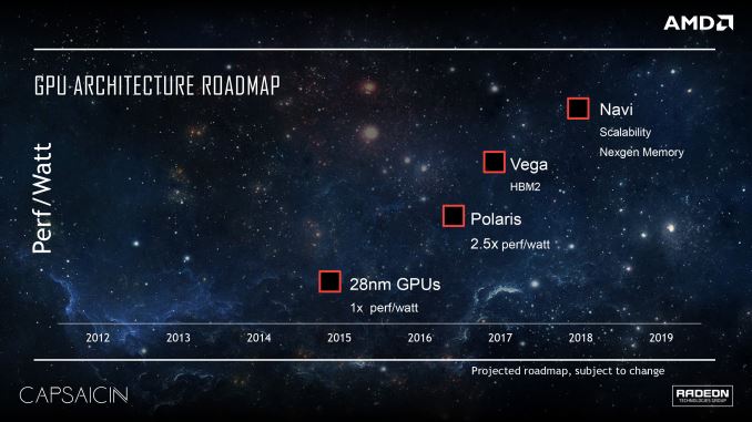
Vega is currently scheduled to come relatively quickly after Polaris. Depending on how literal you interpret this chart, the far left edge of the Vega box does fall into 2016, though obviously AMD intends to leave themselves some wiggle room here and not tie themselves down to specific dates. The fact that Vega comes this soon after Polaris is interesting; it seems hard to believe that it’s a direct successor to Polaris – I can’t see AMD replacing Polaris parts in less than a year – so this points to Vega being more of a cousin, and is where AMD’s naming system isn’t especially helpful in deciphering anything further.
With Polaris confirmed to use GDDR5, Vega is notable for being the first AMD architecture to use HBM2, and the first parts in general to use HBM tech since Fiji. I’m presuming these are higher-end GPUs to complement the Polaris GPUs (the smaller of which we know to be a low-power laptop design), which is where HBM would be more cost-effective, at least at current prices.
Meanwhile AMD has also confirmed the number of GPUs in the Vega stack and their names. We’ll be seeing a Vega 10 and a Vega 11. This follows Polaris GPU naming – which has finally been confirmed – with Polaris 10 and Polaris 11. I have also been told that Polaris 11 is the smaller of the Polaris GPUs, so at this point it’s reasonable to assume the same for Vega.
Finally, farther out towards 2018 is an architecture AMD is calling Navi. This one I suspect will attract the most attention (even if it’s the farthest out) due to the ambiguity of its features: “scalability” and “nextgen memory”. Similar to how it’s hard to see Vega directly replacing Polaris, it’s hard to see Navi directly replacing Vega after only a year. This leaves Navi rife for speculation; I could very well see it being a Polaris replacement since we’ll be nearly 2 years past Polaris, or perhaps something to do with AMD’s APU plans. Either way I don’t expect that this will be the last time AMD teases it before finally launching it.
Gallery: AMD Capsaicin Presentation Deck


More...
-
03-15-16, 09:07 AM #5818
Anandtech: The Corsair Strafe RGB Mechanical Keyboard Review with MX Silent (Red) Swi
Cherry's MX Silent switches are making their debut on the Corsair Strafe RGB gaming mechanical keyboard. Corsair has the exclusive on the MX Silent for the first year, and in this review we are examining the quality and features of the Strafe RGB keyboard as well as the performance of the new switches.
More...
-
03-15-16, 09:07 AM #5819
Anandtech: Razer Unveils The Updated Razer Blade: Chroma Keyboard, Skylake, And A Low
The 2015 Razer Blade was a nice evolution in the history of Razer’s 14-inch gaming notebook lineup. This 0.70”, or 17.8 mm thick notebook is built from a solid aluminum chassis, CNC milled and finished with a matte black finish. It is one of the thinnest and lightest gaming laptops around, and yet it still packs in a NVIDIA GTX 970M GPU. Today Razer is announcing an update to the Blade which brings some nice additions to one of the best built notebooks around.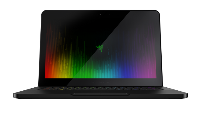
The exterior is very much the same design, which is not a bad thing. It is not identical though. Razer has shaved a bit of weight off of the package, and it is now just 4.25 lbs / 1.92 kg, down from 4.47 lbs / 2.03 kg on the previous generation. The overall finish is the same, but closer inspection reveals the addition of a USB-C port with Thunderbolt 3 as well. With Razer announcing the Razer Core external graphics dock at CES, it was a sure bet that the next Blade would also be compatible, and right on cue, Razer’s lineup which supports their external graphics dock has doubled.
Keeping to the outside, another feature which Razer debuted at CES on the Razer Blade Stealth has also found its way to the Blade, and that is the Chrome keyboard. This anti-ghosting keyboard now supports 16.8 million colors on each individual key, and it supports the Razer SDK so that games and other applications can tap in to the Chroma software to customize the lighting effects on a per-application basis. I like Razer green, but user customization trumps that color any day, and this is a welcome addition.
On the inside, there are some nice updates as well. The CPU is now an Intel Core i7-6700HQ processor, which has a 2.6 GHz base frequency and 3.5 GHz turbo, and this quad-core model also supports hyperthreading. Last year Razer bumped the memory up to 16 GB on the higher end version of the Blade, and that is now standard across the lineup, and it is of course DDR4-2133 with the inclusion of Skylake. NVIDIA hasn’t released any new GPUs in a while, and as we wait for the new FinFET graphics cards to come sometime later this year, Razer has instead moved to the 6 GB GTX 970M option, up from the 3 GB version in the Blade last year. The wireless has also been switched to the Killer Wireless-AC 1535, which can help with latency when gaming. Finally, storage has been switched out to PCIe M.2 SSDs, and for 2016 there will only be 256 GB and 512 GB options, meaning the too small 128 GB version is thankfully no more. When games can be 50 GB on their own, that simply wasn’t enough storage for this type of system.
The display is pretty much unchanged. Razer is sticking with their Sharp IGZO 3200x1800 touch display, which we’ve seen on the Blade since 2014. It is a solid panel, offering great clarity, along with good color accuracy. When I say pretty much, the one change is that the short lived 1920x1080p matte offering which lost touch capabilities, but improved battery life, is no longer available. Razer didn’t say whether this would be coming back, but they only told me they would continue listening to customer feedback. It’s possible that this model just didn’t have enough sales to justify the extra SKU.Razer Blade Comparison 2015 Razer Blade 2016 Razer Blade CPU Intel Core i7-4720HQ
quad-core 2.6-3.6GHz 22nm 47WIntel Core i7-6700HQ
quad-core 2.6-3.5GHz 14nm 47WGPU NVIDIA GTX 970M 3GB NVIDIA GTX 970M 6GB Memory 8-16 GB DDR3L-1600 16GB DDR4-2133 Display 1920x1080 IPS matte
3200x1800 IGZO touch3200x1800 IGZO touch Storage 128/256/512GB SATA M.2 256/512GB PCIe M.2 I/O 3xUSB 3.0
HDMI 1.4a3xUSB 3.0
HDMI 1.4b
USB-C Thunderbolt 3Wireless Intel Dual Band Wireless-AC 7260 Killer Wireless-AC 1535 Dimensions 13.6" x 9.3 " x 0.70"
345mm x 235mm x 17.8mm13.6" x 9.3 " x 0.70"
345mm x 235mm x 17.8mmWeight 1080p Model:
4.19 lbs / 1.9 kg
QHD+ Model:
4.47 lbs / 2.03 kg4.25 lbs / 1.93 kg Battery 70 Wh 70 Wh Keyboard Razer Green anti-ghosting Razer Chroma anti-ghosting Price $1999-$2699 $1999-$2199
Possibly the biggest change though is the pricing structure. For 2015, the lowest cost Razer Blade was the 256 GB 1080p model, for $1999, and the touch version started at $2199 for 128 GB and $2399 for 256 GB. For 2016, the entry level Blade with the QHD+ touch display and 256 GB of storage is just $1999, and the 512 GB version adds $200 to that. At the same storage capacity, Razer has lowered the price $400, and it is $500 less for the 512 GB version. That’s a significant cut, although the Razer Blade was certainly a high priced offering before. With the aggressive pricing on the Razer Blade Stealth at $999, Razer seems to be making a move to be a bigger volume player than they were in the past.
The 2016 Razer Blade will be available for pre-order on RazerZone.com tomorrow, with shipments starting in April.
Source: Razer
More...
-
03-15-16, 11:07 AM #5820
Anandtech: GDC 2016: Geomerics Demonstrates Updated Enlighten Lighting Tech
As some of our regular readers may already be familiar with them, ARM’s Geomerics division is one of the more unusual parts of ARM’s overall business group. Unlike the hardware IP ARM is best known for, Geomerics is responsible for developing and licensing technology for global illumination and indirect lighting. The group’s flagship product is Enlighten, which to date has seen use in a number of games.
This year Geomerics is at GDC to show off the latest version of Enlighten, and the latest tech demo using it, Seastack Bay. In the last year Geomerics has been focusing on improving Enlighten’s performance and abilities particularly for open world games, which require lighting on larger scales and with new technical challenges such as day/night cycles and indoor/outdoor transitions.
The latest version of Enlighten has in turn been further optimized for these scenarios. Geomerics tells us that overall lighting performance in large open world games has improved by upwards of 50%, and the company has tackled some thorny issues such as efficiently calculating indirect lighting between vertical surfaces. The latest Enlighten also has new features for landscape lighting, e.g. grass and trees.
The key technical change in the latest version is the addition of level of detail support for large terrain lighting. With upwards of 5 different levels, like other LOD implementations Enlighten’s lighting LOD allows for environments to be lit at progressively lower resolutions the farther away the terrain is. This reduces the overall rendering workload by not assigning too much CPU time to small features that are too far away to be seen. This same technology has also been implemented for light probes – specific points in a scene where lighting is calculated – allowing probes to be skipped the farther away they are.
Finally, all of this is in turn being used in the Seastack Bay tech demo being shown off at GDC. Seastack Bay is a 5km x 5km terrain chunk with a 1km beach front, specifically designed to demonstrate the new features of Enlighten. The demo was built in conjunction with Hellblade developer Ninja Theory, and is being demonstrated on both the PC and PlayStation 4.
Gallery: GDC 2016: Geomerics Enlighten


More...


 Quote
QuoteThread Information
Users Browsing this Thread
There are currently 31 users browsing this thread. (0 members and 31 guests)


Bookmarks