

Results 5,891 to 5,900 of 12096
Thread: Anandtech News
-
04-05-16, 03:00 PM #5891
Anandtech: NVIDIA Announces Tesla P100 Accelerator - Pascal GP100 Power for HPC
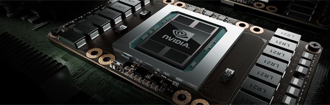
Today at their 2016 GPU Technology Conference, NVIDIA announced the first of their Pascal architecture powered Tesla cards, the Tesla P100. The P100 is the first major update to the Tesla HPC family since the launch of the first Kepler cards in late 2012, and represents a very sizable performance increase for the Tesla family thanks to the combination of smaller 16nm manufacturing process and the Pascal architecture.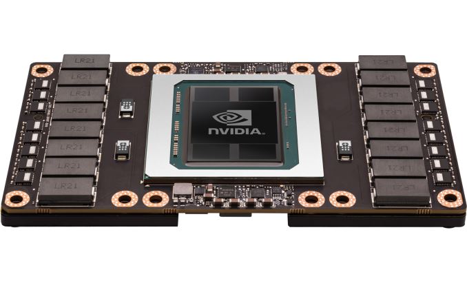
Powering the Tesla P100 is a partially disabled version of NVIDIA's new GP100 GPU, with 56 of 60 SMs enabled. GP100 is a whale of a GPU, measuring 610mm2 in die size on TSMC's 16nm FinFET process and composed of 15.3B transistors. It is remarkable in and of itself that NVIDIA and TSMC are in volume production of such a large 16nm die at this time, as everything else we've seen with a confirmed size is at best one-quarter of this size. GP100 is being produced on TSMC's Chip-On-Wafer-On-Substrate technology, with this line apparently being used for putting the GPU and HBM2 DRAM stacks on the same interposer.NVIDIA Tesla Family Specification Comparison Tesla P100 Tesla K80 Tesla K40 Tesla M40 Stream Processors 3584 2 x 2496 2880 3072 Core Clock 1328MHz 562MHz 745MHz 948MHz Boost Clock(s) 1480MHz 875MHz 810MHz, 875MHz 1114MHz Memory Clock 1.4Gbps HBM2 5GHz GDDR5 6GHz GDDR5 6GHz GDDR5 Memory Bus Width 4096-bit 2 x 384-bit 384-bit 384-bit Memory Bandwidth 720GB/sec 2 x 240GB/sec 288GB/sec 288GB/sec VRAM 16GB 2 x 12GB 12GB 12GB Half Precision 21.2 TFLOPS 8.74 TFLOPS 4.29 TFLOPS 6.8 TFLOPS Single Precision 10.6 TFLOPS 8.74 TFLOPS 4.29 TFLOPS 6.8 TFLOPS Double Precision 5.3 TFLOPS
(1/2 rate)2.91 TFLOPS
(1/3 rate)1.43 TFLOPS
(1/3 rate)213 GFLOPS
(1/32 rate)GPU GP100
(610mm2)GK210 GK110B GM200 Transistor Count 15.3B 2 x 7.1B(?) 7.1B 8B TDP 300W 300W 235W 250W Cooling N/A Passive Active/Passive Passive Manufacturing Process TSMC 16nm FinFET TSMC 28nm TSMC 28nm TSMC 28nm Architecture Pascal Kepler Kepler Maxwell 2
We'll dive into the full Pascal architecture (as implemented by GP100) at a later time, but it's worth noting that Pascal here is 64 FP32 CUDA cores per SM, versus 128 on Maxwell. Each of those SMs also contains 32 FP64 CUDA cores - giving us the 1/2 rate for FP64 - and new to the Pascal architecture is the ability to pack 2 FP16 operations inside a single FP32 CUDA core under the right circumstances. With a boost clock of 1.48GHz, altogether Tesla P100 will offer 10.6 TFLOPS of FP32 performance or 5.3 TFLOPS of FP64 performance, more than doubling and tripling Tesla K40's rated throughput on these metrics respectively. NVIDIA has been happy to crow about the performance of Tesla P100, and for good reason, as this stands to be a very powerful processor.
Paired with the GP100 GPU on Tesla P100 is 16GB of HBM2 VRAM, laid out in 4 stacks for a 4096-bit memory bus. NVIDIA quotes P100 as offering 720GB/sec of memory bandwidth, which works out to a memory clock of 1.4Gbps. As we've seen with other HBM products, this marks a significant increase in memory bandwidth, more than doubling NVIDIA's last generation of cards.
In their announcement, NVIDIA also confirmed that Tesla P100 will support NVLink, with 4 NVLink controllers. Previously announced, NVLink will allow GPUs to connect to either each other or to supporting CPUs (OpenPOWER), offering a higher bandwidth cache coherent link than what PCIe 3 offers. This link will be important for NVIDIA for a number of reasons, as their scalability and unified memory plans are built around its functionality.
Speaking of functionality, Tesla P100 and the underlying GP100 GPU is a full-featured HPC GPU. It supports all of the HPC-centric functionality that the Tesla K20/40/80 embodied, including ECC memory protection for the register file, caches, and HBM2 DRAM. Coupled with the very high FP64 rate, and it's clear that this is the successor of the GK110/GK210 GPU.
NVIDIA's pictures also confirm that this is using their new mezzanine connector, with flat boards no longer on perpendicular cards. This is a very HPC-centric design (I'd expect to see plenty of PCIe cards in time as well), but again was previously announced and is well suited for the market NVIDIA is going after, where these cards will be installed in a manner very similar to LGA CPUs. The P100 is rated for a TDP of 300W, so the cooling requirements are a bit higher than last-generation cards, most of which were in the 230W-250W range.
Finally, in its initial implementation NVIDIA is focusing on customers that need extreme scaling capabilities, and I wouldn't be too surprised if this was in part due to the margins of that market and how these initial cards will be in demand. NVLink of course plays a big part here, with NVIDIA able to go up to 8-way configurations thanks to it.
Gallery: NVIDIA Tesla P100


More...
-
04-06-16, 02:12 AM #5892
Anandtech: Vivaldi Web Browser Launches With Version 1.0: Built For Power Users Of Th
Today, Vivaldi has gone from a beta project to a production web browser with the official launch of version 1.0. After more than a year in public development, the team led by Opera Software co-founder Jon Stephenson von Tetzchner is ready to release their take on the modern browser with this first release. They are calling it a new browser for the web’s most demanding users, and they are trying to build an approach that focuses on the tasks that people want to do on the web.
The company has looked at the approaches by the other major browser makers, and seen a move towards simplification of their interfaces. With Vivaldi, the team wants to bring back features that have been dropped over the years, as well as create new functionality that doesn’t exist today, or perhaps needs extensions added to the browser to work. I use Microsoft Edge and Google Chrome as my two primary browsers, and both of them have been lacking for me in different ways, so I took the final release version of Vivaldi for a brief spin.
Vivaldi is built on the Blink layout engine, which is part of the Chromium project and the layout engine used by Google’s Chrome browser. But Vivaldi adds a lot of functionality right out of the gate, with a wide range of features consolidated into the basic install, and with the ability to customize the browser to your own liking as one of the key goals of the project.
The customizability is apparent from the first install. Right away the install asks several questions about tab layout, looks, and more, before diving into the web itself. Once up and running, you can go into the settings and configure a huge array of options, including changing the tab locations, startup, appearance, and privacy. There are literally too many settings to go through here, but the end result is quite a bit of choice for the end user, and that’s a good thing.
Vivaldi also has some great features for managing the web and customizing your workflow. It includes Tab Stacks, and you can set that up by just dragging a tab onto another one, and then you can access each stacked tab with keyboard shortcuts or by clicking the top of the stack. It also has Tab Stack Tiling, allowing you to display multiple pages at the same time, with multiple tab stacks. You can also set websites up as Web Panels, giving you a smaller slice of the website pinned to the side. This works great for things like Twitter, and lets you monitor it while having another page up in the main area. Mobile responsive sites will also nicely collapse into these web panels.
Vivaldi also features the ability to save web sessions, and you can then open the entire session at once to get back to work quickly. If you need to jot something down quickly, it features built-in notes as well. Navigation can be done quickly with a fast forward and rewind function, with fast forward taking you to the next logical page of the site you are on, and rewind takes you back to the first page you browsed to if you’ve gone to several pages on a site.
Since this browser is built for the power user, it also features a large list of keyboard shortcuts to keep your hands ready for typing, and in addition it also supports a pretty big list of mouse gestures, which can be accessed by holding the right mouse button. For example, you can go back and forward with just a mouse gesture by holding the right mouse and gesturing left or right. For those with a trackpad, you can optionally enable holding the Alt key to enable the same features on a trackpad.
The user interface for Vivaldi is built around the same web technologies that it renders, such as HTML 5, node.js, and more. The interface can do nifty things like automatically change colors based on the page you are on.
One of the nicest little features I've already noticed is that Vivaldi will show you the size of a web page in the address bar as it loads, giving you a nice little glimpse at just how much data you are pulling in on a single page.
I’ve tested Vivaldi on a high DPI display, and both the installer and browser itself seems to adapt very well to higher resolution displays, at least on Windows. It wasn’t always the case earlier in the preview stages for the browser, so the team has done some nice work to get this sorted out.
I’m not sure if the world is ready for yet another web browser, but the Vivaldi product seems to pack in a pretty impressive set of features, along with a nice looking interface with plenty of customizability. As someone who has been somewhat disappointed in the browsers I’ve been using, Vivaldi is going to get some screen time on my PCs and we’ll see how it handles day to day use. Being based on Blink should be a good start for things like page layout and performance, but with more functionality built in than you get out of the box on Chrome.
If you want to give Vivaldi a spin, check it out here:
https://vivaldi.com/
More...
-
04-06-16, 07:23 AM #5893
Anandtech: NVIDIA Unveils the DGX-1 HPC Server: 8 Teslas, 3U, Q2 2016
For a few years now, NVIDIA has been flirting with the server business as a means of driving the growth of datacenter sales of their products. A combination of proof-of-concept hardware configurations and going into spaces not necessarily served right away by the OEMs, NVIDIA has over the years put together boxes like their Quadro Visual Computing Appliance and the DIGITS devbox. Though a side business for NVIDIA, it’s one that has taken on some importance, and nowhere is this more applicable than with the Pascal-based Tesla P100 announced this week._575px.jpg)
One of the more interesting aspects we’ve known about P100 for some time now – and well before the product was formally announced this week – was that NVIDIA would be pursuing a new form factor and new interconnect technology. Though the GP100 GPU at the heart of the P100 supports traditional PCI Express, NVIDIA has also invested heavily in NVLink, their higher-speed interconnect to enable fast memory access between GPUs, and unified memory between the GPU and CPU. For NVIDIA this is a logical progression: as GPUs become increasingly CPU-like in their flexibility and necessity, they move from being a peripheral to a core processor, and so too must their I/O and form factor evolve to match.
This brings us back to servers. Because NVIDIA is launching P100 with a new form factor and connector, P100 requires completely new infrastructure to run. NVIDIA’s OEM partners will in successive quarters be offering their own systems supporting P100 and its mezzanine connector, but right now at day 1 there is nothing from the OEMs ready to support P100. So in order to avoid the long gap for OEM servers to catch up, to serve as a pathfinder for their own development of P100 and its software, and to further their own goals for the server market, NVIDIA is producing their own P100 server – the first P100 server – the full scale DGX-1.
I call DGX-1 a full-scale server because it is a maximum implementation of Tesla P100 right off the bat. 8 P100s are installed in a hybrid mesh cube configuration, making full use of the NVLink interconnect to offer a tremendous amount of memory bandwidth between the GPUs. Each NVLink offers a bidirectional 20GB/sec up 20GB/sec down, with 4 links per GP100 GPU, for an aggregate bandwidth of 80GB/sec up and another 80GB/sec down.
The mesh itself is a Non-Uniform Memory Access (NUMA) style design; with 4 links, not every GPU can be linked to every other GPU. But in the case where two GPUs aren’t linked, the next GPU is no more than 1 hop away. Meanwhile, the GPUs connect back to their x86 CPU host over standard PCI Express.
NVLink in turn enables each GPU to directly execute read, write, and atomic memory operations out of the memory of the other GPUs, functionality that has not been available to NVIDIA GPUs before. For this reason, NVIDIA has not shied away from pointing out that while NVLink may technically be an interconnect, it’s really more of a memory technology, which would make data transference one such application of the technology. Fundamentally this ends up being a very different take on an interconnect than PCI Express, which is a data bus with certain memory-like features layered on top of it. In this case it’s probably safe to say that NVLink is closer to the likes of Intel’s QPI and AMD’s HyperTransport.
Getting back to the server itself, backing up the P100s is a hefty dual Intel Xeon based system. The DGX-1’s 3U chassis holds a dual 16-core Xeon E5-2698 v3 arrangement, 512 GB of DDR4-2133 LRDIMMs, four Samsung PM863 1.92 TB storage drives, dual 10 gigabit Ethernet (10GBase-T) as well as four EDR Infiniband connections. This system serves not only to feed the Teslas, but to further drive home NVIDIA’s scalability goals as well, with the Infiniband connections in particular put in place to allow for high-performance DGX-1 clusters. Of course with so much hardware on hand you’ll need a lot of power to drive it as well – 3200W, to be precise – as the 8 P100s alone can draw up to 2400W.
In terms of construction, as hinted by in NVIDIA’s sole diagram of a component-level view of the DGX-1, the Tesla cards sit on their own carrier board, with the Xeon CPUs, DRAM, and most other parts occupying their own board. The carrier board in turn serves two functions: it allows for a dedicated board for routing the NVLink connections – each P100 requires 800 pins, 400 for PCIe + power, and another 400 for the NVLinks, adding up to nearly 1600 board traces for NVLinks alone – and it also allows easier integration into OEM designs, as OEMs need only supply an interface for the carrier board. It’s a bit of an amusing juxtaposition then, as the carrier board essentially makes for one massive 8 GPU compute card, being fed with PCIe lanes from the CPU and power from the PSU.NVIDIA DGX-1 Specifications CPUs 2x Intel Xeon E5-2698 v3 (16 core, Haswell-EP) GPUs 8x NVIDIA Tesla P100 (3584 CUDA Cores) System Memory 512GB DDR4-2133 (LRDIMM) GPU Memory 128GB HBM2 (8x 16GB) Storage 4x Samsung PM863 1.92TB SSDs Networking 4x Infiniband EDR
2x 10GigEPower 3200W Size 3U Rackmount GPU Throughput FP16: 170 TFLOPs
FP32: 85 TFLOPs
FP64: 42.5 TFLOPs
On a quick aside, I also asked NVIDIA about cooling for the P100s, given that there’s 2400W of them to cool. While they aren’t going into great detail about the heatsinks used (e.g. whether there are any vapor chambers involved), they did confirm that they are 2U tall heatsinks, and as NVIDIA is wont to do, the tops are painted green. Apparently these are the standard heatsinks for P100, and when OEMs start assembling their own systems, these will be the heatsinks that come with the boards.
Meanwhile, besides the practical necessity of constructing the DGX-1 as the pathfinder system and reference implementation for the P100, at the end of the day the DGX-1 is meant to be a workhorse for NVIDIA’s customers. Given its 8 P100s we’re looking at 28,672 CUDA cores and 128GB of shared VRAM, the DGX-1 is rated to be able to hit 170 FP16 TFLOPs of performance (or 85 FP32 TFLOPs) inside of 3Us. And though the server should be good at just about any HPC task given the versatility offered by the P100 – it offers fast FP64 and ECC as well – NVIDIA is initially pitching the box at the deep learning/neural network market, where they’re intending to fully exploit the FP16 performance improvements of the Pascal architecture. NVIDIA has of course been building towards this market for some time now, and it is their hope that DGX-1 combined with their ever-increasing collection of tools and SDKs (cuDNN, DIGITS, etc) that this will serve as a catalyst for that market.
The same can be said as well about the server space in general. Producing their own server does put NVIDIA in competition with their OEM partners to some degree, but in chatting with NVIDIA they have made it very clear that this isn’t a long-term strategy – that they don’t want to be a full-fledged server vendor. Rather the DGX-1 is the tip of the spear as the first P100 system, and is meant to create and spur on the market, which is where the OEMs will step in next year with their own, far larger variety of systems.
In the meantime, with OEM Tesla P100-equipped systems not set to ship until Q1 of 2017, for the next couple of quarters the DGX-1 will be the only way for customers to get their hands on a P100. The systems will be production quality, but they are nonetheless initially targeted at early adopters who want/need P100 access as soon as possible, with a price tag to match: $129,000.
It goes without saying that NVIDIA seems very confident that they’ll sell plenty of systems at this price, and while it’s not being said by anyone at NVIDIA, I think it’s reasonable to assume that the high price tag is the tradeoff customers will have to make to get P100 so soon. The underlying (and massive) GP100 GPU is in full volume production, but it’s difficult to imagine chip yields are spectacular, even for the cut-down 56 SM configuration used on P100. Rather it’s that NVIDIA is willing to go into volume production now and sell GP100-based products so early because HPC customers will pay such a high price, essentially eating the cost of low yields in order to get the good GPUs that come out of TSMC ASAP.
Anyhow, NVIDIA has already begun taking pre-orders of the systems over on their website. The first systems will be shipping in May to various research universities; what NVIDIA calls their pioneers. After that, DGX-1 boxes will begin shipping to their close partners and customers in the rest of Q2. Notably (and a bit surprisingly), Q2 not only includes NVIDIA’s close partners, but general pre-order customers as well. So for those customers who got their pre-orders in early enough yesterday to get one of the first servers, they should be able to get their hands on DGX-1 and the Tesla P100s inside by the end of June.
More...
-
04-06-16, 09:08 AM #5894
Anandtech: Huawei Launches the TalkBand B3
I’ve been using the TalkBand B2 for a couple of months (a write-up will come soon), and Huawei is announcing the release of their TalkBand B3. This is a pseudo smartwatch, or ‘minimalist wearable device’, that goes on the wrist and tracks steps, calories, sleep patterns, runs and cycling events. This data is then shared via a Huawei app.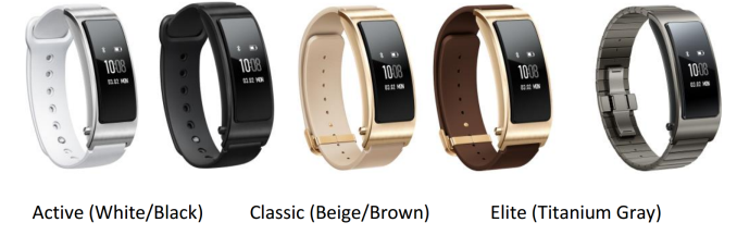
The B3 is a hardware upgrade as well as a visual upgrade over the B2. In either the Active, Classic or Elite styles, using higher grade stainless steel and Italian leather for the strap. The same concept of the B2 is in play – a curved screen in a removable module, making it easy enough to charge or change straps. The display is a PMOLED at 80x128 capable of monochrome images and text, and the watch vibrates on notifications with specific apps. As the name ‘TalkBand’ suggests, it can be used to take calls and respond to the caller through the integrated speaker and microphone.
The 91 mAh battery is listed by Huawei as supporting up to 6 hours of calling, a 3-4 day battery life, and a 1.5 hour charge. Currently my B2 can’t go more than a couple of days without a charge, so hopefully this should be an improvement. A feature I like is the ability to set a time period for wake-up: the TalkBand will detect when you are in a light sleep (rather than deep sleep) period and vibrate to wake you up without waking your spouse.
The B3 is IP57 rated, with the Active version available in White/Black for 169 Euro, the Classic in Beige/Brown for 199 Euro, and the Elite in Titanium Grey for 249 Euro. The pricing differential is derived from the color and strap design. At that price Huawei will be competing with some of the cheaper full-Android smart watches, although a trade-off will be utility with battery life.
More...
-
04-06-16, 09:08 AM #5895
Anandtech: Huawei Launches The P9 and P9 Plus
Today in London, Huawei has launched the latest devices in its P-series line. The P9 and P9 Plus take cues from the previous P8 but also some hardware moves over from the Mate 8 in the form of the SoC base design. The two models come in various memory and storage variants to the EU and Asia, though some colors and high-end storage configurations will be Asia only.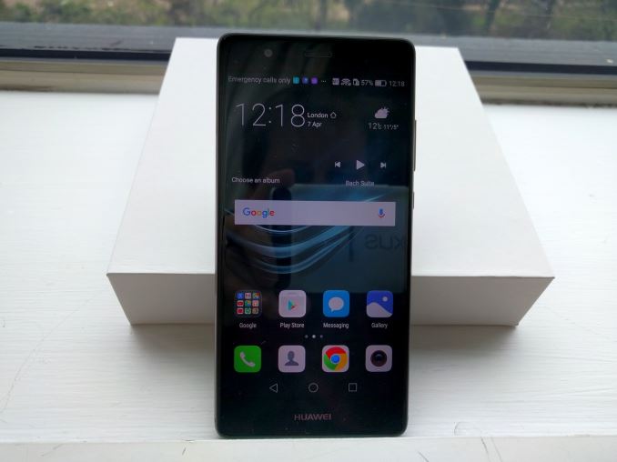
The new P9 and P9 Plus are aluminium unibody designs, with the two main features being the new Kirin 955 SoC and the Dual Camera design on the rear with Leica certification. The way Huawei is using the dual camera design is different to previous dual camera smartphones from other companies – one is a color camera and the other is a black and white camera. This allows several advances over a standard one camera design.
Firstly, having black-and-white data means that the grey contrast of an image can be optimized depending on the shot itself. The B/W camera also has fewer color filters in the lens design, allowing for 2x light into the sensor over the color camera, giving an equivalent light data of 3x a single camera design. Thirdly, with two cameras and a separation, based on the contrast data Huawei can use an ISP to attempt triangulation of distance. This allows the integrated software to implement a simulated focal length of F/0.95 to F/16, giving bokeh type effects. This is not a true bokeh, but in the three minutes I played around with the device it did give a similar effect. Both cameras are 12MP, running 1.25 micron pixels and a base F/2.2 aperture. There is a laser autofocus on the P9, but no OIS.Huawei P9 & P9 Plus Model P9 P9 Plus SoC HiSilicon Kirin 955
4x Cortex A53 @ 1.8GHz
4x Cortex A72 @ 2.5GHz
Mali-T880MP4 @ 900MHz (?)RAM 3 LPDDR3 @ ? MHz / 4GB LPDDR4 @ 1333MHz NAND 32GB / 64GB / 128GB (later) NAND
+ microSDDisplay 5.2” 1080p IPS LCD 5.5” 1080p AMOLED Modem 2G/3G/4G LTE Cat 6
(Integrated HiSilicon Balong Modem)Dimensions 145.0 (H) x 70.9 (W) x 6.95mm (D)
144g weight152.3 (H) x 75.3 (W) x 6.98mm (D)
162g weightCamera Dual Rear Camera (RGB + Monochrome)
2x 12MP ( X × Y)
w/ 1.25µm pixels
F/2.2 aperture, x mm eq.Front Facing Camera
8MP ( 3264 × 2448 )
Sony IMX179 1/3.2" w/ 1.4µm pixels
F/2.4 aperture, 26mm eq.Battery 3000mAh 3400mAh OS Android 6.0
with EmotionUI 4.1Connectivity 802.11a/b/g/n/ac dual-band 2.4 & 5GHz
BT 4.2, USB-C, GPS/GNSS,
DLNA, NFCSIM Size NanoSIM +
NanoSIM (w/o microSD)MSRP 3GB + 32GB Europe: 599€ 4GB + 64GB Europe:649€ 4GB + 64GB Europe:749€
The cameras are Leica certified. The partnership with Leica was announced earlier in the year, but this means that the sensors and lenses pass Leica’s internal tests for color accuracy and reproduction. At this time we were unable to find out who exactly makes each of the sensors, although when we get the device in house (hopefully after the press event today) we can find out. Leica’s partnership also extends to the software, allowing the new camera features to be used.
Gallery: Huawei P9


Both the P9 and P9 Plus have the same camera arrangement and underlying Kirin 955 SoC. This is an upgrade over the Kirin 950 we saw in the Huawei Mate 8, with increased clock speeds (+200MHz on the A72 cores to reach 2.5GHz) and upgraded ISP/DSPs in silicon. HiSilicon states that power efficiency has seen an improvement over the Kirin 950, which should result in outstanding battery life for the P9.
The difference between the P9 and P9 Plus will be in several areas. Both devices are 1920x1080 (FHD) resolution, with the P9 at 5.2-inch and the P9 Plus at 5.5-inch. The P9 Plus will use a Super AMOLED display, with the P9 being a standard IPS but with 69% DCI-P3 gamut. The DRAM/storage configurations will be different as well. The P9 will be available in 3GB/32GB and 3GB/64GB variants (LPDDR3, eMMC), with a 4GB/128GB variant coming to Asia in the future (LPDDR4). The P9 Plus by contrast will have a base 4GB/64GB model, again with a 128GB model for Asia.
The P9 Plus in all variants will feature Huawei’s Force Touch technology, as seen on the Mate S 128GB version, however we are told that the utility of the feature will have increased beyond picture zoom and weighing fruit. Also, the EU will have the Mystic Silver and Titanium Grey colors only, while Asia also gets the Rose Gold and Haze Gold variants.
Both the P9 and P9 Plus will use USB Type-C, with Asian versions supporting Dual SIM functionality. The P9 battery runs at 3000 mAh compared to the P9 Plus at 3400 mAh, with both devices listed as 1.5-day battery run time. Both devices feature the same fingerprint sensor from the Mate 8, with the P9 Plus having an IR blaster as well. Both devices (in our quick hands on) ran Huawei’s customized EMUI 4.1 interface, which is reminiscent of iOS. Both devices also support knuckle interactions, similar to the Mate S.
Pricing for the 3GB/32GB and 4GB/64GB models of the P9 comes in at 599€ and 649€, while the P9 Plus in its 4GB/64GB variant comes at 749€. The P9 should hit the shelves in April, with the P9 Plus in May. 128GB variants for Asia will be slightly later than the smaller storage implementations.
More...
-
04-06-16, 11:07 AM #5896
Anandtech: IBM, NVIDIA and Wistron Develop New OpenPOWER HPC Server with POWER8 CPUs
IBM, NVIDIA and Wistron have introduced their second-generation server for high-performance computing (HPC) applications at the OpenPOWER Summit. The new machine is designed for IBM’s latest POWER8 microprocessors, NVIDIA’s upcoming Tesla P100 compute accelerators (featuring the company’s Pascal architecture) and the company’s NVLink interconnection technology. The new HPC platform will require software makers to port their apps to the new architectures, which is why IBM and NVIDIA plan to help with that.
The new HPC platform developed by IBM, NVIDIA and Wistron (which is one of the major contract makers of servers) is based on several IBM POWER8 processors and several NVIDIA Tesla P100 accelerators. At present, the three companies do not reveal a lot of details about their new HPC platform, but it is safe to assume that it has two IBM POWER8 CPUs and four or eight NVIDIA Tesla P100 accelerators. Assuming that every GP100 chip has four 20 GB/s NVLink interconnections, four GPUs is the maximum number of GPUs per CPU, which makes sense from bandwidth point of view. Keeping in mind that it is possible to install eight Tesla P100 into a 2P server (see the example of the NVIDIA DGX-1), the new HPC platform by IBM could do just that. Still, even with four Tesla P100 accelerators the systems would offer a rather formidable performance.
IBM’s POWER8 CPUs have 12 cores, each of which can handle eight hardware threads at the same time thanks to 16 execution pipelines. The 12-core POWER8 CPU can run at fairly high clock-rates of 3 – 3.5 GHz and integrate a total of 6 MB of L2 cache (512 KB per core) as well as 96 MB/s of L3 cache. Each POWER8 processor supports up to 1 TB of DDR3 or DDR4 memory with up to 230 GB/s sustained bandwidth (by comparison, Intel’s Xeon E5 v4 chips “only” support up to 76.8 GB/s of bandwidth with DDR4-2400). Since the POWER8 was designed both for high-end servers and supercomputers in mind, it also integrates a massive amount of PCIe controllers as well as multiple NVIDIA’s NVLinks to connect to special-purpose accelerators as well as the forthcoming Tesla compute processors.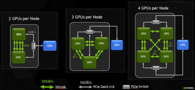
Each NVIDIA Tesla P100 compute accelerator features 3584 stream processors, 4 MB L2 cache and 16 GB of HBM2 memory connected to the GPU using 4096-bit bus. Single-precision performance of the Tesla P100 is around 10.6 TFLOPS, whereas its double precision is approximately 5.3 TFLOPS. A HPC node with eight such accelerators will have a peak 32-bit compute performance of 84.8 TFLOPS, whereas its 64-bit compute capability will be 42.4 TFLOPS. Just for comparison: NEC’s Earth Simulator supercomputer, which was the world’s most powerful system from June 2002 to June 2004, had a performance of 35.86 TFLOPS running the Linpack benchmark. The Earth Simulator consumed 20 kW of POWER, it consisted of 640 nodes with eight vector processors and 16 GB of memory at each node, for a total of 5120 CPUs and 10 TB of RAM. Thanks to Tesla P100, it is now possible to get performance of the Earth Simulator from just one 2U box.
IBM, NVIDIA and Wistron expect their early second-generation HPC platforms featuring IBM’s POWER8 processors to become available in Q4 2016. This does not mean that the machines will be deployed widely from the start. At present, the majority of HPC systems are based on Intel’s or AMD’s x86 processors. Developers of high-performance compute apps will have to learn how to better utilize IBM’s POWER8 CPUs, NVIDIA Pascal GPUs, the additional bandwidth provided by the NVLink technology as well as the Page Migration Engine tech (unified memory) developed by IBM and NVIDIA. The two companies intend to create a network of labs to help developers and ISVs port applications on the new HPC platforms. These labs will be very important not only to IBM and NVIDIA, but also to the future of high-performance systems in general. Heterogeneous supercomputers can offer very high performance, but in order to use that, new methods of programming are needed.
The development of the second-gen IBM POWER8-based HPC server is an important step towards building the Summit and the Sierra supercomputers for Oak Ridge National Laboratory and Lawrence Livermore National Laboratory. Both the Summit and the Sierra will be based on the POWER9 processors formally introduced last year as well as NVIDIA’s upcoming code-named Volta processors. The systems will also rely on NVIDIA’s second-generation NVLink interconnect.
More...
-
04-07-16, 08:06 AM #5897
Anandtech: The ASUS Maximus VIII Extreme Review: The Other $500 Option
On the back of our last $500 motherboard review, it was clear that a number of readers were surprised that a mainstream motherboard could cost so much. We took the opportunity to ask ASUS why such a thing exists, especially when a high-end desktop platform combination could cost less. The answer is due to the engineering: an ROG motherboard takes twice as long to design and validate, as well as custom ICs and finding the secret sauce to each platform. ASUS said that they have platforms for any budget, but for the users who want to squeeze every last morsel of performance in a mainstream halo budget, they have a product for that as well. That product is the Maximus VIII Extreme, and this is our review.
More...
-
04-07-16, 08:06 AM #5898
Anandtech: Tyan Introduces 1U POWER8-Based Server for HPC, In-Memory Applications
At this week's OpenPOWER Summit in San Jose, California, Tyan has introduced its new IBM POWER8-based 1U servers designed for high-performance computing (HPC) as well as in-memory applications. The new machines are designed to target niche markets that do not require extreme processing performance, but need a lot of RAM. The new Tyan GT75 expands the range of Tyan’s POWER8-based machines and helps IBM’s POWER8 platform to compete against Intel Xeon in niche markets.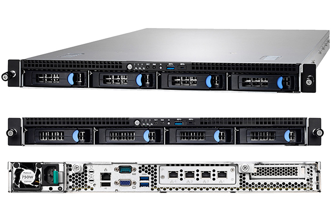
Nowadays over 95% of servers are based on Intel’s Xeon microprocessors, which does not make producers of servers and operators of large datacenters happy because they have one supplier of key components that controls platform development and prices. Three years ago, IBM teamed up with Google, Mellanox, NVIDIA and Tyan to establish the OpenPOWER Foundation to develop servers based on IBM’s processors collaboratively. So far, IBM POWER-based servers have not gained a lot of market share, but it looks like they are starting to gain traction as companies like Tyan are expanding their POWER8 hardware offerings.
The Tyan GT75 machines (just like the Tyan TN71-BP012 servers launched a year ago) are based on one IBM POWER8 Turismo SCM processor with eight or ten cores and can be equipped with up to 1 TB of memory. The systems feature 32 R-DDR3L DIMM slots using four IBM Centaur memory buffer chips (MBCs) and support 32 GB modules, which are considerably more affordable than 64 GB or 128 GB memory sticks.
While the GT75 servers (BSP012G75V4H) feature only one CPU, each IBM POWER8 core can process up to eight hardware threads simultaneously thanks to 16 execution pipelines. The chips also have massive caches (512 KB L2 per core, 8 MB eDRAM L3 per core as well as 16 MB per MBC), which are particularly useful for memory-intensive applications.Comparison of IBM POWER8 Turismo CPUs Compatible with
Tyan's SC75 and TN71 ServersPOWER8 8-Core POWER8 10-Core POWER8 12-Core Core Count 8 10 12 Threads 64 80 96 Frequency (nominal) 2.328 GHz
3.325 GHz2.095 GHz
2.926 GHz2.561 GHz L2 Cache 512 KB per core
2 MB per CPU512 KB per core
5 MB per CPU512 KB per core
6 MB per CPUL3 Cache 8 MB eDRAM per core
64 MB per CPU8 MB eDRAM per core
80 MB per CPU8 MB eDRAM per core
96 MB per CPUDRAM Interface DDR3L-1600, memory connects to CPUs using the IBM Centaur MBCs PCI Express 3 × PCIe controllers, 32 lanes TDP 130W
190W130W
190W190W
The Tyan GT75-BP012, which is a 1U server that is designed for in-memory computing, HPC and virtualization, can be equipped with up to four 3.5” hot-swappable SAS 12G/SATA 6G HDD/SSDs, four network controllers (1 GbE and 10 GbE) as well as a 750 W PSU. The server uses the PLX PEX8748 PCIe switch and one PCIe 3.0 x8 expansion slot. Tyan did not reveal the price of the system, but said that it would be available already in April.Comparison of Tyan GT75 Servers BSP012G75V4H-B4C BSP012G75V4H-Q4T BSP012G75V4H-Q4F CPU IBM POWER8
8-Core
2.328 GHz
130 W/169 W TDPIBM POWER8
10-Core
2.095 GHz
130 W/169 W TDPIBM POWER8
10-Core
2.095 GHz
130 W/169 W TDPInstalled RAM 8 × 16 GB R-DDR3L 16 × 16 GB R-DDR3L 32 × 16 GB R-DDR3L RAM (subsystem) Up to 1 TB of DDR3L-1333 DRAM, 32 RDIMM modules, four IBM Centaur MBCs Storage 2 × 512 GB SSDs 2 × 1 TB SSDs 4 × 1 TB SSDs Tyan Storage Mezzanine MP012-9235-4I
(4-port SATA 6Gb/s IOC w/o RAID stack)LAN 4 × GbE ports 4 × 10 GbE ports 4 × 10 GbE ports Tyan LAN Mezzanine MP012-5719-4C
Broadcom 1GbE LAN Mezz CardMP012-B840-4T
Qlogic+Broadcom 10GbE LAN Mezz Card-MP012-Q840-4F Qlogic 10GbE LAN Mezz Card
The new 1U machines complement the Tyan TN71-BP012 launched in March, 2015. The TN71 is a 1-way 2U platform for data analytics and applications, it supports 12 3.5” hot-swappable SAS 12G/SATA 6G HDD/SSDs, four 10 GbE network ports as well as two 1200 W PSUs for redundancy reason. This machine supports IBM POWER8 Turismo SCM processor with up to 12 cores and is generally more powerful than the GT75.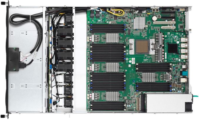
More...
-
04-07-16, 10:24 AM #5899
Anandtech: 3DMark Adds VRMark Preview and an Updated UI
We now have the release of the high end consumer VR headsets behind us. That sets the stage for a (hopefully) steady flow of software to use with the new (and future) headsets. Among the latest announcements is the inevitable release of a benchmark from Futuremark, who has long been a staple in PC gaming benchmarks. Their latest update brings a new VR experience, an updated user interface, and control over benchmark downloads and updates.
FutureMark’s latest release is an interactive preview of VRMark, which is now available for the 3DMark Advanced and Professional editions. In this preview users are allowed to freely explore two test scenes with the Oculus Rift, HTC Vive, and of course a standard monitor.
Both scenes included take place in an exhibit room of a museum and feature scenes from benchmarks in years past. With this preview of tests to come the first scene is geared toward the minimum level specifications we have seen outlined for both the HTC Vive and Oculus Rift, with scene two targeting more powerful hardware. No scores are given by either demo, but they both ran smooth on a Titan X running a G-Sync monitor. Though I would have to jump in with a headset to really see how demanding this preview is to run.
To coincide with the release of the VRMark preview, FutureMark is also updating the user interface of 3DMark as a whole. When the 3DMark suite is first started up a new home screen recommends a test based on the configuration of the system. On a deeper level all benchmarks are now downloaded on an individual basis and can be updated independently as well. Which can help avoid large downloads every time there is an update.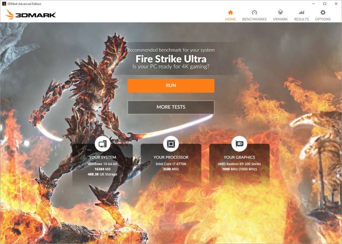
Alongside all of this news Ice Storm Extreme and Ice Storm Unlimited are now unlocked in 3DMark Basic Edition. Additionally, SystemInfo has been updated to version 4.43, bringing with it improved hardware detection. FutureMark also states that their next major update will bring us the new Time Spy benchmark which features DirectX 12. For more information about VRMark see Futuremarks VRMark landing page.
More...
-
04-07-16, 01:00 PM #5900
Anandtech: Samsung Begins To Produce DDR4 Memory Using '10nm Class' Process Tech
Samsung Electronics has started to manufacture DDR4 memory using its new '10nm class' production technology. '10nm class', by definition, implies sub-20nm but without fully disclosing the methodology, similar to the first sub-20nm NAND production that used 1x/1y terminology. By using a sub-20 nm fabrication process, this typically helps a company make ICs/DRAM cheaper, faster and more energy efficient, depending on the process complexity. In this case, Samsung continues to use ArF (argon fluoride) immersion lithography tools with quadruple patterning to make its latest memory, which indicates a very high complexity of the new process tech. What is also important is that the new DRAMs feature Samsung’s new memory cell structure.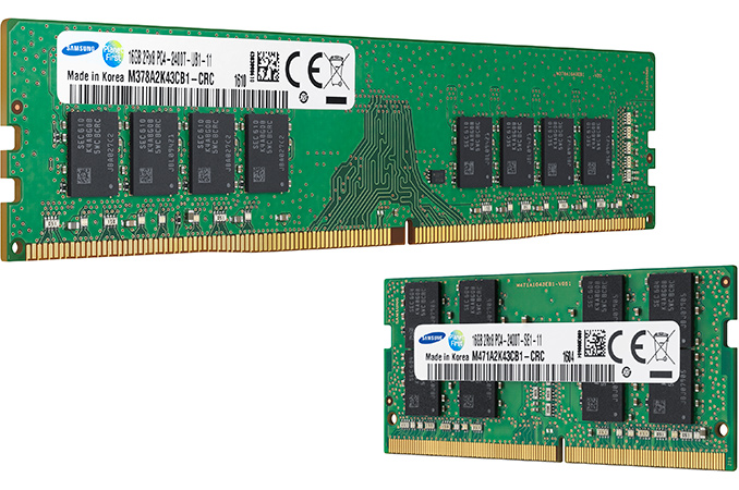
In the news today, Samsung’s new DDR4 memory chips are produced using 10nm-class manufacturing technology, have 8 Gb capacity, and can operate at 3200 Mbit/s data rate (DDR4-3200). In addition, the new DRAM devices are reported to consume 10 – 20% less power than equivalent DDR4 memory ICs made using a 20 nm fabrication process, based on tests conducted by the memory maker. Finally, Samsung can produce 30% more 8 Gb chips on a single 300 mm wafer thanks to the new manufacturing technology, which will lower their costs once their yields match those of current-gen chips due to having more chips per wafer.
Samsung does not disclose many details about its production process, such as its smallest half-pitch size (which gives actual names to DRAM manufacturing technologies, such as 20 nm or 25 nm). What we do know is that the new tech stacks very narrow cylinder-shaped capacitors on top of transistors, which implies a new DRAM cell structure (4F2?). Manufacturers of memory have historically changed the structures of DRAM cells every five or six years, and each change represents a major technology challenge as the density changes. Samsung says that it has refined the dielectric layer deposition technology and enabled substantial performance improvements, which may mean that the new memory chips can have a higher clock-rate potential than Samsung’s existing DRAMs, or more units will pass the base tests. If this is the case, if we extrapolate, this may open doors to DDR4 memory modules with unprecedented data rates (e.g., higher than DDR4-4400). Nonetheless, use of quadruple patterning significantly increases the complexity of manufacturing, which may somewhat slow down the ramp up of the new memory ICs and cause delays in increased yield refinements.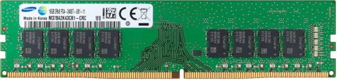
Samsung claims that later this year it intends to use its 1x nm manufacturing technology to make LPDDR memory with increased capacity, which should help makers of smartphones, tablets and notebooks boost the amount of DRAM inside their devices or reduce pricing.
Use of the sub-20 nm process technology to produce 8 Gb DDR4 chips should make such DRAM ICs cheaper (eventually), which will help PC and server makers to install more memory without increasing prices of their products. At press time, one 8 Gb DDR4 chip costs $4.688, according to DRAMeXchange. By contrast, a 4 Gb DDR4 IC is priced at $1.672. Therefore, using low-capacity chips is still cheaper than using high-capacity DRAM devices. Meanwhile, if you are building servers, you might not have a choice but to utilize 8 Gb chips to create high-end memory modules (i.e., with 128 GB capacities). For that reason, for server manufacturers, Samsung’s new 8 Gb DDR4 chips should be useful.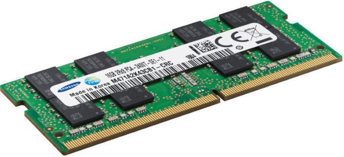
Gallery: Samsung Begins To Produce DDR4 Memory Using 10 nm-Class Process Tech


More...


 Quote
QuoteThread Information
Users Browsing this Thread
There are currently 40 users browsing this thread. (0 members and 40 guests)


Bookmarks