

Results 5,901 to 5,910 of 12094
Thread: Anandtech News
-
04-07-16, 02:40 PM #5901
Anandtech: EVGA Releases GeForce GTX 950 Low Power Graphics Cards with 75W TDP
EVGA this week unveiled their NVIDIA GeForce GTX 950-based video cards with reduced power consumption. As a result, these new cards do not require auxiliary power connectors and can be powered entirely by a PCIe x16 slots Similar variants have already been announced from companies like ASUS and MSI, but EVGA decided to release a range of such graphics cards as well, including factory-overclocked models.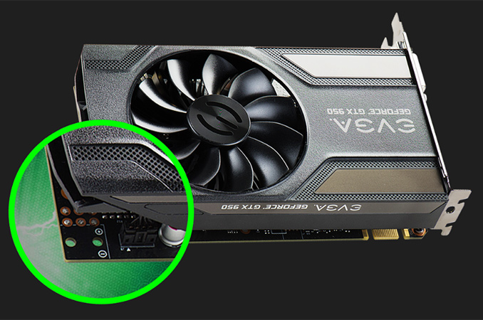
EVGA’s family of low-power GeForce GTX 950 graphics cards that do not need external power consists of four models, which is a lot by contrast to other manufacturers. The GPUs are based on NVIDIA’s cut-down GM206 graphics die (768 stream processors, 48 texture units, 32 ROPs, 128-bit GDDR5 memory interface) but use EVGA’s custom PCB with 3+1 phase VRM. The GPUs are equipped with 2 GB of GDDR5 memory, one or two DVI connectors depending on model, one HDMI 2.0 port and one DisplayPort output.
From the four cards, two of them run at NVIDIA’s reference GPU clock rates of 1025/1190 MHz, while the other two a little bit faster and run the graphics chip at 1076/1253 MHz. In each pair, one has a single DVI-I while the other has DVI-I and DVI-D connectors. All the boards feature 6.6 Gbps GDDR5 memory. As for cooling, they use dual-slot single-fan EVGA ACX 2.0 coolers.
Unfortunately, EVGA does not mark its GeForce GTX 950 boards with reduced power consumption with any easy to recognize label, hence, the only way to distinguish the adapters without PCIe connectors is by referencing the product numbers:
While graphics cards like the GeForce GTX 950 are not used to build high-end gaming PCs, these new PCIe-less models can be purchased to upgrade inexpensive or older PCs which sometimes come without an auxiliary PCIe power connector on the power supply. In addition, a GM206-based adapter is a reasonable choice for an HTPC as the GPU supports hardware-accelerated decoding and encoding of H.265 (HEVC) video, as well as HDCP 2.2 content protection over HDMI 2.0 (which is required for Ultra HD Blu-ray playback).NVIDIA GeForce GTX 950 Graphics Cards Specification Comparison EVGA GTX 950 EVGA GTX 950 EVGA GTX 950 EVGA GTX 950 MSI
GTX 950ASUS
GTX 950Ref Product Name 02G-P4-0952 02G-P4-0956 02G-P4-0954 02G-P5-258 2GD5 OCV2 GTX950-2G - CUDA Cores 768 Texture Units 48 ROPs 32 Core Clock 1025
MHz1076
MHz1025
MHz1076
MHz1076
MHz1026
MHz1024
MHzBoost Clock 1190
MHz1253
MHz1190
MHz1253
MHz1253
MHz1190
MHz1188
MHzMemory Clock 6.6 Gbps
GDDR5Memory Bus Width 128-bit VRAM 2 GB TDP 75 W 90 W Outputs DVI-I
DP 1.2
HDMI 2.0DVI-I
DP 1.2
HDMI 2.0DVI-D
DVI-I
DP 1.2
HDMI 2.0DVI-D
DVI-I
DP 1.2
HDMI 2.0DVI-I
DisplayPort 1.2
HDMI 2.0Architecture Maxwell 2 GPU GM206 Transistor Count 2.94 B Manufacturing Process TSMC 28nm Launch Date Apr '16 Mar '16 Mar '16 Aug '15 Launch Price unknown $159
Since at least three manufacturers of NVIDIA graphics cards already offer GeForce GTX 950 boards without auxiliary PCIe power connectors, it is could be assumed that the GM206-251 GPU (revealed by MSI) has been selected due to reduced power requirements. It is unclear whether NVIDIA picks such GPUs itself and then marks them accordingly, or if there is a new revision of the chip and makers of add-in-cards have to test power requirements themselves through binning.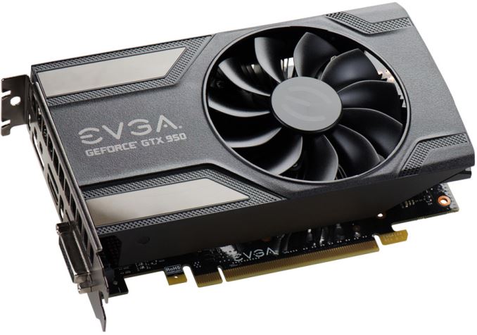
Right now EVGA does not sell its GeForce GTX 950 low power graphics cards on its website. It is unknown at what price these units will be launched at this time.
More...
-
04-08-16, 12:00 AM #5902
Anandtech: Meizu Launches the m3 note
With every year, we tend to see quite a few launches happen in the first two quarters as the cycles in supply chains align for mass production to start around this time. We’ve already seen a number of new products from Huawei, LG, Samsung, and Xiaomi. Meizu is the latest company to join this list with its announcement of the m3 note.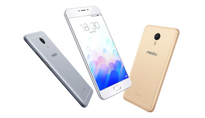
With a 6061 aluminum unibody design, the m3 note draws heavily from the PRO 5. The rear camera is accentuated by a large, black surround with the pill-shaped dual-color LED flash sitting just below. Unlike the PRO 5, however, the camera sits flush with the back. Meizu’s unique T-slot design also carries over from the PRO 5. Instead of the usual plastic antenna strips, Meizu machines slots into the aluminum back, whose polished finish provides a nice contrast to the sandblasted aluminum.
The volume rocker switch sits above the power button inside a groove machined into the right edge, while the SIM and SD card combo slot is on the left edge. A 3.5mm headphone jack is found up top. The downward firing speaker sits next to a centered microUSB port on the bottom.
The m3 note’s 5.5-inch FHD IPS display—which reaches a peak brightness of 450 nits, according to Meizu—sits behind edge-to-edge glass. There’s also an mTouch 2.1 fingerprint sensor below the screen that’s surrounded by a stainless steel accent ring. Overall, the rounded corners, beveled edges, and 2.5D curved cover glass give the m3 note a similar in-hand feel to the iPhone 6s Plus.
Inside the aluminum chassis is an octa-core MediaTek Helio P10 SoC. This midrange SoC uses four ARM Cortex-A53 CPUs with a max frequency of 1.8GHz and another four with a max frequency of 1.0GHz in a big.LITTLE arrangement. These frequencies are a little below the P10’s rated frequencies of 2.0GHz and 1.1GHz, respectively. So either Meizu is underclocking the P10 to save power, or it’s using a lower-binned version of the P10.Meizu m3 note Specifications SoC MediaTek Helio P10 (MT6755)
4 x 1.8GHz Cortex A53 (Performance)
4 x 1.0GHz Cortex A53 (Efficiency)
Mali T860MP2RAM 2/3GB LPDDR3-833 NAND 16/32GB (eMMC 5.1) + microSD Display 5.5" 1920x1080 IPS LCD Modem 2G / 3G / 4G LTE Category 6
(Integrated MediaTek WorldMode)
Dual SIM DSDSDimensions 153.8mm x 75.6mm x 8.2mm; 163g Camera Rear Facing
13MP
f/2.2 PDAF Dual LED FlashFront Facing
5MP
f/2.0Battery 4100 mAh (15.79Wh) Launch OS Android 5.1 with Flyme 5.1 UI Connectivity 802.11 a/b/g/n/ac, Bluetooth 4.0
GPS/GNSS, Micro USB 2.0, DLNALaunch Price (CN) 799/999 RMB (125/155 USD) 2GB/3GB
The P10 SoC also includes an ARM Mali-T860MP2 GPU. This is ARM’s current midrange GPU, which features two ALUs per core instead of three ALUs per core like the high-end Mali-T880.
The m3 note comes in two different configurations: 2GB RAM / 16GB internal storage and 3GB RAM / 32GB internal storage. Both versions support microSD cards for storage expansion and feature a rather large 4100 mAh battery, which should provide the m3 note and its lower-clocked P10 SoC with excellent battery life.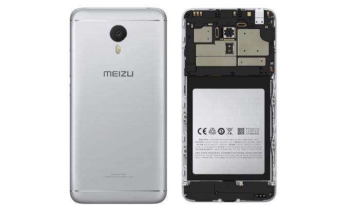
The 13MP rear camera sits behind a 5-piece lens array with an f/2.2 aperture. It’s unclear who makes the sensor, but it does use PDAF to improve focus speed. There’s no OIS support, which is a feature that has yet to trickle down to this price point. The m3 note records video at up to 1080p30, a limit imposed by the P10 SoC.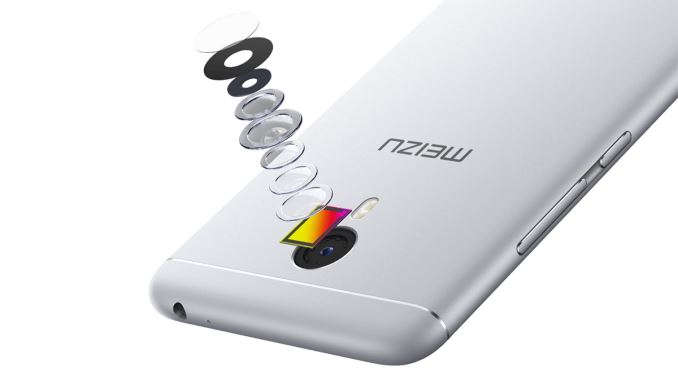
The m3 note comes in three different colors: gold/white, silver/white, and gray/black. It will be available in China for 799 and 999 RMB for the 2GB and 3GB models respectively.
More...
-
04-08-16, 08:02 AM #5903
Anandtech: The SilverStone Strider Platinum 550W PSU Review
Today we are having a look at the “world’s smallest” 80Plus Platinum certified 550W ATX PSU, the SilverStone Strider Platinum. The company boasts that this fully modular, compact PSU is of exceptional quality and can deliver world-class performance, making it ideal for users with constrictive cases.
More...
-
04-11-16, 07:45 AM #5904
Anandtech: SanDisk Extreme 900 USB 3.1 Gen 2 Portable SSD Review
SanDisk launched the Extreme 900 SSD at Computex 2015. The claim to fame was the availability of almost 2TB of flash in a bus-powered enclosure with a USB 3.1 Gen 2 Type-C interface. It was one of the first 2TB-class external drives to arrive in the market. Though the Samsung T3 Portable SSD beat it to our review bench, we finally got SanDisk's review sample last month. Read on for a detailed review of the 1.92TB SanDisk Extreme 900, one of the first USB 3.1 Gen 2 client devices available in the market.
More...
-
04-12-16, 07:17 AM #5905
Anandtech: Hands On With The HTC 10: A Fresh Start
At this point it’s probably not a secret that HTC has been struggling for the past few years. While the One M8 was a solid upgrade to the One M7, it was unfortunate in the sense that it did not resolve the problems that the M7 had. HTC made a leap in extending the One's core strengths of an aluminum unibody design, dual front-facing speakers, and generally polished user experience, but they left other matters unresolved. More frustratingly, with the One M9 it seemed that HTC had taken a step back as there was very little that had meaningfully changed, and it wasn’t entirely unusual to see changes that were a regression relative to the One M8. To be honest, I was ready to write off HTC entirely from the market as the One M9+ felt like it was just more of the same mistakes from HTC.
To see if the HTC 10 is more of the same, read on for the full article.
More...
-
04-12-16, 09:06 AM #5906
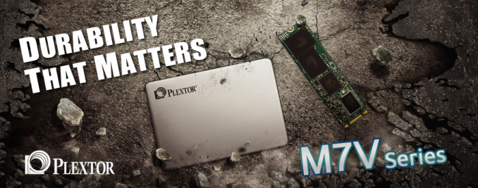
Anandtech: Plextor Embraces TLC NAND: Introduces M7V SSD
After toying with the concept last year, Plextor has finally announced its first family of SSDs based on TLC NAND flash memory. The new M7V lineup of drives is projected to be more affordable than Plextor’s SSDs based on MLC NAND, but the company claims that lower prices will not affect reliability and consistent performance that its SSDs are known for. In fact, Plextor says that its M7V will be better than all the competing TLC-based solutions, which is a a very bold claim indeed.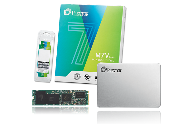
Plextor demonstrated its first TLC-powered drive back at CES 2015. At the time, the SSD was based on the Marvell 88SS1074 controller with LDPC (low-density parity check) error correction for increased endurance as well as Toshiba’s TLC NAND made using its second-generation 19 nm process technology (A19 nm). As it appears, that drive was not the only low-cost option considered by Plextor. By the time company needed to ramp up production of its affordable SSD in mid-2015, it decided to postpone the release of its TLC-powered drive. Instead, the company introduced the M6V, which features Toshiba’s 15 nm MLC NAND, but is powered by a low-cost quad-channel Silicon Motion's SM2246EN controller. As a result, Plextor managed to release a value SSD, but kept using familiar MLC memory (albeit, with a new controller).
Nonetheless, Plextor knew it could not to skip planar TLC NAND (and use 3D NAND once it becomes available instead), which is why it continued to work on its TLC drives. This month, the company finally revealed its first TLC-based product — the M7V.
Marvell’s 88SS1074 Gets a New Version
The Plextor M7V SSDs are based on the Marvell 88SS1074B1 controller as well as Toshiba’s TLC flash memory made using its 15 nm process technology. When Marvell originally introduced its 88SS1074 controller in May, 2014, it emphasized that the chip was specifically designed to enable SSD makers to use TLC NAND, which is why it features its own NANDEdge error correction technology based on LDPC algorithms. Plextor has been working on products featuring this controller for a long time and the M7V is the fruit of this work.
For some reason, Plextor calls the 88SS1074B1 “the next-generation controller”, even though it looks like a new version of the chip introduced two years ago. This is not a bad thing in general because the 88SS1074 is a fine 8-channel NAND controller and Plextor’s engineers should be familiar with it (after a couple of years of playing with it). If the B1 version has higher clock-rates and/or more processing cores, it can perform more error correction and other operations, which potentially can improve endurance, reliability and/or performance of SSDs. In fact, the new revision of the chip could be the key to many technologies Plextor incorporated into the M7V.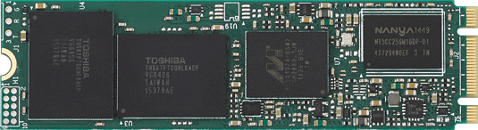
By The Numbers
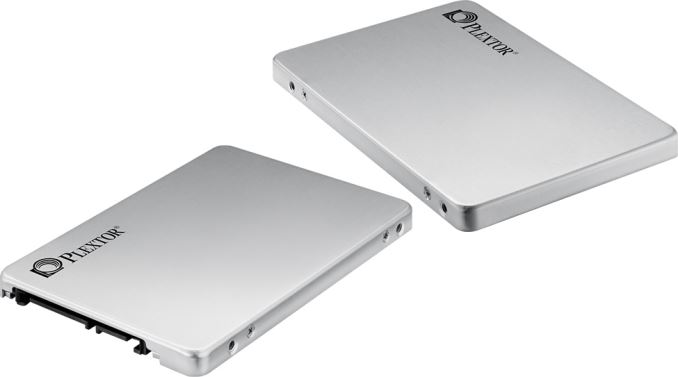
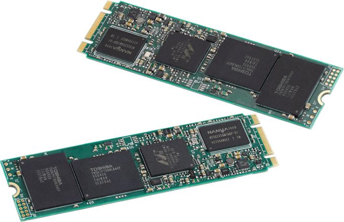
Plextor will offer its M7V family of SSDs in 2.5”/7mm (PX-M7VC) and M.2 2280 (PX-M7VG) form-factors. In the case of the latter, this is a SATA M.2 drive, as the Marvell 88SS1074B1 controller only supports SATA.
Plextor will offer M7V in 128 GB, 256 GB and 512 GB configurations. The drives also come with enlarged DRAM buffers, which are important for performance and, possibly, for Plextor’s way of handling TLC memory.
Plextor claims that maximum sequential read speed of an M7V SSD is 560 MB/s, whereas its maximum sequential read speed is 530 MB/s. Maximum random 4K read/write speed declared by the manufacturer is 98000/84000 IOPS.
It is interesting to note that Plextor’s M7V SSDs are rated faster than the company’s M6V drives both in terms of sequential read/write operations (keep in mind that we are dealing with TLC-based storage devices, hence, we’ll talk about their writing performance below) as well as random read/write operations. Therefore, despite of getting a drive with cheaper memory, owners of the M7V may get higher performance if Plextor's performance numbers prove true.Plextor M7V and M6V SSD Specifications Size 128 GB 256 GB 512 GB 128 GB 256 GB 512 GB Controller Marvell 88SS1074B1 Silicon Motion SM2246EN NAND Toshiba 15 nm Toggle TLC Toshiba 15nm Toggle MLC DRAM Cache 256 MB 512 MB 1GB 128 MB 256 MB 512 MB Sequential Read 560 MB/s 535 MB/s Sequential Write 500 MB/s 530 MB/s 170 MB/s 335 MB/s 455 MB/s 4kB Random Read 97K IOPS 98K IOPS 81K IOPS 83K IOPS 83K IOPS 4kB Random Write 51K IOPS 84K IOPS 42K IOPS 80K IOPS 80K IOPS Warranty 3 years
Gallery: Plextor Embraces TLC NAND: Introduces M7V SSD


Enhanced Endurance & PlexNitro
Plextor claims that it uses TLC NAND memory from Toshiba with increased endurance (which it calls “top-class components”). It also says that its exclusive firmware along with flash components help to increase maximum amount of memory’s P/E cycles to 2000, which is higher compared to that of typical TLC NAND. In fact, durability is what Plextor sees as the main selling point of the M7V.
The company does not specify whether it uses Toshiba’s new TLC NAND devices that architecturally have higher endurance (an unlikely scenario), or Marvell’s 88SS1074B1 controller with LDPC-based error correction technology. Similarly, they aren't saying much about their own firmware, with its own set of tricks. For competitive reasons, Plextor does not specify the amount of NAND used for over-provisioning to increase endurance of its drives (but not components themselves), but extra NAND helps to increase durability of SSDs.
To speed up writing performance of TLC NAND-based SSDs, like most other TLC drive vendors Plextor is employing a write acceleration technology of some kind to speed up write operations, which it calls PlexNitro. The standard here for TLC drives is to implement a pseudo-SLC mode write cache, however it's not clear if this is what Plextor is doing. The uncertainty comes from the fact that Plextor isn't setting aside space for the pSLC cache like other TLC drives have, and is why the M7V ships at 128/256/512GB rather than 120/240/480GB. Whether this means that they're instead dipping into the traditional and innate ~7% spare area pool or something else entirely remains to be seen.
The actual peculiarities of PlexNitro are yet to be discovered, but what Plextor promises - consistently high performance, increased capacities and high endurance - sounds impressive. Still, it's something we'll have to validate once we're able to benchmark the drive and dive deeper into the workings of PlexNitro.
Finally, the new Plextor M7V solid-state storage devices should hit the market later this month. Plextor did not specify recommended prices of its M7V SSDs, but it is logical to expect them to cost less than the company’s MLC-based M6S Plus drives introduced several weeks ago. The Plextor M7V SSDs offer MTBF of up to 1.5 million hours and are covered with a limited three-year warranty.
More...
-
04-12-16, 10:59 AM #5907
Anandtech: Micron Announces 9100 & 7100 Series PCIe Enterprise SSDs
Micron entered the PCIe SSD market in 2011 with the formidable P320h. Using generously overprovisioned 34nm SLC NAND and a controller with 32 NAND channels and a PCIe 2.0 x8 link, the P320h boasted extreme write endurance ratings and performance that is still respectable by today's standards, but with a commensurate price tag. Two years later Micron introduced the P420m with the same controller but 25nm MLC NAND, adding power loss protection capacitors and offering similar performance on read-heavy workloads at a much more accessible price. Today Micron is announcing two new product lines that bring support for NVMe and PCIe 3.0 and use Micron's latest 16nm MLC NAND.
The new Micron 9100 NVMe PCIe SSD series is the high-performance and high-capacity product. Capacity ranges from 800GB to 3.2TB in either half-height half-length add-in card form factor or as a 15mm thick 2.5" U.2 drive. With a TDP of up to 27W, the Micron 9100 SSD is the more direct successor to the P420m and is using a PMC-Sierra controller that is descended from the controller used in Micron's previous PCIe SSDs.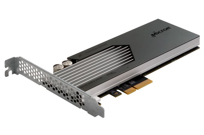
Micron 9100 PCIe SSD Specifications Capacity 800GB 1.2TB 1.6TB 2.4TB 3.2TB Interface PCIe 3.0 x4 HHHL or U.2 Sequential Read 2.1 GB/s 2.8 GB/s 2.8 GB/s 3.0 GB/s 3.0 GB/s Sequential Write 650 MB/s 1.3 GB/s 1.3 GB/s 2.0 GB/s 2.0 GB/s Random Read IOPS 540k 700k 700k 750k 750k Random Write IOPS 55k 180k 100k 300k 160k Idle Power Consumption 7W Active Power Consumption 16W 21W 21W 27W 27W The Micron 7100 NVMe PCIe SSD expands Micron's offerings into a more mainstream segment of the market by adopting Marvell's 88SS1093 controller that is designed for client and smaller enterprise drives. Capacities for the 7100 range from 400GB to 960GB for the M.2 version and from 400GB to 1.9TB as a 7.5mm thick 2.5" U.2 drive. The smaller Marvell controller will keep power consumption below 12.5W and the M.2 version further throttles to a limit of 8.25W.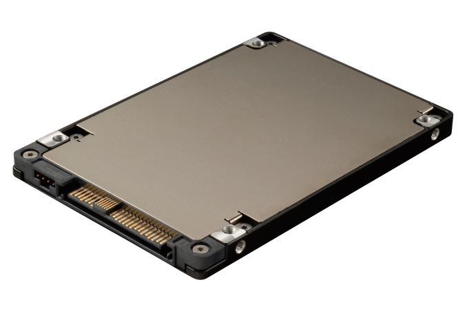
Both the 9100 and 7100 series include models in two tiers of overprovisioning: for read-heavy or mixed workloads. The drives with greater overprivisioning sacrifice some capacity for greatly increased random write speeds and improved write endurance, though specifications for the latter have not yet been released.Micron 7100 PCIe SSD Specifications Capacity 400GB 480GB 800GB 960GB 1.6TB 1.92TB Interface M.2 22110 or 2.5" U.2 2.5" U.2 Sequential Read 2.4 GB/s 2.5 GB/s 2.5 GB/s Sequential Write 475 MB/s (M.2)
500 MB/s (U.2)600 MB/s (M.2)
900 MB/s (U.2)900 MB/s Random Read IOPS 180k 220k 235k Random Write IOPS 25k 10k 33k 12k 40k 15k Idle Power Consumption 3.7W Maximum Power Consumption 8.25W (M.2)
12.5W (U.2)12.5W
More...
-
04-12-16, 01:06 PM #5908
Anandtech: Several CAPI-Enabled Accelerators for OpenPOWER Servers Revealed
Over a dozen special-purpose accelerators compatible with next-generation OpenPOWER servers that feature the Coherent Accelerator Processor Interface (CAPI) were revealed at the OpenPOWER Summit last week. These accelerators aim to help encourage the use of OpenPOWER based machines for technical and high-performance computing. Most of the accelerators are based on Xilinx high-performance FPGAs, but some feature custom silicon.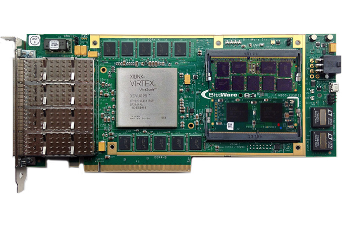
IBM’s CAPI port is a PCIe 3.0-based interconnection specifically designed for programmable processors (e.g., ASICs, GPUs, FPGAs, etc.) that enables them to address the same memory address space as the CPU. CAPI requires custom hardware incorporated into IBM’s POWER8 processors, which is called the coherent accelerator processor proxy (CAPP), as well as a POWER service layer (PSL) integrated into CAPI-supporting processors. CAPP maintains a directory of cache lines held by the accelerator and snoops the processor bus for the accelerator. The PSL performs address translations and holds the coherent data for quick access by the accelerating hardware. To work, CAPI has to be supported by the hardware, the operating system and the application in use. At present, IBM’s POWER8 CPUs, a number of accelerators, RedHat Enterprise Linux 7.2 LE (and higher), and Ubuntu LE, as well as select programs, support CAPI.
IBM and the OpenPOWER Foundation need CAPI in order to enable a relatively simple and inexpensive way to build special-purpose accelerators for various workloads. The aim is to make POWER8-based machines viable for a variety of market segments as well as to create platforms that can process modern workloads faster.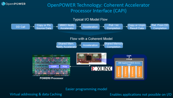
While it is possible to enable unified memory for CPUs and co-processors using custom hardware and multiple tweaks in device drivers, this requires huge investments in silicon development, complex drivers and a number of other things. By contrast, programming an FPGA (field-programmable gate array) is considerably cheaper, and the CAPI technology brings them key heterogeneous processing capabilities. While this does not necessarily enable higher bandwidth between the CPU and the accelerator (after all, CAPI is layered on top of PCI Express 3.0 and a specified peak bandwidth), according to IBM they remove overheads, improve performance and can potentially simplify the workflow for programmers. In short, CAPI is an important part of IBM’s POWER strategy in general as well as OpenPOWER initiative.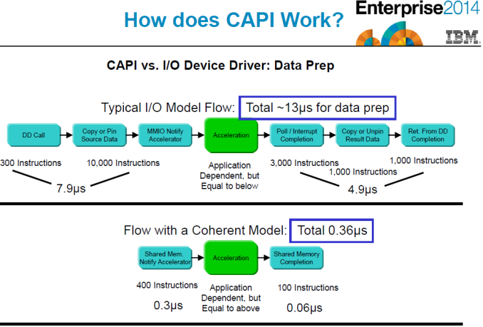
At this year’s OpenPOWER Summit, IBM and its partners revealed over a dozen of special-purpose CAPI-enabled FPGA-based accelerators. This shows that the OpenPOWER platform is gaining interest and investment from different sources. The list of developers includes such companies as BittWare, DRC, IBM, Mellanox, Xilinx and others, but some decided not to publish details about their accelerators, as it seems from OpenPOWER’s press release. The accelerators revealed at the conference are either available or are set to become available in the coming quarters. The devices come in the form of PCIe 3.0 x8 or x16 cards and are compatible with IBM POWER8-based servers. Some are also compatible with machines running other processors (and in this case, CAPI is not supported).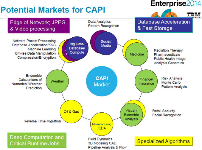
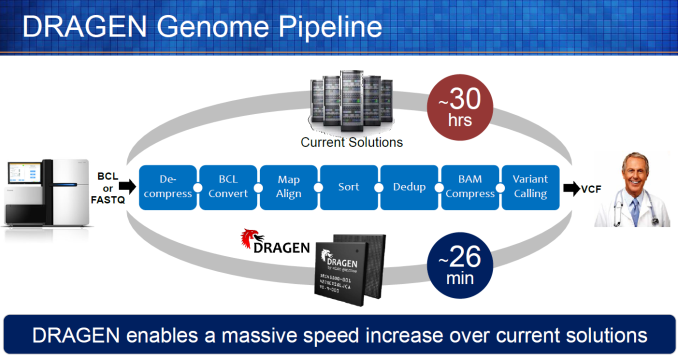
One of the important announcements at the summit was Edico Genome’s DRAGEN genomics platform, which uses an accelerator powered by the Xilinx Virtex-7 980T FPGA and is equipped with 16 GB of quad-channel DDR3L-1866 memory. The platform, which is based on a 2-way IBM S822LC server, can analyze an entire genome in 26 minutes, down from approximately 30 hours on general-purpose processors. An earlier prototype was shown at SuperComputing 2015, however this seems to be the announcement of the full product.IBM CAPI-Compatible Accelerators Developer Model Hardware and Application Alpha Data ADM-PCIE-8K5 Xilinx UltraSCALE KU115-2 FPGA
2×8 GB of DDR4-2400 with ECC (32 GB version can be built)
Dual Firefly connectors for up to 4×16Gbps per connector
Reconfigurable accelerator for custom video processing, machine learning, HPC and network acceleration applications.
Available as add-in PCIe 3.0 x8 cards.BittWare XUSP3S Xilinx Virtex UltraScale 80/95/125/160/190 or Kintex UltraScale 115
2×16 GB DDR4 ECC (64 GB version can be built), QDR memory
Four QSFP28 cages for 1×400GbE, 4×100GbE, 4×40GbE, 16×25GbE, or 16×10GbE
Massive data flow and packet processing.
Available as add-in PCIe 3.0 x16 cards.DRC GraphFind Xilinx Kintex UltraScale KU115 FPGA
Can rapidly discover relationships between people, places, events, and objects. Simultaneously identifying focal points with weighted strengths of connections.
Available as a PCIe card, or as a pre-configured appliance consisting of multiple cards.DRC Novara Xilinx FPGA
A search engine and an accelerator, which identifies key imprecise phrases and Bit patterns using a fuzzy logic analyzer that can instantly analyze millions of messages and data streams without the need to index first. Can process up to 2.5 GB of data per second.
Available as 1U server, which contains up to four Novara cards. Servers can be clustered.DRC Ferrara2 Xilinx FPGA, four QSFP28 cages.
Encrypts and/or authenticates data using AES-256 algorithm with bit-splitting capability from Security First Corporation (SFC) at line rates up to 40 Gb/s.
Available as PCIe 3.0 x16 add-in boards for servers, communication or storage systems. Multiple Ferrara2 boards can be placed in one system.Edico Genome DRAGEN Genomics Platform Xilinx Virtex-7 980T FPGA
4×4 GB DDR3L-1866 memory.
Analyzes an entire human genome in 26 minutes (vs. 30 hours on general-purpose hardware). Enables healthcare providers to identify patients at higher risk for cancer before the conditions worsen.
Compatible with the IBM S822LC server. Available in a pre-configured Power8 server.IBM Prototype Xilinx Virtex UltraScale 190
16 GB of Micron HMC memory.
Acceleration of in-memory computing applications.
Available as add-in PCIe 3.0 x16 cards.IBM,
Nallatech,
RedisLabs
AlteraIBM Data Engine for NoSQL IBM Power S822L server(s)
IBM FlashSystem 840 or 900 all-Flash storage system(s)
Altera Stratix V FPGA-based interconnection card with 10 GbE SFP+ ports by Nallatech
IBM FlashSystems are attached to the POWER8 processor through the CAPI coherent attach card.
Thanks to the new interconnection method, the Redis Enterprise Cluster application can issue read/write commands that eliminate 97% of the code path length.
According to IBM, this enables IBM Data Engine for NoSQL to access Flash within latency levels comparable to traditional RAM-based x86 implementations.
Various configurations available.IBM, Nallatech, Samsung, Xilinx Prototype Xilinx FPGA
2×1 TB Samsung M.2 NVMe SSDs.
IBM Data Engine for NoSQL, which allows fast application exploitation in a smaller, in-server form-factor.
Available as add-in PCIe 3.0 x8 cards.Mellanox ConnectX-4 VPI ConnectX-4 VPI
ConnectX-4 adapter cards with virtual protocol interconnect (VPI) support EDR 100 Gb/s InfiniBand and 100 Gb/s Ethernet connectivity.
Available as add-in PCIe 3.0 x16 cards.Semptian NSA-120
NSA-120BXilinx Kintex UltraScale XCKU060/XVKU115
2×4 GB or 2×8 GB DDR3-1600 memory with ECC
Two SATA interfaces
Network and service accelerator. Can be used in big data analysis, image recognition/processing, video encoding/decoding, data compression/decompression, data encryption/decryption, voice recognition, neural network, machine learning, network security, etc.
Available as add-in PCIe 3.0 x8 cards.
Other interesting solutions discussed at the summit include an FPGA-based accelerator for discovering relationships hidden in big data; an FPGA-powered fuzzy search engine for imprecise string searching and matching, which can analyze millions of messages and data streams without indexing; as well as various reconfigurable accelerators for HPC, Big Data, and so on. IBM also mentions that there are companies offering CAPI-enabled building blocks for FPGAs for computer vision, machine learning, and other applications. Some of those companies are startups or working in stealth mode (we do not know whether they developed their building blocks thanks to the SuperVessel program, though this is a possibility), and they may announce their products over time.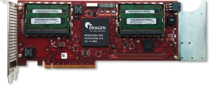
While the number of CAPI-enabled accelerators available today is not high, it is growing, which is a good news for the OpenPOWER ecosystem. Positive news (from IBM) is the number of China-based companies developing accelerators featuring CAPI, which shows that local companies in growing markets for servers are expressing interest in such solutions.
More...
-
04-12-16, 08:36 PM #5909
Anandtech: Micron Presents New SSDs and Strategy
At Micron's Enterprising event today in Austin, TX the company discussed several upcoming products and shared information about an ongoing strategic shift. Not content to stay a mere component supplier for storage and memory, Micron is getting involved in software to help develop solutions that can make the most of their storage hardware offerings. The venue was Micron's new Storage Solutions Center, the nexus of Micron's collaboration efforts with OEMs, software vendors and enterprise end-users. At the Storage Solutions Center, Micron and their partners work on whole-system optimization to solve immediate customer needs and to generate reference architectures and documentation for the benefit of other customers.
The reference architectures are branded as Micron Accelerated Solutions, the first of which is a hardware platform by Supermicro bundled with VMWare Virtual SAN and using Micron M510DC SSDs. A similar solution has been developed with the Ceph object storage system and work is underway with Nexenta on an integrated system that will be available in the second half of the year.
In addition to the whole-system products, Micron shared information about several new and upcoming SSDs. The 9100 and 7100 series PCIe SSDs were launched and covered in a separate post. The 9100 was featured in a demo of the software defined storage system under development by SymbolicIO. The 7100 series is the second product line resulting from Micron's collaboration with Seagate, which previously resulted in a family of SAS SSDs.
Micron announced the schedule for their first 3D NAND SSDs. The Crucial MX300 will launch later this month using Micron's 3D TLC NAND. Specifics aren't available yet, but given the 384Gbit (48GB) capacity per die of the 3D TLC, the MX300 will either feature oddball capacities, significantly more overprovisioning than its MLC-based predecessors, or an uneven distribution of NAND dies across the controller's channels.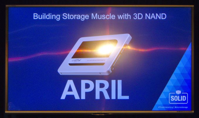
In June Micron will launch a pair of OEM client SSDs, the 1100 series and the 2100 series. Specifications for those drives were also not announced, but the photographs reveal some details: an M.2 SATA drive using a Marvell controller (probably 88SS1074, and thus probably also using TLC), and an M.2 PCIe drive with a Silicon Motion controller, presumably the SM2260.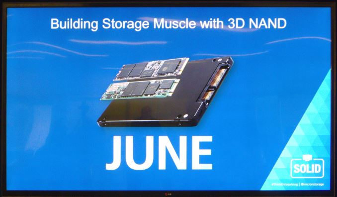
Micron says there will be 3D NAND for the datacenter in the second half of the year, but they have not yet identified any of the drives that will be using it. A 3D XPoint wafer was waved around onstage but Micron made no substantial announcements today about the technology. They did promise that we'll be hearing more about the products and their branding later this year, and confirmed that they've been focusing on using 3D XPoint in NVMe products (whereas Intel is also developing NVDIMMs).
More...
-
04-13-16, 05:26 AM #5910
Anandtech: Meizu Announces New PRO 6
Today Meizu launches the new PRO 6. The company had launched the PRO 5 only last September so this is a significant change in the release-schedule of the PRO series as we see the new unit come a mere 7 months after its predecessor. The "Pro" series initially debuted with the MX4Pro which we reviewed last year, since then Meizu has dropped the MX name to better differentiate between the "premium" PRO models and the more mainstream MX lineup. The PRO 6 in some ways continues where the PRO 5 left off, but at the same time makes some larger changes in terms of form-factor and component choices.
The PRO 6 is quite a strange successor as at first glance the upgrades aren't quite evident. The PRO 6 replaces the traditional Samsung LSI Exynos SoCs with MediaTek's Helio X25. The X25 is exclusive to the PRO 6 and essentially is an X20 with the dual-core A72 cluster clocked in at 2.5GHz instead of 2.3GHz. The three-cluster design also features a quad-core A53 at 2.0GHz as well as a low-power A53 quad-core at 1.4GHz. On the GPU side we see a Mali T880MP4 at 700MHz. Main memory is 4GB of LPDDR3 running at 933MHz.Meizu PRO Series Specifications Meizu PRO 6 Meizu PRO 5 SoC MediaTek Helio X25
2x A72 @ 2.5GHz
4x A53 @ 2.0GHz
4x A53 @ 1.4GHz
Mali T880MP4 @ 700MHzSamsung Exynos 7420
4x A57 @ 2.1GHz
4x A53 @ 1.5GHz
Mali T760MP8 @ 770MHzRAM 4GB LPDDR3-1866 3 / 4GB LPDDR4-3200 NAND 32 / 64GB eMMC 5.1 NAND 32 / 64GB UFS 2.0
+ microSDDisplay 5.2” 1080p AMOLED 5.7” 1080p AMOLED Modem 2G/3G/4G LTE Cat 6
(Integrated MediaTek SoC Modem)2G/3G/4G LTE Cat 6 Dimensions 147.7 (h) x 70.8 (w) x 7.25 (d) mm
160g156.7 (h) x 78 (w) x 7.5 (d) mm
168gCamera Rear Camera
21.16MP ( 5444 x 4016 )
Sony IMX230 1/2.4" 1.12µm pixels
F/2.2 aperture
w/ Laser & Phase Detection focusRear Camera
21.16MP ( 5444 x 4016 )
Sony IMX230 1/2.4" 1.12µm pixels
F/2.0 aperture
w/ Laser & Phase Detection focus
w/ Dedicated Samsung ISPFront Facing Camera
5MP 1.4µm pixels
F/2.0 apertureFront Facing Camera
5MP 1.4µm pixels
F/2.0 apertureBattery 2560mAh (~9.85 Whr) 3050mAh (~11.74 Whr) Launch OS Android 6.0 with FlyMe 5.6 Android 5.1 with FlyMe 5.0 Connectivity 802.11a/b/g/n dual-band 2.4 & 5GHz
BT 4.1, GPS/GNSS, NFC
USB-C 3.1802.11 b/g/n/ac
BT 4.1 + BLE, GPS/GNSS
USB-CSIM Size NanoSIM + NanoSIM NanoSIM Launch MSRP 32GB
RMB ¥2499
(USD~386, ~340€, ~271£)3GB/32GB
RMB ¥2799
(USD~438, ~393€)64GB
RMB ¥2799
(USD~432, ~381€, ~304£)4GB/64GB
RMB ¥3099
(USD~485, ~435€)
The SoC choice puts the PRO 6 in a weird position when compared to the PRO 5 as except for single-thread performance the X25 should theoretically represent a downgrade compared to the Exynos 7420 in last year's model. It's especially in terms of power efficiency where this raises question as we move from a 14nm FinFET design back to a 20nm planar manufacturing process, so I hope that Meizu's SoC choice doesn't negatively impact power efficiency of the phone.
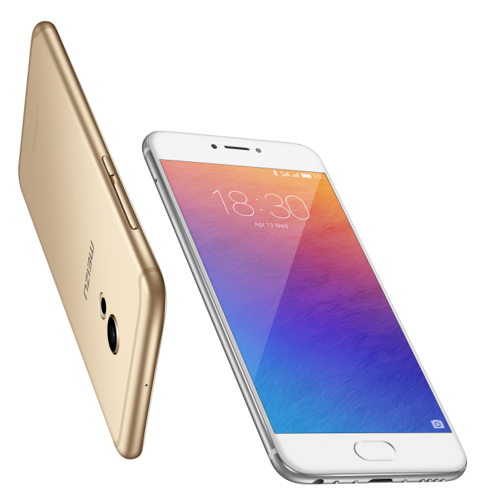
In terms of design the PRO 6 doesn't differ too much from the PRO 5, that is until one takes into account the form-factor of the new model. On the front we see very little distiguishable differences - except for the fact that Meizu downgraded the screen size from 5.7" down to 5.2" marking a departure from the larger "phablet" size. The display panel remains a 1080p AMOLED sourced by Samsung Display.
A first for Meizu is now the inclusion of a pressure sensitive touchscreen module which Meizu calls 3D Press. As we've seen in Apple's latest iPhones or even Huawei's implementation on the Mate S, this is a hardware feature that will undoubtedly depend on the software framework and applications to expose and take advantage of the new functionality. Meizu here might have some better lee-way in terms of Android customization when compared to other vendors who have to adhere to Google's CTS requirements, so it will be interesting to see what Meizu was able to come up with in the latest FlyMe 5.6 OS.
The reduction in size also has an impact on the integrated battery's capacity as we move from a 3050mAh cell down to a 2560mAh unit. Oddly enough, the device only loses 8g and remains relatively heavy for a 5.2" device, coming at 160g.
The main camera remains unchanged from the PRO 5, we find the same 21.16MP Sony IMX230 module featuring both PDAF as well as Laser auto-focus. We see a downgrade in the optics as the PRO 6 features an aperture of F/2.2 compared to the PRO 5's F/2.0 lens. The front-facing camera remains a 5MP unit with 1.4µm pixels.
The PRO 6 comes in 32GB or 64GB models RMB ¥2499 (USD~386, ~340€, ~271£) and RMB ¥2799
(USD~432, ~381€, ~304£) with pre-orders starting now.
More...


 Quote
QuoteThread Information
Users Browsing this Thread
There are currently 18 users browsing this thread. (0 members and 18 guests)


Bookmarks