

Results 6,031 to 6,040 of 12091
Thread: Anandtech News
-
05-31-16, 09:06 AM #6031
Anandtech: HSA 1.1 Specification Launched: Extending HSA to More Vendors & Processor
For the last few years now we have been keeping tabs on the development of the Heterogeneous System Architecture, a set of technical standards and an associated instruction language designed to allow efficient heterogeneous compute. Originally envisioned by AMD, HSA has been the cornerstone of their efforts to develop a fully functional ecosystem for heterogeneous hardware and software. Define a standard, make it easy(ier) for developers to create software around it, and, if all goes well, AMD’s big bet on GPU technology made almost 10 years ago will pay off.
However while AMD was the birthplace of what would become HSA, the standard as a whole has been about more than just one company. Which is why HSA has been under development of the HSA Foundation since 2012. The foundation is composed of many members, including a number of CPU/GPU design heavyweights such as ARM, Qualcomm, Imagination, and Samsung, all of whom are contributing to the development of HSA, and in turn we expect are at least giving themselves the option to leverage it in the future.
With all of that said, while HSA itself is a group project, in practice the first iteration of the standard was AMD-focused. This owed to not only AMD’s early involvement, but also due to the fact that the standard needed hardware to be developed against – to have a proof of concept, which was AMD’s Carrizo APU. As a result the HSA 1.0 specification did not offer as much flexibility with other architectures as the rest of the foundation would like. This is something that they have been working behind the scenes to address, and today the Foundation will finally be taking their next step with the publication of the HSA 1.1 standard.
The big (though not sole) focus of the 1.1 standard then is extending it to better work with non-AMD hardware. This includes not only SoCs and other integrated devices from other vendors (e.g. ARM), but additional classes of accelerators such as DSPs. The HSA foundation wants to make the HSA standard truly heterogeneous for more than just AMD APUs, and for more than just CPU + GPU combinations. The 1.1 standard, in turn, is their effort to form a more perfect standard for heterogeneous compute.
What’ on the table for HSA 1.1 then is not a radical departure from HSA 1.0, but it is an extension and a further tightening of the standard to meet the goals of the Foundation. On the hardware side this is fully backwards compatible – meaning it will work on 1.0 hardware such as Carrizo – while setting up the updated standard to work on additional hardware. This is especially the case with additional classes of accelerators, as 1.0 was primarily focused on abstracting away the GPU (per AMD’s APU needs).
As the first version of the true multi-vendor specification then, 1.1 is designed to help vendors be able to mix and match HSA-capable blocks in an effective manner. The Foundation itself has a heavy mobile SoC presence (be it integrators or IP providers), and it’s easy to imagine how someone like MediaTek would want to be able to ensure that they can easily make HSA-capable SoCs using both Imagination and ARM GPUs, or how Qualcomm may want to use HSA in the future in their Hexagon DSPs. To get there, the 1.1 specification makes transparent a number of system level issues. Information about shared page tables, signals, queues, and more are now better exposed through the updated standard, which plays a big part in bringing about multi-vendor support.
The 1.1 specification also addresses some other issues that were felt at one point or another with HSA. The memory model now has a formal definition (using cat/HERD, for those few of you who know those tools). Along those lines there is additional memory functionality such as support for non-temporal memory accesses, which specifically comes into play when you need to tell the cache to flush an item after it’s used (good for one-time-use items). And on the signal side of matters, HAS code can now understand how to wait on multiple signals, an improvement over 1.0 where code could only wait on a single device.
Finally, 1.1 also includes updates to help optimize performance and make the API play nicer with other code. A new profiling API has been introduced, which exposes hardware-level counters and other information to allow better profiling of the performance of HSA program execution, which can then be fed back into profile guided optimizations. Meanwhile the HSA finalizer has been reworked so that its internal representation isn’t quite so obscure, with the new, more standard-looking representation making the finalizer more suitable for linking to other tools.
Yet despite all of these updates, the change should be completely transparent to application developers. Because HSA is ultimately a means of abstracting away the work and the quirks necessary to make heterogeneous compute work well, application developers won’t see these changes. Who does see these changes are the hardware developers, who write the associated runtimes that actually compile HSAIL intermediate code down to device code. And even then, we’re told that updating a 1.0 implementation to 1.1 is not especially painful, particularly when compared to writing an implementation to begin with. AMD for their part already has a 1.1 implementation up and running, which, logically enough, is being used as the basis of their Radeon Open Compute Platform (ROCm), where ROCm adds the additional discrete GPU functionality AMD specifically needs.
Though with that said, the existence of ROCm and other platforms does bring up the struggle the HSA Foundation is facing on adoption. While ROCm is HSA-based, at the same time AMD is doing an end-run around the HSAIL, preferring to compile direct-to-ISA. This still utilizes the HSA Runtime, and as a result benefits from and validates the basic HSA strategy, but it’s an example of how the HSAIL aspect of the standard has struggled. Earlier this week we saw ARM pass on embracing HSAIL as well for the heterogonous aspects of their Mali-G71 GPU.
ARM for their part is following an OpenCL-centric strategy for exposing the heterogeneous aspects of their hardware to developers. The interesting thing about the ARM implementation is that they have gone above and beyond the basic aspects of OpenCL 2.0, offering finer-grained sync that OpenCL requires at a minimum. Finer-grained sync that would otherwise be something better suited for HSA. As a result part of the HSA Foundation’s efforts are focused on showcasing the additional benefits of HSA over OpenCL 2.0, to entice hardware manufacturers and developers into using HSA.
Ultimately, in our discussion with Foundation president John Glossner (who replaced Phil Rogers), despite these setbacks he’s still bullish on HSAIL. It’s his hope that as finalizers continue to improve, there will be less reason for companies like AMD to bypass HSAIL as they do now. And in the meantime, further success with HSA and HSAIL in general should help to encourage more hardware vendors to adopt HSAIL.
Finally, to pull one more slide out of the HSA deck as a “this is cool” subject, Continuum Analytics’ Numba Python compiler has recently added direct HSA support. This makes it a lot easier for developers writing code in Python to easily add HSA-compliant vectorization to their programs. Python is a widely used language, and while even “automatic” parallelization isn’t the true holy grail of no-effort program parallelization, it does get HSA one step closer, at least in this case.
Wrapping things up, today’s launch of the HSA 1.1 specification, despite the minor version number increment, should in the long run prove to be a significant event for the HSA Foundation. By finally getting the specification to the point where it can more readily support multi-vendor hardware, the ecosystem as a whole will have the opportunity to evolve into a true multi-vendor ecosystem, the ultimate purpose of AMD spinning their work off into the HSA Foundation to begin with. The hard part as an outside observer will be waiting; while the specification was ratified back in April, there is still going to be some lag between the ratification and when additional hardware will be ready to support it.
More...
-
05-31-16, 10:30 AM #6032
Anandtech: Micron Launches 3D NAND Client SSDs
Today Micron is announcing their first client/OEM SSDs with 3D NAND. First mentioned at an enterprise announcement event in April, the Micron 1100 and 2100 SSDs are part of an aggressive transition strategy that has switched almost all of their flash production capacity over to 3D NAND and left only enough 16nm output to fulfill their obligations for existing product lines.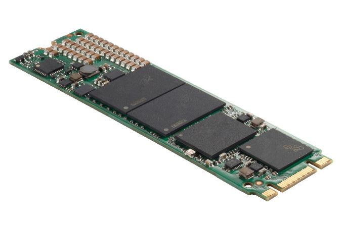
The Micron 1100 is a mainstream client SATA drive in M.2 and 2.5" form factors. It uses Marvell's 88SS1074 controller and Micron's 384Gb 32-layer TLC NAND and is the replacement for the Micron M600, which used their 16nm MLC. Micron's 3D TLC is unusual in having a capacity (48GB) that is not a power of two, but the 1100 retains the traditional drive capacity points of 256GB, 512GB and 1TB, and extends the line to 2TB. Micron hasn't yet disclosed how many dies and how much overprovisioning each model will have, but the 256GB model will probably include 6 dies giving a raw capacity of 288 GiB.
The Micron 1100 has slightly reduced performance and endurance specifications relative to the M600, but it retains the full feature set including TCG Opal encryption, partial power loss protection and SLC caching. The Marvell 88SS1074 was designed with TLC NAND in mind and thus also brings LDPC error correction support.Micron 1100 Specifications Capacity 256GB 512GB 1TB 2TB Controller Marvell 88SS1074 NAND Micron 384Gb 32-layer 3D TLC Form Factors 2.5" 7mm, M.2 2280 single-sided 2.5" 7mm Sequential Read 530MB/s 530MB/s 530MB/s 530MB/s Sequential Write 500MB/s 500MB/s 500MB/s 500MB/s 4KB Random Read 55K IOPS 92K IOPS 92K IOPS 92K IOPS 4KB Random Write 83K IOPS 83K IOPS 83K IOPS 83K IOPS DevSlp Idle Power 2mW 2mW 4mW 25mW Encryption TCG Opal Endurance 120TB 240TB 400TB 400TB
The Micron 2100 M.2 PCIe NVME will be Micron's first client PCIe SSD and their first PCIe SSD with 3D NAND. Micron has not yet finalized the technical specifications for the 2100, but we do know it will be available in capacities up to 1TB as a double-sided M.2 2280 card.
The Micron 1100 will begin mass production in July, followed by the 2100 by the end of summer.
More...
-
05-31-16, 11:13 AM #6033
Anandtech: HP and MSI Demonstrate Backpack PCs for VR Gaming
Virtual reality gaming promises to drive demand for higher-performance graphics cards as well as richer game content. But even before the first AAA VR games make their debut, computer manufacturers are inventing a new PC form-factor specifically for virtual reality gaming: backpack PCs. Truth to be told, the concept of such systems sounds somewhat odd, but HP and MSI think it's worth investigating ahead of any attempts at commercialization.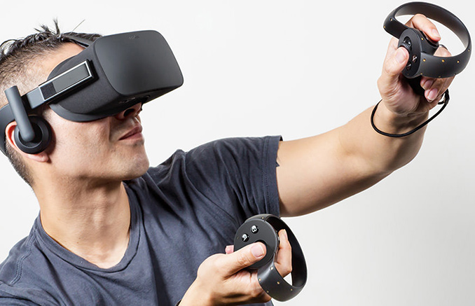
Virtual reality gear changes the way we perceive games, whereas specially designed controllers (e.g., Oculus Touch) are supposed to change the way we interact with video games. Meanwhile, backpack PCs are expected improve the way we feel VR video games by enabling relative freedom of movements by making wiring of the VR headsets a little more comfortable.
Backpack PCs are essentially fully-fledged personal computers without displays, which are integrated into special backpacks, which can then be worn and used to play games. For example, MSI’s Backpack PC contains Intel’s mobile Core i7 Extreme processo as well as NVIDIA’s GeForce GTX 980 graphics adapter along with RAM, SSD, networking capabilities and so on. Meanwhile, HP’s Omen X VR Backpack Concept integrates an Intel Core i5/i7 CPU as well as up to 32 GB of memory (which implies on rather high-end specs in general). The HP backpack PC features only one HDMI output, two USB ports as well as an audio jack (everything one needs to connect the HTC Vive) and a power input. As of now, the Omen X VR Backpack Concept has a battery that only lasts an hour, but allows swapping bats without shutting the PC down. Both systems are compatible with wireless keyboards and mice, so users can navigate typical Windows apps (or rather solve problems with software) with relative convenience.

Because it is not possible to build wireless VR headsets due to latency issues right now, backpack PCs can indeed improve VR experience. However, keep in mind that Oculus Rift’s positional tracking system (the Constellation) connects to PCs using a USB cable, which means that while the backpack PC can enable some additional freedom of movement compared to conventional desktops or laptops, it still needs to connect to the Constellation IR LED sensor for positional tracking. With the HTC Vive everything is a little easier since the tracking system does not need to be connected to the PC itself.

HP plans to supply its Omen X VR Backpack Concept to select software developers in the coming weeks. This will help the company not only to ensure that makers of apps take such PCs into account when they create their programs, but will eventually provide them with valuable input regarding necessary design and features. In addition, the backpack PCs are going to be used in various VR showrooms to demonstrate advantages of virtual reality.
It is unknown if and when backpack PCs will make it to the market, and how much companies like MSI or HP intend to charge for such systems.
Right now, the backpack PCs help game developers to design games, which will be used with wireless VR headsets when and if they emerge. However, it is unclear how comfortable it is to play a game with a PC on your back, albeit, a small one. Therefore, it is difficult to say whether backpack PCs can be commercially successful.
Sources: MSI, Tom’s Guide, The Verge.
More...
-
05-31-16, 01:06 PM #6034
Anandtech: FSP Enters the Market of High-Wattage SFX PSUs with Dagger
FSP has introduced its first power supplies in SFX form-factor designed for high-performance gaming PCs. The new Dagger family of PSUs will contain 500 W and 600 W models that feature a modular design 80 Plus Gold rated. With this latest PSU release, FSP will join a very narrow crowd of PSU makers who build SFX power supplies for gaming PCs.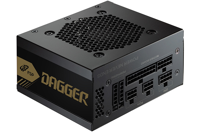
When it comes to high-wattage SFX power supplies for gaming PCs, the users have a choice between only two major brands: Corsair and Silverstone. While these companies are well known and are very respected by the DIY community, the lack of serious competition has its effect on prices, which is why SFX PSUs are rather expensive for their wattage. FSP, the new kid on the block, will become the third major brand to offer SFX power supplies for gaming systems, which is a positive thing for the market.
The FSP Dagger family will initially include two models rated for 500 W and 600 W maximum load. Both PSUs are compliant with SFX12V V3.3 and ATX12V V2.4 specifications as well as carry the 80 Plus Gold certification. Both PSUs will be equipped with an 80 mm dual ball bearing fan and both feature modular design to ensure easy cable management and clean system builds. Finally, FSP claims that its Dagger PSUs sports a special cross-regulation mode to handle unbalanced loads, which are common for some gaming PCs.
The Dagger PSUs will have EPS12V power connectors (one 24-pin and a 4+4-pin connector), will sport two PCIe 6-pin power connectors as well as several SATA power connectors. While it will be possible to use such power supplies for systems featuring high-end graphics cards that only have one 8-pin PCIe or two 6-pin PCIe auxiliary power connectors, the FSP Dagger PSUs will not be able to work with graphics adapters that require two 8-pin PCIe inputs (from formal point of view, of course). For example, NVIDIA’s GeForce GTX 1080 has one 8-pin PCIe auxiliary power connector, which can be plugged to two 6-pin PCIe connectors using a special adapter. Meanwhile, AMD’s Radeon R9 Fury X uses two 8-pin aux PCIe power inputs, which is why it is formally incompatible with the Dagger.FSP Dagger Series Connector type Hardwired Modular ATX 24 Pin - 1 EPS 4+4 Pin - 1 PCI-E 6 Pin - 2 Peripherals - ?
The Dagger power supplies from FSP will hit the market later this year. Right now, prices of the products are unknown.
More...
-
05-31-16, 06:30 PM #6035
Anandtech: ASUS Readies ROG Laptops with Optional 120 Hz AHVA Display Panels
In the recent years, ASUS became one of the world’s largest supplier of gaming notebooks and gaming displays. Having obtained a lot of expertise in building monitors and laptops for gamers, the manufacturer decided to apply it knowledges to build laptops with display panels featuring 120 Hz refresh rates.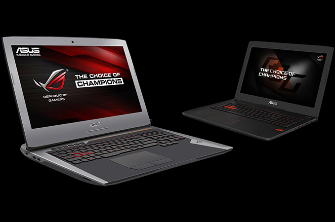
ASUS has unveiled that it is on a new breed of ROG laptops that can be optionally equipped with 120Hz display panels. Several years ago, ASUS and some other vendors already offered notebooks with screens that featured 120 Hz refresh rate along with desktop NVIDIA 3D Vision-ready monitors with similar capability. However, those mobile PCs were pretty rare and barely popular because they relied on TN panels with relatively narrow viewing angles and mediocre color accuracy, as well as because stereoscopic 3D failed to game traction. This time, ASUS will use AU Optronics’ Advanced Hyper-Viewing Angle (AHVA) panels with wider viewing angles and much better IPS-like colors. Furthermore, the main selling point of the new Republic of Gamers laptops will be a combination of NVIDIA’s G-Sync dynamic refresh rate technology with ultra-fast display panels for smooth gaming process.
ASUS plans to offer 120 Hz AHVA panels as an option on its forthcoming 15” and 17” ROG and ROG Strix gaming laptops. In addition to ultra-fast panels, the notebooks will also sport other components you expect from gaming PCs, such as Intel’s Core i7 or Core i5 processors, high-end NVIDIA GeForce GTX graphics adapters (since ASUS specifically mentioned G-Sync in its press release, it is safe to say that the forthcoming notebooks will indeed use NVIDIA graphics), dual-channel DDR4 memory sub-system, M.2 PCIe SSDs, 802.11ac Wi-Fi, specially-designed keyboards and so on. Right now, laptops with display panels featuring 120 Hz refresh rate are a work in progress (ASUS does not even mention their actual resolutions), it is unclear whether the fast AHVA panels will be offered with all ROG models, or only with select ones.
The forthcoming notebooks with display panels featuring 120 Hz refresh rates will be another success for AU Optronics, which was the first to release 144 Hz-capable IPS-like panels for desktop PCs several quarters ago and capitalize on it. As it appears, the company will also be the first to offer high quality 120 Hz-capable AHVA panels for mobile PCs as well.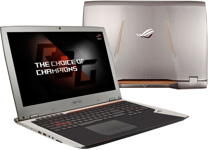
ASUS claims that it will be the first to use high-speed AHVA panels in its mobile PCs. However, if ASUS does not have an exclusive supply agreement with AUO, expect notebooks with screens featuring 120 Hz refresh rates from other manufacturers as well.
ASUS will demonstrate its prototype machines with 120 Hz display panels at Computex, but right now it does not make any promises regarding timeframes of their retail availability, or pricing. As a result, while ASUS seems to be working on appropriate laptops, it does not seem that the company is ready to make any actual announcements. Therefore, we have no idea whether laptops featuring displays with 120 Hz refresh rates will actually be available in high volume in the foreseeable future.
Gallery: ASUS Readies ROG Laptops with 120 Hz AHVA Display Panels


More...
-
-
05-31-16, 09:12 PM #6037
Anandtech: AMD Announces the 7th Generation APU: Excavator mk2 in Bristol Ridge and S
The Carrizo SoC, using Excavator cores, was touted in the press as being the biggest upgrade to the base Bulldozer design since the introduction of Bulldozer itself. This was as a result of new high-density silicon libraries, a new voltage/frequency response unit based on internal sensor data, a redesign of the metal stack to afford high density, improvements to caches and scheduling, improved video units for 4K decode, and a mobile-driven focus for the platform. Today AMD is launching the second version of Excavator, based on an updated core, in two forms: Stoney Ridge for entry level notebooks and Bristol Ridge for mainstream devices.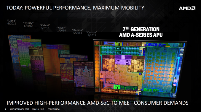
AMD’s future roadmap, at a high level, has been known for some time. First another crack at the Bulldozer architecture, and then we get the new microarchitecture the generation after. On a high-level, that’s a good thing to know. The issue has been that no-one has been able to get hold of deep details, and it does not help when faked slides are posted, outed as fakes, and then reposted continuously anyway. AMD took the lid off their press deck late last week, showing that the last crack at Bulldozer will be mobile driven like the last generation. It should be noted that AMD declined to comment about future desktop platforms at this time.
The 7th Generation APU, in silicon, is by and large similar to the 6th Generation platform called Carrizo with some updates to help drive efficiency and improve performance. This is due to the updated Excavator core, primarily supporting DDR4 memory through the controller (similar to the R-series embedded AMD parts announced earlier), but also tweaks to the 28nm Bulk CMOS physical design that improved the voltage/frequency characteristics of the silicon. This combined with new AVFS (adaptive voltage frequency scaling) algorithms via improved through internal sensors enables AMD to offer a higher frequency for the same Thermal Design Power on the 7th Generation. With this, AMD is claiming that a move from a Kaveri ‘15W’ APU in 2014 to a new Bristol Ridge APU in 2016 can afford a 56% increase in raw CPU performance, or +10% over last year’s Carrizo.AMD APU Generations 1st 2nd 3rd 4th 5th 6th 7th Platform
NameLlano Trinity Kabini Kaveri Beema Carrizo Bristol
StoneyCore K10 / Stars Steamroller Jaguar Piledriver Puma Excavator Released Q2 2011 Q2 2012 Q2 2013 Q1 2014 Q2 2014 Q2 2015 Q2 2016 Market Main Main Entry Main Entry Main Both Top SKU A8-3550MX A10-4657M A6-5200 FX-7600P A8-6410 FX-8800P FX-9830P Threads 4C / 4T 2M / 4T 4C / 4T 2M / 4T 4C / 4T 2M / 4T 2M / 4T Peak MHz 2.7 GHz 3.2 GHz 2.0 GHz 3.6 GHz 2.4 GHz 3.4 GHz 3.7 GHz TDP 45 W 35 W 25 W 35 W 15 W 35W 35 W IGP Family HD 6620G HD 7000 HD 8400 R7 R5 R7 R7 IGP Generation VLIW-5 VLIW-4 GCN 1.0 GCN 1.1 GCN 1.1 GCN 1.2 GCN 1.2 SPs 400
444 MHz384
686 MHz128
600 MHz512
686 MHz128
850 MHz512
800 MHz512
Additional 6/1: AMD has shared with us die sizes and transistor counts. The Bristol Ridge dual module die, including the integrated graphics, comes in at 250.4 mm2 with 3.1 billion transistors. The Stoney Ridge single module die (including IGP) is 124.5mm2 and 1.2 billion transistors.
The improvements to the silicon design, such that a better die can be manufactured, was explained to provide about half the benefit from moving up to the 7th Generation. In this graph, the green line is designed to represent the frequency improvement for the same power between the older Carrizo process and the new Bristol Ridge process.
New in the 7th Generation APU will be what AMD calls 'Shadow Pstates', which AMD is combining with a check at POST on the quality of the silicon. As most silicon dies perform 'around an average point' so to speak, the absolute end AVFS application embedded in the die should need to cover AMD in the case of a bad die in a bad enviroment - this leads to a loss of excess headroom. What AMD will do with 7th Gen is apply a Shadow Pstate (or rather, a differential forced T-state) which allows the AVFS to change depending on the quality, age, degredation and performance of the processor. To put it simply, it allows the AVFS curve to ride nearer each CPU's specific characteristics, rather than a 'one size fits all' approach, and the user will end up with longer boost periods with a high quality die, or use less power when in lower frequency modes (and binning will take this into account).
Another piece in the puzzle is what AMD calls 'Skin Temperature Aware Power Management', which is perhaps a feature that has been on other platforms but AMD has been missing up to now. Despite the unwieldy name, this solution allows an OEM to place up to five sensors over the I2C interface on the SoC and use AMD's internal controller to allow for longer boost periods while the chassis is cool or adjust as necessary. By working with AMD, the OEM's placement of the sensors will allow AMD to suggest appropriate coefficients for their internal controller to respond in the correct way via firmware adjustments.
The big thing to note here, aside from the generational changes in the core, is that AMD is adjusting their mobile strategy. Previously the mobile APU line used low cost, low power ‘cat’ cores such as Bobcat in their entry level products and fatter Bulldozer based cores (like Steamroller and Excavator) in their mainstream line. For the 7th Generation, this goes away with both entry and mainstream parts now going full Excavator, and the two main differences being core count and power window. There’s also some adjustments to the naming of the processors which should help customers and OEMs choose the right part for their workloads.
The baseline platform will be Stoney Ridge, featuring one Excavator module for two threads and support for up to DDR4-2133 in single channel operation. These parts will be +1 GHz compared to the previous cat cores, and feature GCN 1.2 integrated graphics with support for HDMI 2.0, PCIe 3.0, the upgraded video decoder and codec engine, and thus support for VP9 and HEVC decode in AMD’s lowest parts. AMD is also touting a +50% graphics improvement over the last cat core generation at the entry level.
Users will be able to identify Stoney Ridge APUs based on their core count (one module, advertised as dual core), and that the APUs will carry the A9, A6 or E2 branding. The APUs will default to 15W, with only a small configurable TDP window for OEM (except the A9, which can run up to 25W).
The Bristol Ridge platform is for the mainstream. We get an expected dual module design for four threads, support for up to DDR4-2400 but with dual channel operation. Bristol Ridge APUs and Stoney Ridge APUs are the same socket, which means the can be used in the same design similar to Carrizo and Carrizo-L, and back with Carrizo it caused confusion as the high-end part in a platform designed for the low-performance part would only operate in single channel, reducing performance. We double checked with AMD about the whole single/double channel miasma that befell the Carrizo line, and AMD stated that while it is still an OEM decision, they are working closer with OEMs to ensure that users can get a more optimal configuration.
Users will be able to identify Bristol Ridge-based devices by the core count (advertised as quad core), and the APU will be in the FX, A12 or A10 branding. These SKUs will also have a ‘P’ in the name. These APUs will be in two different variants, 15W and 35W, each with a different name to be easily identified. There is a small configurable TDP window for each APU, however the 15W and 35W parts do not overlap.
One device with the 7th Generation APU was actually announced several weeks ago: the HP Envy x360. This device is going to be one of the premium products to use both Bristol Ridge and Stoney Ridge, offering a 360-degree laptop design, a 15.6-inch FHD or UHD display, both PCIe and HDD options, an option for a Windows Hello capable camera, premium audio and up to 10 hours battery life. We expect to see one during Computex this week, but the x360 should be on sale today. We checked with AMD on this too: the x360 will be offered in Stoney Ridge and Bristol Ridge formats, with the latter being dual channel.
The new APU SKUs are split by their FX/A12/A10/A9/A6/E2 branding and thermal design power. The main difference with a change in TDP is going to be the CPU frequency both in base and boost frequency, however some models and cTDP options may adjust the graphics frequency as well.
Each brand will carry ‘7th Gen’ in the image to confirm the use of a *Ridge APU. AMD is stating that APUs equipped with R5 and R7 graphics will allow for dual graphics configurations if the OEMs decide to use a comparable discrete graphics card, and we expect a couple of devices to be launched with this feature.
As the table also shows, users asked for TDP specific product numbers (myself included) and we have them here, especially in the Bristol Ridge parts. Any part that ends in ‘30P’ will be the higher TDP version. Despite this, AMD still offers that cTDP window for each APU, and it is up to the OEM to advertise if this is used. If the Carrizo devices are any indication, OEMs will not state nor will they open the option in the BIOS.
Information on the exact GPU configurations and frequencies should be on its way. We contacted AMD’s PR team after our briefing for this information, and they are sourcing it for us.
Additional 6/1: For the exact graphics configurations, we were given the following:
- FX 9830P: R7, 8 CUs, 512 SPs, 900 MHz max
- FX 9800P: R7, 8 CUs, 512 SPs, 758 MHz max
- A12-9730P: R7, 6 CUs, 384 SPs, 900 MHz max
- A12-9700P: R7, 6 CUs, 384 SPs, 758 MHz max
- A10-9630P: R5, 6 CUs, 384 SPs, 800 MHz max
- A10-9600P: R5, 6 CUs, 384 SPs, 720 MHz max
- A9-9410: R5, 3 CUs, 192 SPs, 800 MHz max
- A6-9210: R4, 3 CUs, 192 SPs, 600 MHz max
- E2-9010: R2, 2 CUs, 128 SPs, 600 MHz max
A story about new AMD products wouldn’t be complete without mentioning gaming bundles. AMD is offering OEM game bundles for any processor that is A9 and up, with the Bristol Ridge parts expanding in their options. It is up to the OEM to take on this offer and pass it on to the customer, so mileage on which products will offer this will vary.
Final Thoughts
Despite many users believing that AMD would be discussing AM4 and their desktop versions of Bristol Ridge at Computex, the opposite seems to be the case. AMD isn’t discussing it, and I’ve hit a solid wall with the motherboard manufacturers as well. If rumors are to be believed, based on a CPU cooling company Facebook post that was deleted, the socket is mostly likely the same dimensions as AM2/AM3, however we can’t even verify that. It would seem that whatever your prediction for hearing about new desktop products was, add at least a quarter.
But put this into perspective here. Bristol Ridge is still based on Excavator – a core that was initially designed to run at 15W in dual-module configuration. AMD stated at the Tech Day in 2015 that the higher TDP/frequency you run a Carrizo platform, the lower the differential to a 2014 Kaveri platform. AMD teased Carrizo on the desktop with the Athlon X4 845 at 65W for the FM2+ socket (and I apologize that I haven’t got around to writing the review fully yet), however this was one part without integrated graphics and a very low-frequency ceiling when overclocking. Despite this, Carrizo on the desktop was still a surprising performer, but only at the low powered part of the product stack. If we’re going to see Carrizo mk2 and Bristol Ridge on the desktop, it might only be for those lower power 35W-45W parts, and there’s no point releasing a platform with just 45W parts if it is going to evolve into the extreme platform with a Zen drop in: you need both, especially if each one is designed for specific markets. There’s an obvious line of thought I’m going down here, and while I won’t say it outright, the signs are getting less fuzzy as time moves on.
Desktop aside, we reviewed the OEM implementations of AMD’s Carrizo platform earlier this year and came away feeling that an opportunity to show off the hardware had been missed. I know that AMD took on board our points and discussed them internally, and hopefully working with HP on the x360 can show what the APUs should be able to do. We expect to see more 7th Generation device announcements at Computex this week, and I’ll ping AMD and HP for some hands-on time with a review unit in due course.
Gallery: AMD Announces the 7th Generation APU: Excavator mk2 in Bristol Ridge and Stoney Ridge for Notebooks


More...
-
05-31-16, 10:36 PM #6038
Anandtech: AMD Briefly Shows Off Zen Summit Ridge Silicon
After an already packed Computex 2016 event with Radeon Polaris and Bristol Ridge/Stoney Ridge news, AMD CEO Dr. Lisa Su had one final surprise to close out the company’s presentation: Zen, in the flesh.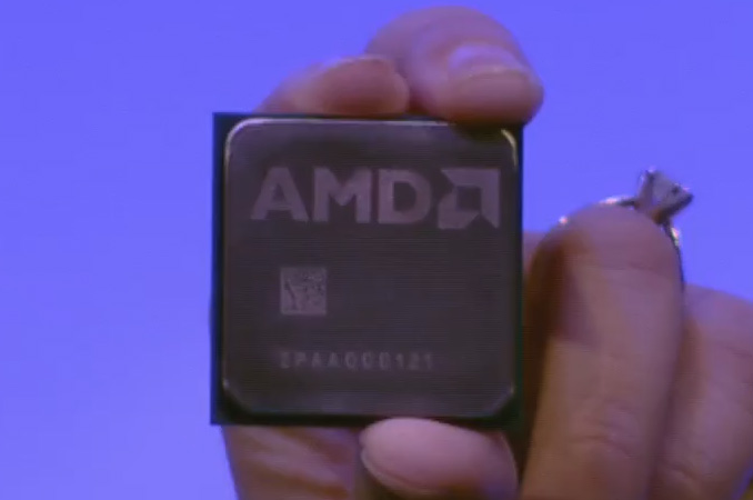
Zen taped out earlier this year, and AMD is now working on bringing it up in their labs. To that end Dr. Su pulled out a very early engineering sample of what will be AMD’s Summit Ridge CPU, an 8 core Zen-based CPU. Summit Ridge will use AMD’s new AM4 socket – currently being rolled out for Bristol Ridge – making it a drop-in platform replacement.
Little in the way of new details on Summit Ridge and Zen were released, but Dr. Su confirmed that AMD is still targeting a 40% IPC increase. On the development front, the chip still has some work to undergo, but AMD is to the point where they are going to start sampling their top-tier, high profile customers with engineering samples here in a few weeks. Wider sampling to their larger OEM base will in turn take place in Q3 of this year. AMD has not mentioned a retail product date, but keep in mind there’s a fairly significant lag time between OEM sampling and retail products.
Finally, Dr. Su also reiterated that Zen will be the basis of a range of products for AMD. Along with the desktop CPU, AMD will be using Zen as the basis of their next, 8th generation APU. And further down the line it will be appearing in server products and embedded products as well.
More...
-
06-01-16, 07:37 AM #6039
Anandtech: Qualcomm Announces Snapdragon Wear 1100 SoC For Wearables
Qualcomm introduced the Snapdragon Wear 1100 SoC today at Computex 2016. Intended for wearable devices, such as fitness trackers, smart headsets, and connected watches for children, it features a single ARM Cortex-A7 CPU running at up to 1.2GHz and a fixed-function GPU for rendering simple 2D user interfaces. It's interesting that Qualcomm chose to stick with the A7 rather than use its replacement: the Cortex-A35. According to ARM, the A35 uses 10% less power while boosting performance between 6-40% at the same frequency and on the same process. This could simply be a matter of timing or just Qualcomm's familiarity with the A7.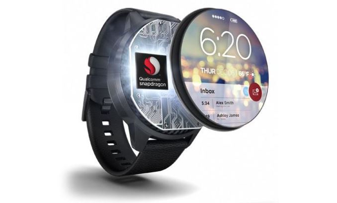
The Snapdragon Wear 1100 is a compliment to the Snapdragon Wear 2100 SoC that Qualcomm announced back in February 2016, and is meant to run lean, Linux-based operating systems instead of Android or Android Wear, which require the performance of the 2100 to deliver richer, more graphical experiences like those in typical smartwatches.
The Snapdragon Wear 1100 integrates a Category 1 LTE modem that supports LTE FDD, LTE TDD, TD-SCDMA, and GSM networks with global frequency band support for keeping devices connected independent of a companion device such as a smartphone. Customers can also choose to incorporate Wi-Fi and Bluetooth connectivity options. Another feature crucial for safety monitoring applications that use geo-fencing is the inclusion of Qualcomm’s iZat Gen 8C location engine that supports the GPS, GLONASS, Galileo, and BeiDou positioning satellite networks. Location accuracy and speed are improved by augmenting GNSS with Wi-Fi and cellular networks.
The Snapdragon Wear 1100’s package size is 79mm², including the modem, RF transceiver, and PMIC, and is manufactured on a 28nm LP process. Also included in the package is a low-power sensor hub and a hardware cryptographic engine, features that further reduce power consumption. When paired with a 350mAh battery, Qualcomm claims the Snapdragon Wear 1100 allows for up to 7-days of LTE standby.Qualcomm Snapdragon Wear SoCs Snapdragon Wear 1100 Snapdragon Wear 2100 SoC Cortex-A7 @ 1.2GHz (256KB L2)
fixed-function GPU4x Cortex-A7 @ 1.2GHz
Adreno 304 (OpenGL ES 3.0)Process Node 28nm LP 28nm LP RAM LPDDR2 LPDDR3-800 MT/s Display Simple 2D UI Up to 640x480 @ 60fps Modem Qualcomm (Integrated)
2G / 3G / 4G LTE (Category 1 10/5 Mbps)Qualcomm X5 (Integrated)
2G / 3G / 4G LTE (Category 4 150/50 Mbps)
Connected version onlyConnectivity 802.11b/g/n/ac, BT 4.1 LE, GPS/GLONASS/Galileo/BeiDou
(Wi-Fi and BT optional)802.11b/g/n (2.4GHz), BT 4.1 LE, NFC, GPS/GLONASS/Galileo/BeiDou, USB 2.0
Connected and Tethered versions
Wearables featuring the higher-performing Snapdragon Wear 2100 SoC should be available in the second half of 2016, while the Snapdragon Wear 1100 is available to ODMs starting today.
More...
-
06-01-16, 08:30 AM #6040
Anandtech: The 9.7" iPad Pro Review
In late 2015 Apple launched a tablet that they called the iPad Pro. It had been rumored for quite some time, and it had a number of features that differentiated it from other iPads. The most notable was its 12.9" display, which has a width equal to the height of Apple's 9.7" iPads, allowing it to use two essentially full sized iPad applications at the same time in a split screen view. In addition to its massive display, the iPad Pro came with two accessories that had not existed for any prior iPad. It seemed that in Apple's eyes the Apple Pencil and the Smart Keyboard really defined what made the iPad Pro worthy of the "Pro" name. Now Apple has launched a second iPad Pro to fill in the ten inch tablet market. Read on for the full review of the 9.7" iPad Pro.
More...


 Quote
QuoteThread Information
Users Browsing this Thread
There are currently 25 users browsing this thread. (0 members and 25 guests)


Bookmarks