

Results 6,171 to 6,180 of 12096
Thread: Anandtech News
-
07-29-16, 09:17 AM #6171
Anandtech: AMD Releases Radeon Software Crimson Edition 16.7.3
AMD's Radeon Technologies Group has released another driver update with a healthy list of fixes. On the list today are fixes for CrossFire, flickering in both rendering and the display, and some general stability and bugs. Along with fixes we also see a hefty performance bump in Tomb Raider on AMD’s latest Radeon RX 480.
?Radeon Software Crimson Edition 16.7.3 brings us up to driver version 16.30.2311, which indicates that this is likely a new driver branch for AMD. Accordingly, despite the deceptive Radeon Software version number, this release contains a relatively large number of performance improvements nad bug fixes.
First up, AMD has provided more fixes for Crossfire users. These include a fix for Overwatch crashing in some RX 480 configurations while using Crossfire, and some flickering in both Rise of the Tomb Raider and Need for Speed. A number of flicker fixes have also been made, including a fix for DiRT Rally for terrain flickering when advanced blending is enabled, and some general flickering issues when launching/exiting games on an RX 480 + Freesync display setup.
The rendering fixes are not over yet though. A graphical corruption issue with Hitman in DX12 mode has been fixed, as has texture corruption with Total War: Warhammer on a Radeon R9 380. An occasional shadow rendering issue when using DOTA 2 with the Vulkan API has been fixed as well, as has a texture issue with Doom in OpenGL mode on an Eyefinity display setup..
To wind up the list of fixes this time around, AMD has also fixed some bugs in their control panel. This includes an issue where Vukan information in Radeon Settings could display an incorrect version number, and a bug where Radeon Wattman could retain settings of an overclock even after it had failed.
For performance improvements we get to see a 10% improvement in performance for Rise of the Tomb Raider on the Radeon RX 480. According to AMD's notes, this test was done on a system running an Intel i7-5960X at 1080p, resulting in the score climbing from 78.73 to 86.53. Of course, a grain of salt should be served with benchmarks from a vendor. On the other hand, 10% is far enough beyond margin of error that many configurations, at least those running an RX 480, should see at least some noticeable benefit.
As always, those interested in reading more or installing the updated hotfix drivers for AMD’s desktop, mobile, and integrated GPUs can find them either under the driver update section in Radeon Settings or on AMDs Radeon Software Crimson Edition download page.
More...
-
07-29-16, 09:17 AM #6172
Anandtech: NVIDIA Agrees To Proposed GeForce GTX 970 Class Action Settlement: US Buye
(Personal note: I generally prefer not to post news about class action settlements, as I find that these days they rarely establish truth or justice, and instead mostly benefit law firms while everyone tries to settle the issue without admitting any wrongdoing. That said, GTX 970 was one of NVIDIA’s most popular cards, so this is going to impact a lot of our readers in the US)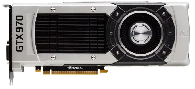
Word comes from Top Class Actions (via The Tech Report) that NVIDIA will soon be settling a series of proposed class action lawsuits brought against the company regarding the GeForce GTX 970. Under the preliminary settlement, United States residents who purchased GeForce GTX 970 cards would be able to claim a $30 settlement in return for dropping further litigation against the company. With the GTX 970 having launched at $329, this amounts to a de facto 9% rebate on the card.
The class action suits in question were brought against the company almost immediately after NVIDIA made the important (and more than a bit painful) disclosure that the initially published specifications for the GTX 970 were wrong. Specifically, that the card had an unusual memory crossbar organization where one ROP/L2 partition was disabled, giving the card only 56 ROPs instead of 64. Furthermore, this meant that the last 512MB of the standard 4GB of VRAM could not be accessed in a contiguous manner, impacting how it could be used. To that end, as the Top Class Actions article notes, the $30 settlement “was calculated to represent a portion of the cost of the storage and performance capabilities the consumers thought they were obtaining in the purchase of the product.”
With that said, at this point the settlement itself has yet to be approved by the court, and signups are not yet available. Assuming it is approved, I’d expect that signups will be made available shortly thereafter.
More...
-
07-29-16, 03:44 PM #6173
Anandtech: Patriot Adds Two Dual-Channel DDR4-3733 Memory Kits into Lineup
Patriot this week unveiled two new DDR4 kits rated to run at DDR4-3733. The dual-channel kits are designed for Intel’s latest platforms and belong to Patriot’s Viper Elite and Viper 4 families. The new DDR4-3733 memory modules will be the fastest in Patriot’s lineup.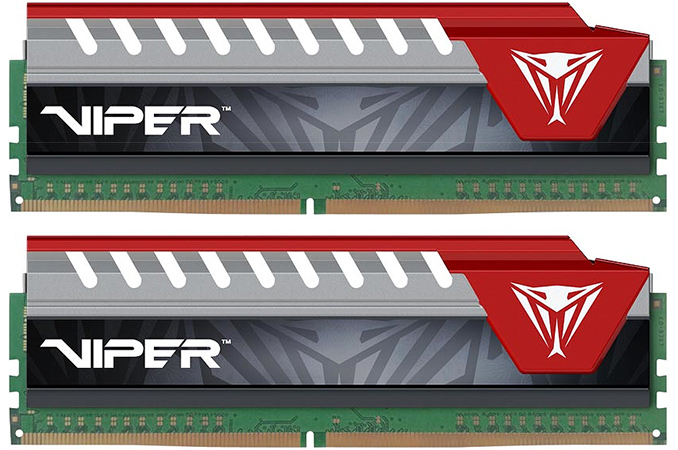
Patriot’s new Viper Elite and Viper 4 dual-channel memory kits are rated to run at 3733 MT/s with CL17 19-19-39 timings at 1.35 V. The sets consist of two 8 GB modules, which use modern 8 Gb memory ICs (integrated circuits) from an undisclosed manufacturer. The new modules are designed for Intel’s 100-series platforms and come with XMP 2.0 profiles to make it easier for end-users to run them at their rated specifications with the right timings and voltage.
The difference between the Viper Elite and the Viper 4 modules in all in the look. Typically, Patriot positions its Viper Elite products below the Viper 4, and aims them at modders. These modules come with heatsinks of three different colors (red, blue and grey). The Viper 4 family typically focuses on the faster segments and features red extruded aluminum heatsinks. Nonetheless, in this particular case both the Viper Elite DDR4-3733 devices also come only with silver and red heatsinks. Therefore, the difference between two types of DDR4-3733 solutions from Patriot lies only in aesthetics and dimensions.Specifications of Patriot's DDR4-3733 Kits Module Capacity Kit
CapacityLatencies Voltage Height Part Number Viper Elite 8 GB 16 GB 17-19-19-39 1.35 V 43.0 mm PVE416G373C7KRD Viper 4 42.6 mm PV416G373C7K
Patriot’s Viper 4 and Viper Elite 16 GB (2 x 8GB) DDR4-3733 dual-channel memory kits will be available for purchase online and in stores starting from August 3 for the recommended price of $159.99.
Only a few memory module makers offer DDR4 sticks rated to run above 3400 MT/s speeds because it requires sufficient binning, as well as an appropriate volume of sales to make it worthwhile. It gets rather tricky to cherry pick a sufficient amount of such ICs to build appropriate products. The fact that Patriot rolled out two DDR4-3733 kits indicates that the company is willing to compete for very high-end systems featuring fast memory as well as showing the ability of mass-produced DDR4 chips to run at higher frequencies.
More...
-
07-29-16, 04:19 PM #6174
Anandtech: Samsungs PM1633a Now Available: $10k for 15 TB, $6k for 7 TB
Samsung started to ship its PM1633a SSD with 15.36 TB capacity to select customers in March and recently it began to supply the drive to select resellers as well. The enterprise-class SSD is now offered by two U.S.-based retailers and can be purchased for ~$10,000, which makes it one of the world’s most expensive commercial solid-state drives. Meanwhile, Samsung officially expanded its PM1633a family of SSDs with many lower-capacity models and has begun to ship the 7.68 TB version to at least one reseller.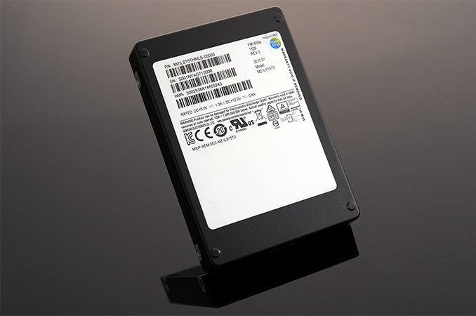
The Samsung PM1633a drives are based on the company’s third-generation 256 Gb TLC 3D V-NAND memory chips introduced last year. Samsung stacks 16 of such ICs to form a single 512 GB package and then uses 32 of them to build its flagship 15.36 TB SSD, leaving about 1 TB of NAND flash for overprovisioning. Typically, high-capacity SSDs do not provide very high performance, because of peculiarities of their internal architecture and limitations of contemporary controllers (which cannot simultaneously access many high-density chips, or multiple controllers in a RAID-0 stripe configuration). To speed up its most spacious PM1633a drive, Samsung had to develop a new proprietary controller that can concurrently access large amounts of high-density NAND flash with the help of a special firmware. For its flagship PM1633a 15.36 TB SSD, the manufacturer declares sequential read performance up to 1200 MB/s as well as sequential write performance up to 900 MB/s using the SAS-12Gbps interface. As for random read and write operations, the 15.36 TB SSD can deliver up to 195,000 and 31,000 IOPS respectively (which is slightly lower than the company advertised back in March).
When Samsung announced its PM1633a SSD earlier this year, it only introduced one model with 15.36 TB capacity. Since then, the company has officially expanded the PM1633a family with 480 GB, 960 GB, 1.92 TB, 3.84 TB and 7.68 TB models (see flyer for details). The expansion of the lineup demonstrates Samsung’s confidence that its third-generation V-NAND TLC memory is reliable enough for enterprise usage scenarios. In fact, the PM1633a series consists of six SKUs, whereas the PM1633 family based on the second-gen 32-layer V-NAND includes only four configurations (up to 3.8 TB capacity, but they are faster than the PM1633a). Both lineups are aimed at enterprise storage applications with SAS 12Gbps interface.
Back in March, Samsung only began to ship its PM1633a to select clients. We suspect that these clients are those that run large cloud data centers, and require such drives to run their specific workloads. Now,the manufacturer has started to ship its flagship SAS SSD to a broader range of customers. For example, the Samsung PM1633a 15.36 TB drive (MZILS15THMLS) is now offered by CDW for $10,311.99 as well as by SHI for $9,690 on preorder. Both retailers ask to contact them for actual availability, depending on when stock is available (which is not surprising, given the price of the SSD as well as its very special positioning). In addition, CDW also offers the PM1633a 7.68 TB (MZILS7T6HMLS) drive for $5,729.99, which ships within 11–13 days.Samsung PM1633a SSD General Specifications Capacity 480 GB, 960 GB, 1.92 TB, 3.84 TB, 7.68 TB, 15.36 TB Controller Samsung proprietary controller NAND Samsung's 256 Gb 48-layer TLC NAND DRAM Cache up to 16 GB DDR3 SDRAM (15.36 TB model) Sequential Read 1200 MB/s Sequential Write 900 MB/s Random Read up to 195,000 IOPS (15.36 TB model) Random Write up to 31,000 IOPS (15.36 TB model) Power Consumption (active/idle) 11W/4.5W (15.36 TB model) MTBF 2,000,000 hours Endurance 1 DWPD (Drive Writes Per Day) Power Loss Protection Based on tantalum capacitors Warranty 5 Years Interface and Form-Factor 2.5"/15mm SAS-12 Gbps (15.36 TB model)
The price of Samsung’s PM1633a 15.36 TB SSD may seem excessive, but for large cloud data centers (which always try to maximize their storage capacity) as well as mission-critical storage applications such drives make a lot of sense. For example, Supermicro has 2U machines that can fit in 48 SAS3/12G storage devices (1, 2). Each of such servers can store 737.28 TB of data (if fully populated with Samsung’s 15.36 TB SSDs), whereas storage capacity of a 42U cabinet featuring 21 of such servers will be 15482 TB (15.4 PB). By contrast, a standard 42U storage rack featuring 360 3.5” 10 TB hard drives can store around 3600 TB. Moreover, given very high sequential and random read/write performance of the PM1633a, just one such device can substitute many 10K or 15K mission-critical HDDs (each of which can cost $400 – $700). Hence, there will be numerous customers interested in buying the Samsung PM1633a 15.36 TB for its price-point.
Sources: Samsung, CDW (via PC World), SHI.
Gallery: Samsung Expands Its PM1633a Lineup As 15.36 TB SSD Hits Retail for $10K


Other Reading:
The Samsung 850 EVO 4TB SSD Review
Samsung's 850 EVO 4TB Now Available at $1500
More...
-
08-01-16, 04:21 AM #6175
Anandtech: Hidden Secrets: Investigation Shows That NVIDIA GPUs Implement Tile Based
As someone who analyzes GPUs for a living, one of the more vexing things in my life has been NVIDIA’s Maxwell architecture. The company’s 28nm refresh offered a huge performance-per-watt increase for only a modest die size increase, essentially allowing NVIDIA to offer a full generation’s performance improvement without a corresponding manufacturing improvement. We’ve had architectural updates on the same node before, but never anything quite like Maxwell.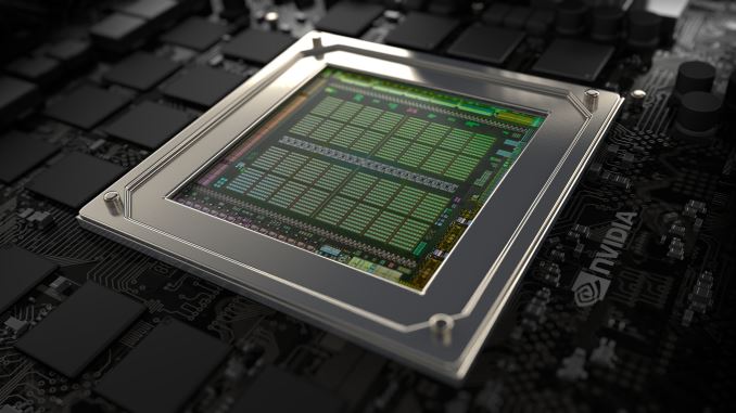
The vexing aspect to me has been that while NVIDIA shared some details about how they improved Maxwell’s efficiency over Kepler, they have never disclosed all of the major improvements under the hood. We know, for example, that Maxwell implemented a significantly altered SM structure that was easier to reach peak utilization on, and thanks to its partitioning wasted much less power on interconnects. We also know that NVIDIA significantly increased the L2 cache size and did a number of low-level (transistor level) optimizations to the design. But NVIDIA has also held back information – the technical advantages that are their secret sauce – so I’ve never had a complete picture of how Maxwell compares to Kepler.
For a while now, a number of people have suspected that one of the ingredients of that secret sauce was that NVIDIA had applied some mobile power efficiency technologies to Maxwell. It was, after all, their original mobile-first GPU architecture, and now we have some data to back that up. Friend of AnandTech and all around tech guru David Kanter of Real World Tech has gone digging through Maxwell/Pascal, and in an article & video published this morning, he outlines how he has uncovered very convincing evidence that NVIDIA implemented a tile based rendering system with Maxwell.
In short, by playing around with some DirectX code specifically designed to look at triangle rasterization, he has come up with some solid evidence that NVIDIA’s handling of tringles has significantly changed since Kepler, and that their current method of triangle handling is consistent with a tile based renderer.
Tile based rendering is something we’ve seen for some time in the mobile space, with both Imagination PowerVR and ARM Mali implementing it. The significance of tiling is that by splitting a scene up into tiles, tiles can be rasterized piece by piece by the GPU almost entirely on die, as opposed to the more memory (and power) intensive process of rasterizing the entire frame at once via immediate mode rendering. The trade-off with tiling, and why it’s a bit surprising to see it here, is that the PC legacy is immediate mode rendering, and this is still how most applications expect PC GPUs to work. So to implement tile based rasterization on Maxwell means that NVIDIA has found a practical means to overcome the drawbacks of the method and the potential compatibility issues.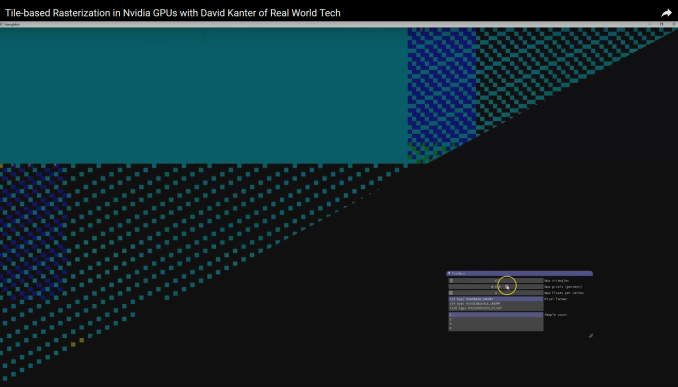
NVIDIA Maxwell Architecture Rasterization Tiling Pattern (Image Courtesy: Real World Tech)
In any case, Real Word Tech’s article goes into greater detail about what’s going on, so I won’t spoil it further. But with this information in hand, we now have a more complete picture of how Maxwell (and Pascal) work, and consequently how NVIDIA was able to improve over Kepler by so much. Finally, at this point in time Real World Tech believes that NVIDIA is the only PC GPU manufacturer to use tile based rasterization, which also helps to explain some of NVIDIA’s current advantages over Intel’s and AMD’s GPU architectures, and gives us an idea of what we may see them do in the future.
More...
-
08-01-16, 08:33 AM #6176
Anandtech: The Alphacool Eisbaer 240 CPU AIO Liquid Cooler Review
Alphacool has been a known manufacturer of liquid cooling products for many years but had virtually no presence in the mainstream market until recently. In this review we are having a look at the company’s first AIO liquid cooling CPU cooler, the Eisbaer. This is a product targeted at a wide audience of users, but that also faces a lot of competition from numerous other products.
More...
-
08-01-16, 09:31 AM #6177
Anandtech: SK Hynix Adds HBM2 to Catalog: 4 GB Stacks Set to Be Available in Q3
SK Hynix has quietly added its HBM Gen 2 memory stacks to its public product catalog earlier this month, which means that the start of mass production should be imminent. The company will first offer two types of new memory modules with the same capacity, but different transfer-rates, targeting graphics cards, HPC accelerators and other applications. Over time, the HBM2 family will get broader.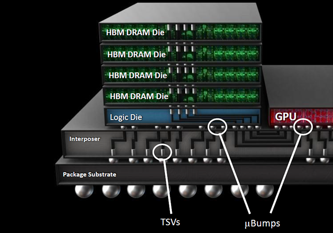
SK Hynix intends to initially offer its clients 4 GB HBM2 4Hi stack KGSDs (known good stack dies) based on 8 Gb DRAM devices. The memory devices will feature a 1024-bit bus as well as 1.6 GT/s (H5VR32ESM4H-12C) and 2.0 GT/s (H5VR32ESM4H-20C) data-rates, thus offering 204 GB/s and 256 GB/s peak bandwidth per stack. Earlier this year a representative for SK Hynix revealed plans (in an interview with Golem.de) to start volume production of 4 GB HBM2 KGSDs in Q3 and the addition of the devices into product catalog confirms this information. Keep in mind that memory companies usually make announcements about the start of mass production when they are ready to deliver the first batch of new DRAM to a customer(s). Therefore, it is possible that SK Hynix may already be producing HBM2 stacks.
As outlined in our article published earlier this year, HBM2 memory can stack two, four or eight DRAM devices (2Hi, 4Hi, 8Hi stacks) interconnected using through silicon vias (TSVs) on a base logic die per KGSD (known good stacked die). Each DRAM device features two 128-bit channels, which use DDR signaling with a 2n prefetch architecture (256 bits per memory read and write access) and can operate at their own frequency or even in their own mode. SK Hynix uses 21 nm process technology to make its HBM2 memory and eventually plans to offer 2 GB and 8 GB KGSDs (featuring two or eight 8 Gb DRAM ICs) in addition to 4 GB stacks, aimed at providing memory for various applications. All HBM2 memory products from the company will have 1.2 V VDD/VDDQ and will come in new packages featuring 7.75 mm × 11.87 mm (91.99 mm2) dimensions.Specifications of SK Hynix's HBM2 Memory Chips Part Number Density Data Rate Bandwidth
per StackPackaging Feature Availability H5VR32ESM4H-20C 4 GB 2.0 GT/s 256 GB/s 5mKGSD 4Hi stack, VDD/VDDQ=1.2V Q3'16 H5VR32ESM4H-12C 1.6 GT/s 204 GB/s
Samsung Electronics began to mass produce its 4 GB 4Hi stack HBM2 KGSDs featuring 2 GT/s data-rate earlier this year and NVIDIA employed the new chips for its GP100 GPU. The first NVIDIA-branded card to use the HBM2 is the Tesla P100 compute accelerator, which has 16 GB of HBM2 memory with 720 GB/s bandwidth (as the DRAM interface operates at about 1.4 GT/s data-rate).
Speaking of HBM2 usage by commercial SoCs, last year SK Hynix said that it worked with 10 companies on various projects (including ASICs, x86 processors, ASSPs and FPGAs) featuring HBM memory (both generations), which indicates that the interest for multi-layer high-bandwidth DRAM is here. However, so far only AMD and NVIDIA have introduced actual products featuring HBM and HBM2.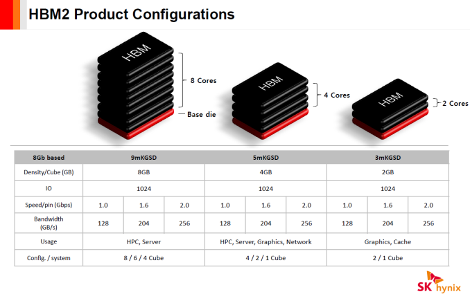
When it comes to the original HBM, it is worth to mention that SK Hynix has removed such stacks from its catalog. It is unknown whether the company continues to ship them to interested parties, but given the fact that there are not a lot of products that utilize HBM1 today, small scale shipments should not be a problem (at least, until SK Hynix phases out its 29 nm production lines). Meanwhile, since HBM2 is here, it is feasible to assume that we are not going to see many new devices utilizing HBM1.
More...
-
08-02-16, 07:08 AM #6178
Anandtech: Windows 10 Anniversary Update: The Road To Redstone
It’s already been a year since Microsoft launched Windows 10, and we have had a couple of updates since release. The biggest update yet though is the Windows 10 Anniversary Update, which was codenamed Redstone throughout its development. It’s the first major branch from the launch codebase and with it Microsoft has added a lot of new features, polished some of the interface, and has overall provided a nice update to those on Windows 10.
More...
-
08-02-16, 10:08 AM #6179
Anandtech: Hands On With the Samsung Galaxy Note7
The Galaxy Note line is a staple at this point, a segment that Samsung truly owns as the first mover and has been wildly successful in ways that Samsung really didn’t predict. The Galaxy Note line has often been said to be the true flagship of the Galaxy smartphone family, and to some extent that probably isn’t far off the mark. With the Galaxy Note7, Samsung is seeking to better indicate that status by bringing it up to the same generation as the Galaxy S7.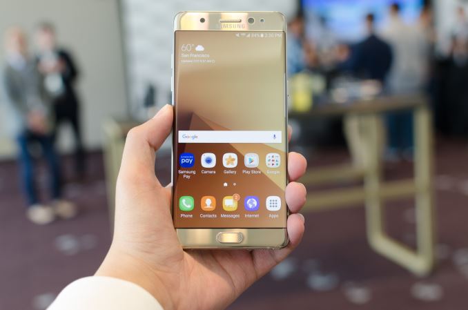
Of course, the number is just part of a name, so to see whether the Galaxy Note7 lives up to its promise as the flagship of the Galaxy line we can start with some basic specs.
At a high level, there’s really not a lot that changes relative to the Galaxy S7 family. The same Exynos 8890 and Snapdragon 820 SoCs are used in the same regions as the Galaxy S7. The cameras are the same as well. Really, it’s easier to talk about what sets the Galaxy Note7 apart than the similarities as there is a lot of common ground here. Relative to the Galaxy S7 edge, the Note7 gains the S-Pen, a slightly larger 5.7 inch dual-edge display, and has a slightly smaller 13.48 WHr battery. The Note7 also gains a USB type C port.Samsung Galaxy Note5 Samsung Galaxy Note7 SoC Exynos 7420
4x Cortex-A57 @ 2.1Ghz
4x Cortex-A53 @ 1.5GHz
Mali T770MP8
(Samsung 14LPE)Snapdragon 820 (US)
2x Kryo @ 2.15GHz
2x Kryo @ 1.6GHz
Adreno 530
Exynos 8890 (ROW)
4x Exynos M1 @ 2.3GHz
4x Cortex A53 @ 1.6GHz
Mali T880MP12
(Samsung 14LPP)RAM 4GB LPDDR4 4GB LPDDR4 NAND 32/64/128GB NAND (UFS 2.0) 64GB NAND (UFS 2.0) + microSD Display 5.7” 1440p
SAMOLED5.7” 1440p
SAMOLED Dual EdgeNetwork 2G / 3G / 4G LTE (Category 6/9 LTE)
Region Dependent2G / 3G / 4G LTE (Category 12/10/9 LTE)
Region DependentDimensions 144.6 x 69.7 x 9.61mm, 157g 153.5 x 73.9 x 7.9mm, 169g Camera 16MP Rear Facing w/ OIS f/1.9, 1.12µm, 1/2.6"
(Sony IMX240, Samsung S5K2P2)12MP Rear Facing w/ OIS, f/1.7, 1.4µm, 1/2.6"
(Sony IMX260, Samsung S5K2L1)5MP Front Facing, f/1.9, 1.12µm
(Samsung S5K4E6)5MP Front Facing, f/1.7, 1.12µm
(Samsung S5K4E6)Battery 3000 mAh (11.55 Whr) 3500 mAh (13.48 Whr) OS Android 5 w/ TouchWiz
(At Launch)Android 6 w/ TouchWiz
(At Launch)Connectivity 2x2 802.11a/b/g/n/ac,
BT 4.2
USB-C, USB?,
GPS/GLONASS/Beidou
NFC, MST2x2 802.11a/b/g/n/ac,
BT 4.2
USB-C, USB?,
GPS/GLONASS/Beidou
NFC, MSTFingerprint Sensor Capacitive by Synaptics Capacitive by Synaptics SIM NanoSIM NanoSIM
While it may be easy to get caught up on the slightly reduced battery capacity of the Note7 relative to the S7 edge, realistically the delta is solely due to the addition of the S-Pen. The camera hump is basically already nonexistent on these phones, so I’m not sure it necessarily makes a lot of sense to make the battery even larger when the cost will likely come in the form of a larger phone overall. Based on Samsung’s consumer research, one of the single biggest requests from users was to fit the biggest possible display into the smallest possible phone, so jumping up to something like 15 WHr would likely compromise that goal.
In a lot of ways, the Galaxy Note7 attempts to try and refine the Galaxy S7 edge, and one of the notable ways that Samsung has done this is refining the design. Samsung emphasized the amount of symmetry present in this design, and almost everything is aligned in this phone unlike the Galaxy S7. The Galaxy S7 felt like it wasn’t all that cohesive in general with things like the USB port misaligned with the speaker port and 3.5mm headphone jack, so this is actually a notable difference although I’m not sure this would really make a sale one way or another.
The more obvious way that design has been emphasized with the Galaxy Note7 is the total lack of a flat display variant, which was done in an effort to respond to the demand to make the device smaller. There’s really no doubt that the Galaxy Note7 is a smaller phone now as the width of the phone has been reduced by 3mm relative to the Galaxy Note5, and is almost identical in other dimensions and weight. That’s basically as far as the functional aspect of the edge display goes, and Samsung was fairly clear in their messaging that the edge display is just aesthetically better. They’re definitely not wrong here, but if you like using screen protectors the only way to cover the display will be with wet-application TPU-based protectors. Of course, Gorilla Glass 5 is on the front to help reduce the likelihood of damage but given that scratch resistance against ubiquitous quartz sand is still not going to be amazing you’ll still want a screen protector if microscratches bother you.
By using the edge display and 3D curved glass on the back, the design of the Galaxy Note7 is notably symmetrical when you look at its side profile, which is actually a pretty neat effect. For whatever reason the display of the Galaxy Note7 doesn’t have the normal green tint at the edges that I’ve come to expect from the S7 edge. According to Samsung the curvature has been adjusted somewhat relative to the Galaxy S7 edge which is what results in the difference in viewing angles. The display is otherwise identical in terms of performance and efficiency, with the sole exception of a new HDR display mode that allows maximum brightness to go as high as 600 nits in high APL conditions for short periods of time. This is contrasted with the outdoor brightness boost function which is closer to 500 nits. Based on conversations with those at Samsung it seems that this mode can only be unlocked by a few specific applications like Amazon’s Prime Video app, but I’m sure that with enough digging around in the system it will be possible to figure out the API that allows for controlling this functionality for third party HDR video playback.
Continuing with the design theme, the software of the Note7 has seen major revisions with a new version of TouchWiz that looks to incorporate better iconography and better overall design. Of course, it’s hard to say whether the device has been made smoother or faster here, but that’s something best left to the full review. There are also some notable new software features like a secure folder that uses Knox’s secure container APIs to allow photos, notes, and other app information to be stored separately with fingerprint or iris authentication.
While we’re still on the subject, it’s worth mentioning that Samsung has added iris authentication on the Note7 which is probably not a surprise if you follow any of this closely. It seems to work well and uses IR light to make sure it works in low light but it’s important to note that this system has a somewhat low preview frame rate and can only use one set of eyes for registration. It also notes a number of limitations in the UI but doesn’t actually require you to take off your glasses or contacts even though it suggests these things in the UI. The iris scanner also works at about 10-14 inches away from the eye which is kind of surprising and leads me to believe that this may be closer to some advanced facial recognition with a wide and narrow angle lens to capture the face and eyes rather than true iris scanning.
The other new software feature added is the ability to turn videos into GIFs with the S-Pen. Samsung representatives noted that this only works with non-DRM video, so I’m guessing that YouTube won’t necessarily work 100% of the time here although capturing videos taken by the camera definitely will. There’s also the ability to dynamically translate text selected by the S-Pen and take notes with the Always-On Display feature. Samsung has also wisely combined the mishmash of note-taking applications with the previous generations of Galaxy Note phablets and replaced them with a single Samsung Notes application to improve user experience.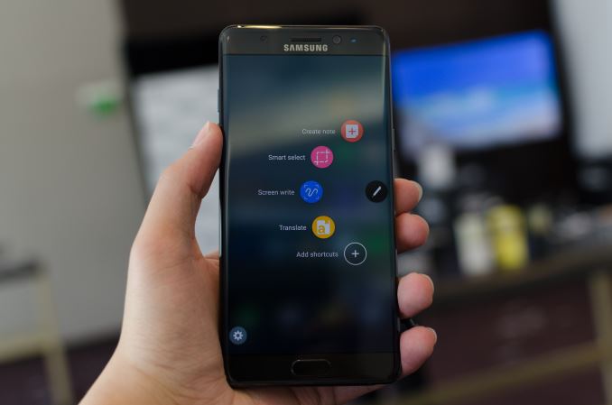
On the hardware side, the S-Pen has been redesigned so that the phone is not damaged if you decide the stick the S-Pen in backwards for whatever reason, and a smaller 0.7mm tip with double the pressure sensitivity of the Note5. The device is still fully IP68 compliant whether the S-Pen is attached or detached, so you can theoretically take notes with the phone in a bathtub or something similar. As the S-Pen uses licensed Wacom magnetic resonance technology, it maintains full accuracy and sensitivity in the presence of water unlike partially capacitive solutions like the Apple Pencil.
Outside of the device itself, Samsung is including new accessories like an IP68 compliant wireless charging battery case, and an S View standing cover that makes it easy to prop up the device when it’s on a desk as Samsung noticed in their user studies that people often wanted to watch content without holding the device, with various implements used to achieve that goal.
If you want the Galaxy S7 edge with an S-Pen, the Galaxy Note7 looks to be that and a bit more as far as software and overall design goes. It’ll be important to see how it does in the review but honestly given Samsung’s track record I would be surprised to discover anything out of the ordinary with the Note7.
The Galaxy Note7 will be available in Blue Onyx, Silver Titanium, and Black Onyx in the US on AT&T, Sprint, T-Mobile USA, US Cellular, and Verizon in stores starting August 19 and preorders starting on August 3. An updated companion Gear VR with USB-C support and a slightly wider 101 degree FOV along with a dark blue design will also be available with the same dates for preorder and general release.
More...
-
08-02-16, 01:07 PM #6180
Anandtech: Crucial Expands MX300 SSD Lineup with Additional Capacities: Up to 1TB
Crucial this week made two announcements. Its MX300 family of 3D NAND-based consumer-grade SSDs has been expanded with additional models, and also Crucial revealed plans to start sales of its MX300 drives in the M.2 form-factor. The family of affordable SSDs now includes models with 275 GB, 525 GB, 750 GB and 1 TB of usable NAND flash. In addition, Crucial intends to roll out a 2 TB version of its MX300 in the near future and has already disclosed its specs.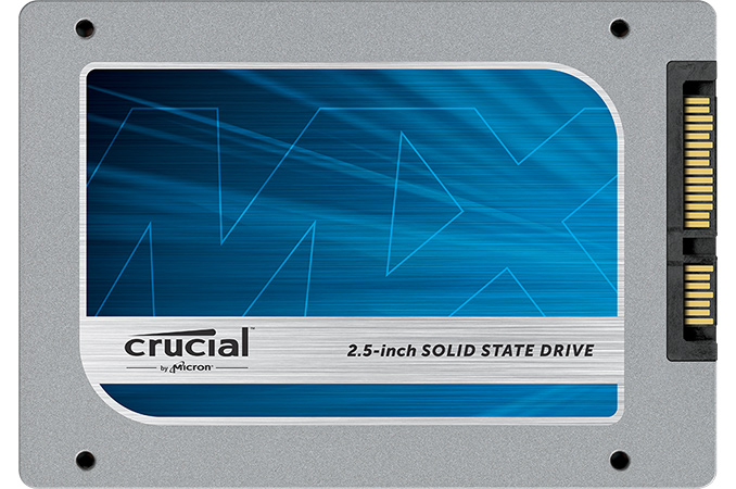
The Crucial MX300 SSDs are based on the company’s first-generation 32-layer 3D TLC NAND as well as Marvell’s 88SS1074 controller. Just like other MX-series drives, the new devices fully support encryption, pseudo-SLC caching for faster writes, partial power loss protection and a three-year warranty. We reviewed the 750GB version of the MX300 earlier this year, and you can read the review here.
Due to the 384 Gb (48 GB) capacity of Micron’s 3D TLC NAND, the configurations of actual SSDs seem somewhat unusual, but Micron has stated this does not affect performance or endurance of the novelties. According to the manufacturer, the MX300 drives support sequential read performance up to 530 MB/s as well as sequential write performance up to 510 MB/s (which is in line with affordable TLC NAND-based drives). The SSDs are also rated for up to 92K/83K random read/write IOPS.
Crucial MX300 Series Specifications Capacity MX300
275 GBMX300
525 GBMX300
750GBMX300
1 TBMX300
2 TBForm Factors 2.5", M.2 2.5" 2.5", M.2 2.5" Controller Marvell 88SS1074 NAND Micron 384 Gbit 32-layer 3D TLC DRAM unknown 512 MB unknown Seq Read 530 MB/s Seq Write 500 MB/s 510 MB/s 4K Rand Read 55K IOPS 92K IOPS 4K Rand Write 83K IOPS DevSleep 4mW Slumber Power 75mW Max Power unknown 5.2W unknown Encryption TCG Opal 2.0 & IEEE-1667 (eDrive) Endurance 80 TB 160 TB 220 TB 360 TB 400 TB Warranty Three years Price (2.5") $69.99 $129.99 $189.99 $259.99 unknown Back in April, Crucial introduced its limited edition MX300 750 GB SSD (which we reviewed) and this week it expanded the family with 275 GB, 525 GB as well as 1 TB models to address different segments of the market. The currently available Crucial MX300 drives come in a 2.5”/7mm form-factor with a SATA interface, with an M.2 version coming later in August for the 275 GB/525 GB/1 TB models. A good news is that the forthcoming MX300 M.2 drives promise to deliver the same performance and endurance as the 2.5-inch drives.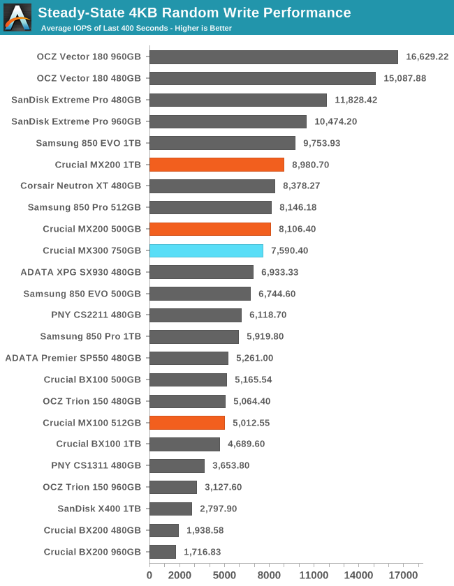

As for pricing, the 275 GB, 525 GB, 750 GB and 1TB 2.5-inch versions of the MX300 from Crucial will be available for MSRP of $69.99, $129.99, $189.99 and $259.99 respectively (note that the 750 GB version is $10 cheaper than launch). Prices of the MX300 M.2 drives, as well as MX300 2 TB SSDs, are not set yet.
More...


 Quote
QuoteThread Information
Users Browsing this Thread
There are currently 42 users browsing this thread. (0 members and 42 guests)


Bookmarks