

Results 6,221 to 6,230 of 12096
Thread: Anandtech News
-
08-18-16, 08:16 AM #6221
Anandtech: HP and MAINGEAR Team Up for Omen X High-End Gaming PC
HP this week re-entered the market of high-end gaming PCs with its Omen X desktop. The machine uses rather unusual cube-shaped tri-chamber design featuring high-end hardware, liquid cooling and various upgrade options. HP will offer customized versions of the Omen X, but MAINGEAR will sell something more exclusive with additional customization options, Intel Core i7 Extreme CPUs, hand-build liquid cooling as well as factory overclocking.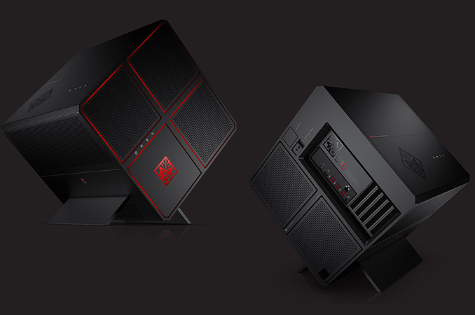
The year was 2006. PC gaming was not particularly on the rise (and the word eSports was non-existent), but the interest towards high-end PC gaming technologies was high, particularly because the demographics of gamers got older and more of those people could afford ultra-high-end gaming computers as well as components. This is when Dell acquired Alienware and HP bought Voodoo PC in a bid to address the growing and lucrative segment of the PC market. While the two large PC makers made a similar decision and bought leading boutique PC makers, there actions afterwards were substantially different. While both tried to integrate their gaming PC subsidiaries, Dell has succeeded and made Alienware its integral part of itself, whereas HP first ceased to sell expensive custom desktops, then started to place VoodooDNA brand on various high-end machines and then stopped building PCs for any demanding gamers at all. Apparently, HP was not interested in serving a relatively small segment of the PC market after multiple enterprise-oriented acquisitions. However, now that HP’s consumer business is a separate company, the latter seems to be gaining interest towards high-end machines, which is why it unveiled its Omen X system. Nonetheless, the company does not plan to address the market of boutique PCs just now, which is why it teamed up with MAINGEAR for advanced versions of the Omen X. While HP does not use the Voodoo brand for its Omen X, its machine carries the distinctive logotype on it.
The cube-shaped 45° angled design of the Omen X is meant to simplify access to hardware by the end-user. While the form of the Omen X is very distinctive, its concept is very similar to other modern desktops. The chassis sports three chambers to separate hot components (CPU+GPU, hard drives and PSU) from each other and optimally cool-down each chamber/set of components. The Omen X chassis can fit it one Micro-ATX motherboard (with one M.2 slot, two PCIe x16 slots, four DDR4 slots and so on), two graphics cards, two 3.5” storage devices/three 2.5” SSDs/HDDs, one M.2 SSD, one ODD, and one high-end PSU, with MAINGEAR offering up to a 1200 W Corsair AX1200i model.
While architecturally the HP Omen X and the MAINGEAR Omen X are exactly the same, there are substantial differences when it comes to their configurations, which is why we basically talking about two rather different systems here. HP only offers Intel’s LGA1151 processors as well as up to two AMD Radeon R9 Fury X or NVIDIA GeForce GTX 1080 graphics cards with its Omen X. By contrast, MAINGEAR offers only LGA2011-3 platforms, up to ten-core Core i7-6950X CPU, up to two NVIDIA Titan X (Pascal) graphics cards, hand-made liquid cooling as well as custom exterior finish with automotive paint. The differences of configurations naturally affect prices: the HP Omen X starts at $1800, whereas MAINGEAR-built Omen X starts at $3000 with more advanced “superstock” version available for $5200.
All Omen X systems use industry-standard components, so it will be possible for owners to upgrade them as they wish (subject to terms and conditions of warranty) using any aftermarket part. Still, keeping in mind that MAINGEAR offers custom liquid cooling solutions, it may not be that easy to upgrade such machines without re-building the LCS.Specifications of HP and MAINGEAR Omen X Desktops HP Omen X MAINGEAR Omen X CPU Intel Core i5/i7 Skylake-S
Up to Intel Core i7-6700KIntel Core i7 Extreme Broadwell-E
Up to Intel Core i7-6950XPCH Intel Z170 Intel X99 Motherboard HP custom ASUS X99-M WS Graphics Up to two AMD Radeon R9 Fury X or NVIDIA GeForce GTX 1080 Up to two NVIDIA Titan X
No AMD Radeon optionsCooling Air cooling
Optional closed-loop liquid cooling with 120 mm radiatorsIntel retail CPU cooler
Closed Loop — EPIC 240 MAINGEAR CPU SuperCooler
Regular Open Loop — Custom liquid cooling for CPU and GPU with 360mm radiator and high airflow fans
Superstock Open Loop — Custom hand crafted liquid cooling with crystal hardline or metal hardline tubing, premium Chrome fittings, 360mm copper core radiators and high airflow fansMemory Four DIMM slots, up to 64 GB of DDR4-3000 M.2 One M.2 (PCIe 3.0 x4) slot for up to 2280 SSDs SATA connectors 3 3 (actual motherboard has 8) SATAe connectors unknown 1 (only available in single-GPU systems) eSATA connectors 0 0 Storage bays 2x3.5"
3x2.5"
1x5.25" (for portable ODDs)Wi-Fi unknown 802.11ac + BT 4.0 Ethernet Gigabit Ethernet Gigabit Ethernet based on either
Intel I218V GbE or
Intel I211AT GbEDisplay Outputs HDMI/DP/DVI - according to GPU specs + one HDMI on the motherboard HDMI/DP/DVI - according to GPU specs Audio HDMI
Optical S/PDIF
a mini-jack for headphones
a mini-jack for microphoneFive 7.1-channel audio connectors
a mini-jack for headphones
a mini-jack for microphone
Optcal S/PDIFUSB 8 x USB 3.0 Type-A
2 x USB 3.0 Type-C with fast charging2 x USB 3.1 Type-A (10 Gbps, ASMedia ASM1142)
6 x USB 3.0 Type-ADimensions 20" (H) x 16" (W) x 20" (D)
50.8 cm (H) x 40.6 cm (W) x 50.8 cm (D)PSU 600 W ~ 1300 W PSUs by HP 750 W EVGA SuperNOVA 80 Plus
860 W Corsair PAX860 80+ Platinum
1200 W Corsair AX1200i 80+ PlatinumVisual Aesthetics Custom lighting:
- Nine lighting zones
- Four color modesChassis lighting
Custom exterior finish with automotive Glasurit paints
HP plans to start shipments of its Omen X at a later date, whereas MAINGEAR intends to ship its Omen X in mid-September.
In addition to Omen X desktops, HP also plans to offer a complimentary set of Omen-branded peripherals (with Voodoo logotype on them). The initial family will include a headset and a mouse designed by SteelSeries as well as a 32” display.
Sources: HP, MAINGEAR.
Gallery: HP and MAINGEAR Team Up for Omen X High-End Gaming PC


More...
-
08-18-16, 05:31 PM #6222
Anandtech: NVIDIA Releases GeForce GTX 1060 3GB: GTX 1060, Yet Not
In a low-key press blast sent today, NVIDIA has announced that they are expanding the GeForce 10-Series of cards with another entry. Augmenting the current series of cards is a second GeForce GTX 1060, the GeForce GTX 1060 3GB, which despite the name is not actually equal to the original, 6GB GeForce GTX 1060. The new GTX 1060 3GB is available immediately from retailers starting at $199.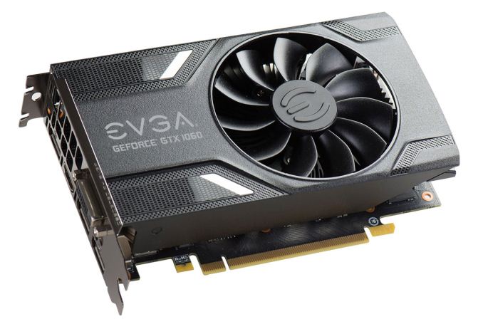
Looking at the big picture, the new GTX 1060 3GB materially differs from the existing 6GB GTX 1060 in two different metrics. First and foremost of course is the memory; the card ships with half as much memory, which amounts to a 6x512MB configuration. However, somewhat frustratingly, NVIDIA didn’t just stop there and has also introduced a new GPU configuration for this card, meaning that we are now looking at multiple GPU configurations being sold at retail under the GTX 1060 banner.NVIDIA GPU Specification Comparison GTX 1070 GTX 1060 6GB GTX 1060 3GB GTX 960 CUDA Cores 1920 1280 1152 1024 Texture Units 120 80 72 64 ROPs 64 48 48 32 Core Clock 1506MHz 1506MHz 1506MHz 1126MHz Boost Clock 1683MHz 1709MHz 1709MHz 1178MHz TFLOPs (FMA) 6.5 TFLOPs 4.4 TFLOPs 3.9 TFLOPs 2.4 TFLOPs Memory Clock 8Gbps GDDR5 8Gbps GDDR5 8Gbps GDDR5 7Gbps GDDR5 Memory Bus Width 256-bit 192-bit 192-bit 128-bit VRAM 8GB 6GB 3GB 2GB FP64 1/32 1/32 1/32 1/32 TDP 150W 120W 120W 120W GPU GP104 GP106 GP106 GM204 Transistor Count 7.2B 4.4B 4.4B 2.94B Manufacturing Process TSMC 16nm TSMC 16nm TSMC 16nm TSMC 28nm Launch Date 06/10/2016 07/19/2016 08/18/2016 01/22/2015 Launch Price MSRP: $379
Founders $449MSRP: $249
Founders $299MSRP: $199 $199
Whereas the original GTX 1060 6GB shipped with a fully enabled GP106 GPU, the GPU used in the GTX 1060 3GB ships with 1 of the 10 SMs enabled. This leaves 9 SMs enabled, leading to a CUDA core count of 1152, and 72 texture units. Other than this sole disabled SM, the GPU is otherwise untouched, and the full ROP/L2 backend and its associated memory controllers are fully enabled.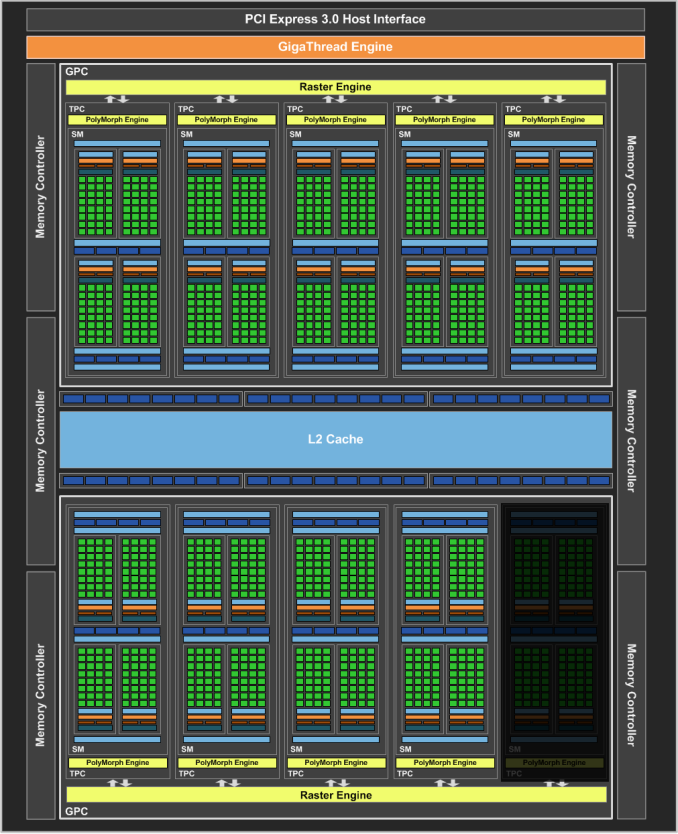
Clockspeeds are also unchanged. On the GPU this means we’re still looking at 1506MHz base and 1709MHz boost. Meanwhile on the memory it’s still 8Gbps GDDR5 on a 192-bit memory bus, only now there’s only half as much total memory. Consequently the total performance hit to the GTX 1060 3GB as compared to the original GTX 1060 6GB will be a combination of the reduced memory capacity and the loss of 10% of the shading/texturing/geometry resources.
Finally, on the TDP side, TDP hasn’t been adjusted even with the loss of 1 SM. This means TDP remains at 120W. I suspect part of this comes down to the fact that NVIDIA isn’t doing additional power binning (ala GTX 1070), along with the fact that disabling a single SM is going to have a limited impact on power consumption.
All told, this is a typical case of NVIDIA creating a new SKU for salvaged GPUs. Since the full-fledged GTX 1060 uses an equally full-fledged GP106, this gives salvaged GP106s a card to use them in.
The concern I have is that, frankly, I thought NVIDIA was done with these shenanigans, as they haven’t had multiple GPU configurations selling under a single retail GTX model number for a number of years now. To the company’s credit, they are drawing a clear line between the 3GB and 6GB cards – there will not be any 6GB cards with a cut-down GPU, nor any 3GB cards with the full GPU – but the memory configuration now means something about how the GPU is configured, which is unintuitive at best (ed: and this doesn’t give AMD a free pass on the RX 480 either). Ultimately I’m not sure that anything good can come from this, and that the part should have been GTX 1055 or such.
Meanwhile the performance impact, according to NVIDIA, should be about 5%. Keeping in mind that GTX 1060 3GB is losing 10% of its shader/texture/geometry capacity and none of its ROP or rasterization capacity, this doesn’t seem unrealistic. Though it’s obviously something we’ll want to test ourselves.
As mentioned earlier, this is a hard launch for NVIDIA and its partners. MSI, Gigabyte, EVGA, and others are already listing cards on Newegg, and as of this afternoon they are still in stock, which is better than any previous 10-Series launch. Even the base-bones $199 GTX 1060 3GB cards are in stock, so it’s possible to pick up a card at MSRP. Though the partners also have a number of factory overclocked cards, in case you wish to spend more than $200.
Competitively speaking, the GTX 1060 3GB is meant to compete against the $199 4GB Radeon RX480, the cheaper of AMD’s RX 480 lineup. The latter has been in very short supply since its launch, so at this second NVIDIA has a pretty solid grip on the $199 price point at this secnd.
At the same time however, I do have some concerns about whether a 3GB card is enough, especially looking at a year or so down the line. The 2GB GTX 960, by comparison, has shown us that buying a low capacity card can be short-sighted, as the 4GB versions have held up better in 2016’s major game releases. But to the credit of NVIDIA and their partners here, they are at least being aggressive on pricing, with the slight downgrade from the 6GB to the 3GB card shaving 20% ($50) off of the MSRP of the card.
Finally, on a housekeeping note, NVIDIA has not sampled the 3GB cards to the press, as this is a pure virtual (partner-driven) launch with no reference board or Founders Edition equivalent. So you’ll see reviews over the coming days and weeks as partners directly sample cards instead.
Summer 2016 GPU Pricing Comparison AMD Price NVIDIA $439 GeForce GTX 1070 Radeon R9 390X $329 Radeon R9 390 $299 $249 GeForce GTX 1060 6GB Radeon RX 480 (8GB) $239 Radeon RX 480 (4GB)
Radeon RX 470$199 GeForce GTX 1060 3GB
More...
-
08-18-16, 11:00 PM #6223
Anandtech: Early AMD Zen Server CPU and Motherboard Details: Codename Naples, 32-co
At the AMD Zen microarchitecture announcement event yesterday, the lid was lifted on some of the details of AMD’s server platform. The 32-core CPU, codename Naples, will feature simultaneous multithreading similar to the desktop platform we wrote about earlier, allowing for 64 threads per processor. Thus, in a dual socket system, up to 128 threads will be available. These development systems are currently in the hands of select AMD partners for qualification and development.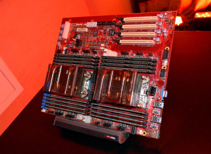
AMD was clear that we will expect to hear more over the coming months (SuperComputing 2016 is in November 2016, International SuperComputing is in June 2017) with a current schedule to start providing servers in Q2 2017.
Analysing AMD’s 2P Motherboard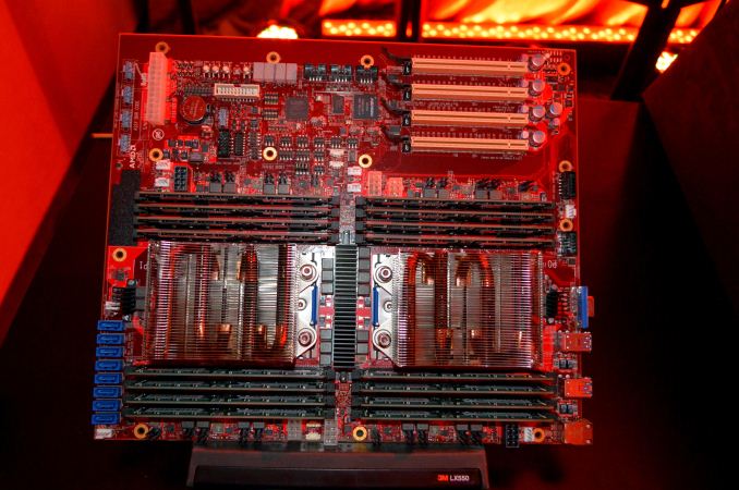
AMD showed off a dual socket development motherboard, with two large AMD sockets using eight phase power for each socket as well as eight DDR4 memory slots.
It was not stated if the CPUs supported quad-channel memory at two DIMMs per channel or eight channel memory at this time, and there’s nothing written on the motherboard to indicate which is the case – typically the second DIMM slot in a 2DPC environment is a different color, which would suggest that this is an eight-channel design, however that is not always the case as some motherboard designs use the same color anyway.
However, it is worth noting that each bank of four memory slots on each side of each CPU has four chokes and four heatsinks (probably VRMs) in two sets. Typically we see one per channel (or one per solution), but the fact that each socket seems to have eight VRMs for the memory would also lean into the eight-channel idea. To top it off, each socket has a black EPS 12V (most likely for the CPU), which is isolated and clearly for CPU power, but also a transparent EPS 12V and a transparent 6-pin PCIe connector. These transparent connectors are not as isolated, so are not for low power implementation, but each socket does have one attached, perhaps suggesting that the memory interfaces are powered independently to the CPU. More memory channels would require more power, and four-channel interfaces have been done and dusted before via the single EPS 12V, so requiring even more power raises questions. I have had word in my ear that this may be as a result of support for future high energy memory, such as NVDIMM, although I have not been able to confirm this.
Unfortunately, we could not remove the heatsinks to see the CPUs or the socket, but chances are this demo system would not have CPUs equipped in the first place. Doing some basic math based on the length of a DDR4 module, our calculations show that the socket area (as delineated by the white line beyond the socket) is 7.46 cm x 11.877 cm, to give an area of 88.59 cm2. By comparison, the heatsink has an active fin floor plan area of 62.6 cm2 based on what we can measure. Unfortuantely this gives us no indication of package area or die area, both of which would be more exciting numbers to have.
Putting the CPU, memory and sockets aside, the motherboard has a number of features worth pointing out. There is no obvious chipset or southbridge in play here. Where we would normally expect a chipset, we have a Xilinx Spartan FPGA without a heatsink, although I would doubt this is the chipset based on the fact that there is an ‘FPGA Button’ right above it and this is most likely to aid in some of the debugging elements on the system.
Further to this, the storage options for the motherboard are all located on the left hand side (as seen) right next to one of the CPUs. Eight SATA style ports are here, all in blue which usually indicates that these are part of the same head controller, but also part of the text on the motherboard states ‘ALL SATA CONNS CONNECTED TO P1’ which indicates the first processor has direct control.
Other typical IO on the rear panel such as a 10/100 network port (for the management) and the USB 3.0 ports are next to the second processor, which might indicate that this processor has IO control over these parts of the system. However the onboard management control, provided by an ASpeed AST2500 controller with access to Elpida memory, is nearer the PCIe slots and the Xilinx FPGA.
The lack of an obvious chipset, and the location of the SATA ports, would point to Naples having the southbridge integrated on die, and creating an SoC rather than a pure CPU. Bringing this on die, to 14nm FinFET, will allow the functions to be in a lower power process (historically chipsets are created at a larger lithography node to the CPU) as well as adjustments in bandwidth and utility, although at the expense of modularity and die area. If Naples has an integrated chipset, it makes some of the findings on the AM4 platform we saw at the show very interesting. Either that or the FPGA is actually used for the developers to change southbridge operation on the fly (or that chipsets are actually becoming more like FPGAs, which is more realistic as chipsets move to PCIe switch mechanisms).
There are a lot of headers and jumpers on board which won’t be of much interest to anyone except the platform testing, but the PCIe layout needs a look. On this board we have four PCIe slots below one of the CPUs, each using a 16 lane PCIe slot. By careful inspection of the pins we can certainly tell that the slots are each x16 electrical.

However the highlighted box gives some insight into the PCIe lane allocation. The text says:
“Slot 3 has X15 PCIe lanes if MGMT PCIe Connected
Slot 3 has X16 PCIe lanes if MGMT PCIe Disconnected”
This would indicate that slot three has a full x16 lane connection for data, or in effect we have 64 lanes of PCIe bandwidth in the PCIe slots. That’s about as far as we can determine here – we have seen motherboards in the past that take PCIe lanes from both CPUs, so at best we can say that in this configuration that the Naples CPU has between 32 lanes and 64 lanes for a dual processor system. The board traces, as far as we were able to look at the motherboard, did not make this clear, especially when this is a multi-layer motherboard (qualification samples are typically over-engineered anyway). There is an outside chance that the integrated southbridge/IO is able to supply an x16 combination PCIe lane, however there is no obvious way to determine if this is the case (and is not something we’ve seen historically).
AM4 Desktop Motherboards
Elsewhere on display for Zen, we also saw some of the internal AM4 motherboards in the base units at the event.
These were not typical motherboard manufacturer boards from the usual names like ASUS or GIGABYTE, and were very clearly internal use products. We weren’t able to open up the cases to see the boards better, but on closer inspection we saw a number of things.
First, there were two different models of motherboards on show, both ATX but varying a little in the functionality. One of the boards had twelve SATA ports, some of which were in very odd locations and colors, but we were unable to determine if any controllers were on board.
Second, each of the boards had video outputs. This would be because we already know that the AM4 platform has to cater for both Bristol Ridge and Summit Ridge, with the former being APU based with integrated graphics and the updated Excavator v2 core design. On one of the motherboards we saw two HDMI outputs and a DisplayPort output, suggesting a full 3-digital display pipeline for Bristol Ridge.
The motherboards were running 2x8GB of Micron memory, running at DDR4-2400. Also, the CPU coolers – AMD was using both its 125W AMD Wraith cooler as well as the new 95W near silent cooler between all four/five systems on display. This pegs these engineering samples at a top end of this TDP, but if recent APU and FX product announcements are anything to go by, AMD is happy to put a 125W cooler on a 95W CPU, or a 95W cooler on a 65W CPU if required.
I will say one thing that has me confused a little. AMD has been very quiet on the chipset support for AM4, and what IO the south bridge will have on the new platform (and if that changes if a Bristol or Summit Ridge CPU is in play at the time). In the server platform, we concluded above that the chipset is likely integrated into the CPU – if that is true on the consumer platform as well, then I would point to the chipset-looking device on these motherboards and start asking questions. Typically the chipset on a motherboard is cooled by a passive heatsink, but these chips here had low z-height on fans them and were running at quite the rate. I wonder if they were like this so when the engineers use the motherboards it means there is more space to plug testing tools, or if it for another purpose entirely. As expected, AMD said to expect more information closer to launch.
Wrap Up
To anyone who says motherboards are boring, well I think AMD has given a number of potential aspects of the platform away in merely showing a pair of these products for server and desktop. Sure, they answer some questions and cause a lot more of my hair to fall out trying to answer the questions that arise, but at this point it means we can start to have a fuller understanding of what is going on beyond the CPU.
As for server based Zen, Naples, depending on PCIe counts and memory support, along with the cache hierarchy we discussed in the previous piece, the prospect of it playing an active spot in enterprise seems very real. Unfortunately, it is still a year away from launch. There are lots of questions about how the server parts will be different, and how the 32-cores on the SKUs that were talked about will be arranged in order to shuffle memory around at a reasonable rate – one of the problems with large core count parts is being able to feed the beast. AMD even used that term in their presentation, meaning that it’s clearly a topic they believe they have addressed.
Gallery: Early AMD Zen Server CPU and Motherboard Details: Codename Naples, 32-cores, Dual Socket Platforms, Q2 2017


More...
-
08-22-16, 04:18 AM #6224
Anandtech: ARM Announces ARM v8-A with Scalable Vector Extensions: Aiming for HPC and
Today ARM is announcing an update to their line of architecture license products. With the goal of moving ARM more into the server, the data center, and high-performance computing, the new license add-on tackles a fundamental data center and HPC issue: vector compute. ARM v8-A with Scalable Vector Extensions won’t be part of any ARM microarchitecture license today, but for the semiconductor companies that build their own cores with the instruction set, this could see ARM move up into the HPC markets. Fujitsu is the first public licensee on board, with plans to include ARM v8-A cores with SVE in the Post-K RIKEN supercomputer in 2020.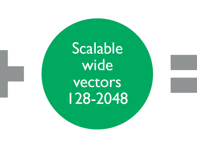
Scalable Vector Extensions (SVE) will be a flexible addition to the ISA, and support from 128-bit to 2048-bit. ARM has included the extensions in a way that if included in the hardware, the hardware is scalable: it doesn’t matter if the code being run calls for 128-bit, 512-bit or 2048-bit, the scheduler will arrange the calculations to compensate for the hardware that is available. Thus a 2048-bit code run on a 128-bit SVE core will manage the instructions in such a way to complete the calculation, or a 128-bit code on a 2048-bit core will attempt to improve IPC by bundling 128-bit calculations together. ARM’s purpose here is to move the vector calculation problem away from software and into hardware.
This is different to NEON, which works on 64-bit and 128-bit vectors. ARM is soon submitting patches to GCC and LLVM to support the auto-vectorization for VSE, either by directives or detecting applicable command sequences.
Performance metrics performed in ARMs labs show significant speed up for certain data sets already and expect that over time more code paths will be able to take advantage of SVE. ARM is encouraging semiconductor architecture licensees that need fine-grained HPC control to adopt SVE in both hardware and code such that as the nature of the platform adapts over time both sides will see a benefit as the instructions are scalable.
Gallery: ARM Announces ARM v8-A with Scalable Vector Extensions: Aiming for HPC and Data Center


More...
-
08-22-16, 08:21 AM #6225
Anandtech: The Tesoro Gram Spectrum Low Profile Mechanical Keyboard Review
Today we are taking our first look at a “low-profile” mechanical keyboard, the Tesoro Gram Spectrum. The Gram Spectrum features RGB lighting and full programmability, but its highlight are the new Kailh Agile switches and low profile keycaps, which significantly reduce the overall key height and travel.
More...
-
08-22-16, 03:00 PM #6226
Anandtech: Android 7.0 Nougat Released
Google has completed its five month beta program and is officially releasing Android 7.0 Nougat today. The company will begin rolling it out to select Nexus devices, including the Nexus 5X, Nexus 6P, Nexus 6, Nexus 9, Nexus Player, the Pixel C tablet, and the General Mobile 4G (Android One phone), as an OTA over the next few weeks. The Nexus 5 and 7 (2013) are not eligible for the update.
The LG V20 will be the first new device to ship with Nougat installed. Manufacturers and carriers have not committed to a specific timeline for rolling out updates for existing devices, however. Samsung’s President of Mobile, Koh Dong-jin, revealed in an interview with The Korea Times that the recently released Galaxy Note7 should receive an update perhaps in the next 2-3 months. HTC stated that the HTC 10, HTC One A9, and HTC One M9 will all be receiving Nougat updates, but did not provide any dates, only stating that timing and any additional eligible devices will be announced later.
We took our first look at some of Nougat’s features when we got our hands on the first developer beta back in March. Since then, Google has continued to refine the OS and add new features. The new Split-Screen mode, which provides a native API for using two apps side by side, should provide a boost for multitasking. This will be more useful for tablets, but phablet phones should benefit too. There’s also many smaller tweaks, such as double-tapping the overview button to switch between the two most recently used apps, that improve usability and productivity.
Nougat also includes the ability for apps to bundle notifications, reducing clutter on the lock screen or in the notification shade. The bundles can be expanded for more detailed information about each specific notification, and you can even reply to notifications directly from the notification shade without launching an app first.
Performance and battery life should also improve with Nougat. The updated JIT compiler claims to improve the runtime performance of apps while also reducing the amount of storage space they require. Android 7.0 also includes official support for the new Vulkan graphics API. Similar to Apple’s Metal, it’s a low-level API that dramatically improves 3D performance by reducing the overhead of draw calls. The changes to Android’s Doze feature, first introduced in Android Marshmallow, promise a small boost to battery life by allowing the phone to go into a lower power state when it’s being carried around with the screen locked.
Android has been plagued with security issues, and while this will remain a topic of concern for the foreseeable future, Nougat does bring some new security enhancements. Perhaps the biggest change is the hardening of Android’s Stagefright mediaserver library—a combination of better code sanitization to eliminate buffer overflows and splitting the library into several sandboxed components with more restricted permissions. Nougat also adds file-based encryption, a more secure boot process, and behind-the-scenes OS updates.
Nougat provides too many improvements to fully cover here, but even the visible and not so visible changes mentioned above should prove to be welcome additions to Android.
More...
-
08-23-16, 12:02 AM #6227
Anandtech: Hot Chips 2016: NVIDIA Pascal GP100 Die Shot Released
The first day of conference sessions wrapped up earlier this evening at the annual Hot Chips symposium. One of the computing industry’s lower-key events, the IEEE conference for high performance chips is not a venue for product announcements, but instead a more focused conference for tech companies and their engineers to let their hair down a bit and present some deeper technical workings of their products. Even these aren’t full product briefings – since they’re often for future products – but it’s a good venue to dive a little deeper and learn a little bit more about the technologies and decisions that have gone into putting these chips together.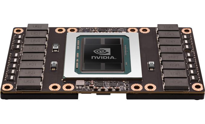
Over the next two days we’ll be covering the highlights of several presentations, but I wanted to start this year’s coverage off with some nerdy pictures. I am of course referring to die shots, as NVIDIA has released the first die shot of their behemoth 610mm2 GP100 die as part of a presentation on Pascal and NVLink 1.0. Die shots have been relatively rare in the GPU industry in recent years, particularly those for the highest-end GPUs with the most features.
GP100 is particularly interesting because it’s the first NVIDIA part featuring HBM and NVLink, two interfaces which (at least for NVIDIA) premiered on GP100. The die shot itself is not significantly enhanced (and I’m not going to spoil a good die shot here), but even with just basic coloring you can make out features such as the thread scheduler and other uncore features in the center, along of course with the SMs. GP100, as a reminder, has 60 in all, organized into 30 TPCs, the latter of which is what you’re probably counting right now.
Top and bottom of this picture appear to be the HBM2 interfaces. Despite the width of GP100’s 4096-bit HBM2 bus, the space consumed by HBM2 appears to be relatively small on the admittedly large GPU, which is one of the benefits of HBM as it allows for very tight routing and simpler GPU-side logic. Going HBM didn’t just get NVIDIA more memory bandwidth, but I fully expect it also got them a meaningful increase in die area that they could dedicate to GPU logic.
Meanwhile the presentation also gives us our best shot to date of a full (and presumably production) GP100 package. Note the tight spacing between the HBM2 stacks and the GPU die; NVIDIA did not waste any space here, as the memory stacks have been placed as close as they can be. Both the memory and GPU sit on top of the silicon interposer, itself not much larger than the hardware it sits on. Due to the large size of GP100, every millimeter ends up mattering here, as the resulting interposer has to be quite large even with this dense packing. This also does a great job illustrating just how much larger HBM2 stacks are than HBM1 stacks, as they now are a considerable fraction of the die size of GP100 itself, as opposed to the smaller HBM1 stacks used on AMD's Fury X last year.
The big question, of course, is when this technology will trickle down into cheaper, consumer-level boards. Right now HBM2 is still quite expensive, while GDDR5X has allowed NVIDIA to cover much of their bandwidth needs on consumer parts with the cheaper memory technology. However as we’ll see in the Hot Chips memory presentation, Samsung and Xilinx have some ideas on how to handle that…
More...
-
08-23-16, 02:14 AM #6228
Anandtech: Hot Chips 2016: Memory Vendors Discuss Ideas for Future Memory Tech - DDR5
Continuing our Hot Chips 2016 coverage for the evening, along with the requisite presentations on processors, several of the major players in the memory industry are also at the event making their own presentations. A fast chip is only as swift as the memory that is responsible for feeding it, so the development of faster processors is inexorably tied to the development of faster memory technologies and the introduction of additional layers to the computer memory hierarchy.
Like the chip presentations themselves, I should be clear that these aren’t product announcements. But they’re a short, useful look into the challenges the memory manufacturers face and what ideas they’re floating for future generations of memory technology.
Micron
The first memory manufacturer to present was Micron. The firm has an interesting stake in the memory industry; while producing a number of common adopted memory technologies like DDR3 and DDR4, they have also gone their own way in pioneering HBM competitor Hybrid Memory Cube (HMC) and the faster GDDR5X memory technology. The former has not seen much success so far, while the latter has been adopted by NVIDIA for their highest bandwidth configurations on consumer (non-GP100) parts.
One interesting slide from Micron’s presentation was showing how the memory industry has been impacted by the greater difficultly in manufacturing at smaller geometries. The number of mask levels has increased over the years – especially the number of non-lithographic steps within those mask levels – and meanwhile the total amount of cleanroom space required to hold all of the necessary equipment has similarly increased as well. For an equivalent number of wafers, Micron’s 20nm tech takes more than 80% additional space compared to 30nm, which is not very far off from the 100% increase in memory density that you get from going from 30nm to 20nm in the first place.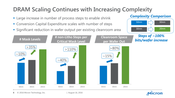
The lesson here being that memory manufacturers are facing many of the same constraints as logic manufacturers. Every generation the capital costs increase – and significantly at that – which squeezes margins and investors alike. The memory industry has seen a fairly regular pattern of boom and bust cycles up until now, with each bust cycle claiming a manufacturer or two. However as the number of manufacturers dwindle, I’m not sure consolidation alone is going to be able to continue to offset the higher costs.
Meanwhile turning towards the future, the company very briefly mentioned their current plan for the memory technology that will follow DDR4, which is aptly being named DDR5. Keeping in mind that the standard has yet to be created and ratified by the JEDEC – and likely won’t be for a couple more years – Micron would essentially like to once again double the DRAM prefetch yet again, to 16n (the same as GDDR5X). Doubling the prefetch doesn’t increase the memory’s internal clock rate, but allows for a larger number of bits to be gathered per clock, and sent out over the higher frequency bus. All the while Micron would also like to get the memory voltage down to 1.1v from today’s 1.2v for standard DDR4.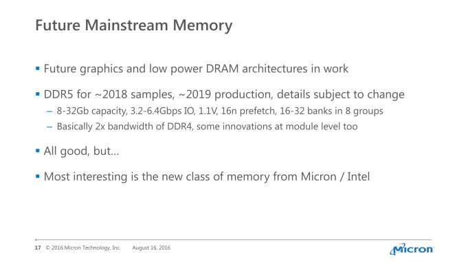
Presumably this would be using a form of QDR (like GDDR5X), with the current aim to get it into production in 2019.
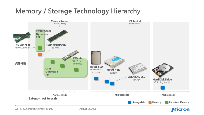 Finally, Micron also published a useful slide that helps to illustrate where they see 3D XPoint memory fitting into the computer memory hierarchy. This is essentially split between SSD-style implementations that access the memory over the PCIe bus, and RAM-style implementations that access the memory over standard memory buses in the form of DIMMs. Neither is as fast as DRAM (and 3D XPoint lacks the near-infinite endurance of DRAM), but it allows for interesting concepts such as databases stored almost entirely in 3D XPoint memory in DIMM form, allowing for relatively fast access combined with the inherent non-volatility of the memory.
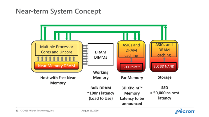
Samsung
The second of the memory manufacturers to present was Samsung. Compared to Micron, Samsung has walked the more traditional path, embracing HBM and opting not to build GDDR5X. As a result, in their presentation looking at future memory technologies, we’re seeing where they want to go from today’s HBM2 and GDDR5 technologies.
Throughout their presentation, Samsung laid out ideas for new generation memory standards for DDR, LPDDR, and GDDR5. The bulk of Samsung’s material was on the latter two, focusing their efforts on the realms of high-bandwidth memory technologies and low-power memory technologies.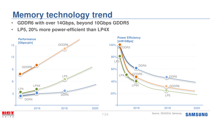
On the low-power side, Samsung is proposing a technology they are calling LP(DDR)4X. An extension of current LPDDR4, Samsung wants to enact changes that allow reducing the memory bus voltage (VDDQ) from 1.1v to 0.6v, nearly halving the voltage required. The end goal would be to further reduce the power consumption of I/O – so not the memory itself, but rather moving data around – which combined with a process node shrink Samsung estimates could reduce total DRAM power consumption by 18%.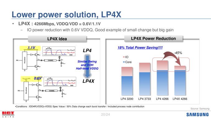
As for why Samsung would do this, one needs to look no further than mobile. Power is the ultimate limiting factor of computing performance these days, and that is especially the case on mobile where there is a fixed heat budget and a fixed total power budget in joules. So any reduction in power consumption can either extend battery life, or allow Samsung to further ramp up memory performance at the same power level.
The company also floated some high-level ideas for where they’d like to go with Post LP4 (LPDDR5). Through some optimizations such as even deeper sleep states and adjustments to factors like the precharge standby current, Samsung would like to reduce power consumption per Gbps a further 20% over LP4X.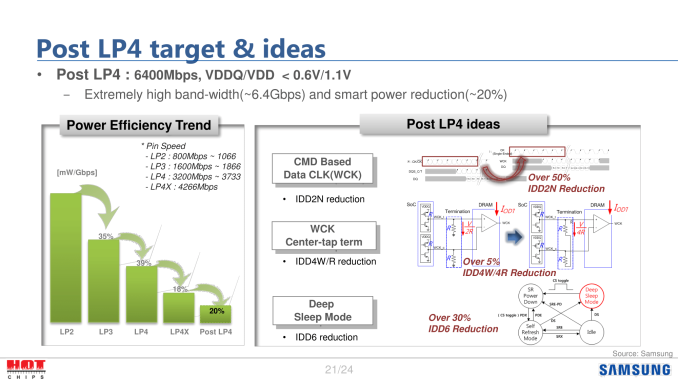
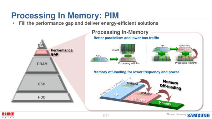 One other idea the company is floating particularly for SoC-type designs is PIM – Processing In Memory. This would move some logic into the DRAM, allowing processing to take place closer to the memory source. The impetus behind this is that I/O power remains one of the biggest components of memory power consumption, and in theory it’s unnecessary since it’s simply moving data rather than processing it or load/storing it. The concept here then would be that by moving some processing closer to DRAM – say parts of a GPU – then less power is spent sending data to the GPU over the expensive memory bus. Instead what’s sent is the already processed data, which is a smaller amount of data, and consequently takes less power to send. The risk, of course, is that you’re now mixing logic with memory, which can be harder to implement and validate.
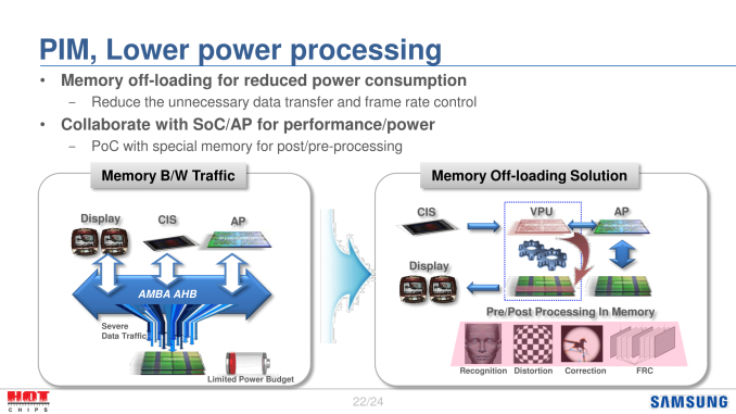
Curiously, Samsung is going almost the opposite direction at the high-end of the memory market. In a proposal for low-cost HBM, Samsung laid out a plan for how to bring down the complexity of HBM, and as a result the total cost of the fast-but-expensive memory technology. The low cost proposal essentially trades off some width for frequency; moving a stack from 1024-bits to 512-bits, but increasing the per-pin frequency by 50%. The net result is still less bandwidth than HBM2, but not immensely so.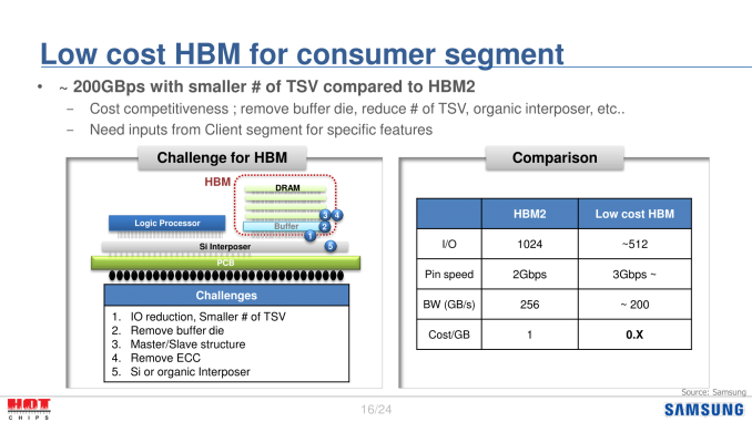
The big savings here come from the narrower width allowing for simpler memory stacks with fewer TSVs. TSVs are the breakthrough technology that make HBM possible, but they also remain one of the most stubborn components to get correct, as thousands of vias must be wired up inside a single stack. So a die stack with fewer TSVs will be easier to manufacturer.
The other interesting aspect of this proposal is that Samsung wants to remove the base logic/buffer die. To be honest I’m not 100% sure how this would work, as one of the fundamental tenants of HBM is that it’s a logic-to-logic (processor to logic die) connection, with the HBM stack’s logic die then coordinating the relatively dumb DRAM layers. Removing the logic die would certainly bring down costs, as it means no longer meshing logic with DRAM on a single package, but it’s not clear where the HBM PHY lies on the cost-reduced memory stack.
Finally, partially as a consequence of the narrower I/O, Samsung wants to try to get away from silicon interposers and use organic interposers instead. Silicon interposers are simple – there’s no logic, just routing – but they’re a big chunk of silicon, and that comes at a cost. If they were able to move to an organic interposer, then the interposer cost would be significantly reduced.
Bear in mind that all of this is just a proposal – Samsung’s slide even notes that they still need client feedback to figure all of this out – but it will be interesting to see how much of this gains traction. At the same time I’m left to wonder what the resulting power cost may be; part of what makes HBM so efficient is that it’s wide and slow. The low-cost proposal here makes HBM a little more GDDR-like, and that could sacrifice some of the efficiency improvements.
Speaking of GDDR, Samsung also pitched their idea for what Post GDDR5 (GDDR6) would look like. Fundamentally I’m not sure this is all that different from GDDR5X; the memory clock stays the same, while the data clock is doubled versus GDDR5, implying a 16n prefetch. Samsung’s target bandwidth range is from 14 to 16Gbps, which is at the very high end of Micron’s own goals for GDDR5X. I assume there’s more to this than simply a larger prefetch and a faster bus, but we’ll have to see what happens as the manufacturers eventually bring a GDDR6 standard to the market.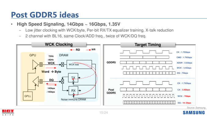
SK Hynix
As the memory manufacturer the most responsible for the development of HBM in the first place, SK Hynix’s Hot Chips presentation was all about HBM, its uses, and how technology developed from it can be used in other applications. There’s admittedly very little forward-looking about their presentation – the bulk of it was about why HBM is such a good fit for various applications and how they ensure reliability of the complex technology – but there was a brief discussion of where they want to go for HBM3.
The goal for HBM3 is to broaden its reach from high-end applications of today to a wider range of applications for tomorrow. No specific technologies or changes are proposed in SK Hynix’s slides, but at a high level it’s not too different from Samsung’s low-cost HBM proposal. Specifically, SK Hynix wants to make ECC an optional feature, and they want to make further changes to work on the cost and density of the technology. And of course, they also want to further improve on bandwidth, making HBM even faster at the high-end for the current types of devices that are already using HBM.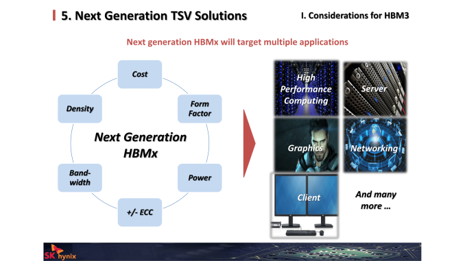
Xilinx
The last memory presentation I’ll be coving is from Xilinx. The firm is better known for their FPGAs and other forms of programmable logic, but they are also a major consumer of memory technologies and have their own ideas and concerns for how the memory ecosystem should advance.
 One interesting point made by Xilinx in their presentation was that, as you’d expect for stacking components, heat is an issue. The farther down the stack you go, the warmer it gets. Besides the absolute heat concerns – exceeding a safe temperate for the HBM stack – the fact that the different layers of the memory are running at different temperatures is also less than ideal (think temperature compensation and material expansion).
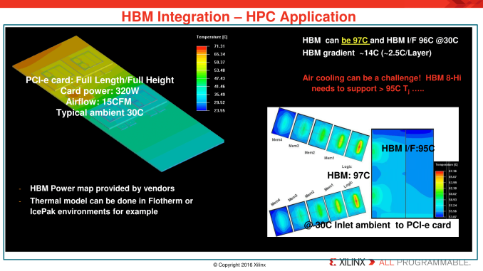
Xilinx is especially concerned here for what this means for 8-Hi stacks, which double the capacity of an HBM stack by doubling the number of DRAM layers. In practice this would make the lower DRAM and logic layers even more insulated, making them even hotter. And the sheer density of HBM (even an 8-Hi stack isn’t all that tall) makes those lower layers difficult to cool with air. As a result Xilinx is pushing for HBM to be developed so that it can withstand high Tjunction (Tj) temperatures, in order to ensure that air cooling of 8-Hi stacks is viable. To that end, Xilinx would like HBM’s TjMax to be over 95C, which is not an uncommon max temperature (GPUs and CPUs often have similar rules), but none the less illustrates how hot HBM can get.
Meanwhile their presentation also contains a handy chart of design rule comparisons for multi-die packaging. This is specifically useful for HBM, as the principles here will be useful for bringing HBM costs down. The silicon interposer is currently the only working option, but like the other presenters, Xilinx would like to have cheaper options in order to broaden the adoption of HBM. If all goes well, technologies like organic substrates and Wafer Level Fan Out may be two such solutions to the problem.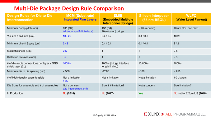
More...
-
08-23-16, 07:09 AM #6229
Anandtech: MSI Unveils the X99A Workstation Motherboard
Last week MSI introduced its new X99A Workstation motherboard, part of the X99 refresh we've seen over the past couple of months following the launch of the Broadwell-E processor line. Despite the name 'workstation', this board is based on the consumer-grade Intel X99 PCH rather than the server oriented parts, and as a result it supports overclocking. Part of the 'Workstation' feature set means that it has qualified support for NVIDIA Quadro PCIe cards, compatibility with ECC memory, and a U.2 connector for storage. The manufacturer claims that the mainboard uses special components that can improve the endurance of the board, although the warranty is still listed as three years.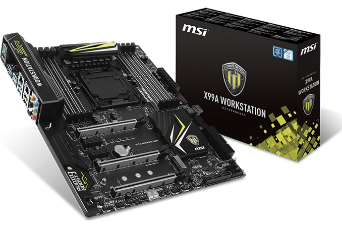
Typically, workstation-class motherboards for Intel Xeon E5 v3/v4 processors in LGA2011-3 packaging are based on the Intel C612 PCH, which has the same I/O features as the desktop-class Intel X99, but also supports a number of additional capabilities, which are important for business environments, such as vPro, RSTe, SVT and so on (you can read more about Intel’s 612 chipset here). When it comes to professional workstation vendors that supply machines to large corporations, those technologies make a lot of sense and are generally welcome. However, for prosumers and for many professionals working in small/medium businesses, these options might not be required, which is why a lot of motherboard manufacturers offer Intel X99-based workstation-class mainboards that fully support overclocking but continue to have numerous workstation features (such as support for ECC, when Xeon CPUs are installed). This is the focus of the X99A Workstation.
The MSI X99A Workstation (7A54) motherboard features one LGA2011-3 slot for Intel Core i7 as well as Intel Xeon E5 processors, though it is interesting to note that the maker does not list Intel Xeon SKUs in its qualified vendor list. Along with the eight-phase power delivery (which uses solid-state chokes), the mainboard carries eight DDR4 memory slots that not only support non-ECC/unbuffered memory modules with XMP 2.0 (and up to DDR4-3333 supported in OC modes), but also RDIMMs with ECC with applicable CPUs.
For add-in cards, the motherboard has three PCIe 3.0 x16 slots (which can work in x16, x16/x16, x8/x16/x8 modes with CPUs featuring 40 PCIe lanes) as well as two PCIe 2.0 x1 slots from the chipset.
When it comes to storage-related capabilities, the MSI X99A Workstation comes with one M.2-22110 slot, one U.2 port running in PCIe 3.0 x4 mode, and a SATAe port (unavailable when M.2 and U.2 are used). For traditional HDDs/SSDs/ODDs, the motherboard offers 10 SATA 6 Gb/s ports (including two ports from SATAe). So, in total the motherboard can support up to 12 storage devices.
The chipset diagram shows what is in play, and the M.2 configuration is a little odd given that 2 lanes come from the PCH and another two from the CPU despite standard CPU bifurcation stops at x4. In this instance I would have suggested that MSI merely considers the M.2 a CPU device with x4, given that the system would support it, but because Intel has 28-lane CPUs for the platform this can cause differences in bandwidth available. MSI shared the storage support matrix to help users looking into the X99A Workstation: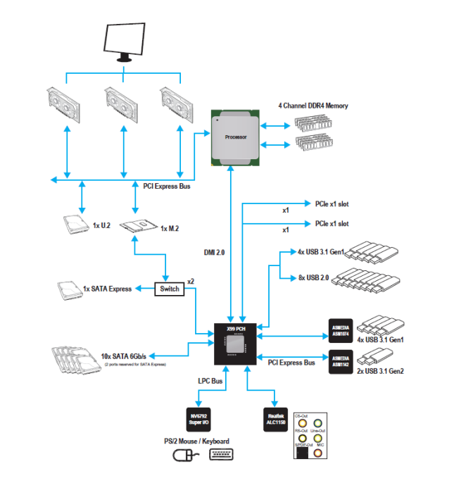
For audio and networking, the MSI X99A Workstation uses the Realtek ALC1150 solution (with PCB separation and filter caps) with 7.1-channel analog as well as S/PDIF outputs. For networking, the motherboard has an Intel I218LM and an Intel I210AT Gigabit LAN controllers, with teaming support listed. The mainboard also features ASMedia’s ASM1142 controller to enable one USB 3.1 Type-C (10 Gbps) and one USB 3.1 Type-A (10 Gbps) connectors on the rear panel. In addition, the motherboard supports eight USB 3.1 Type-A (5 Gbps) and eight USB 2.0 ports.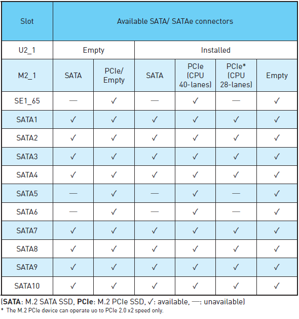
The MSI X99A Workstation should be available shortly, but pricing has not yet been decided.
Gallery: MSI Unveils X99A Workstation: Overclocking-Capable Motherboard for Workstations


More...
-
08-23-16, 08:25 AM #6230
Anandtech: G.Skill Shows Off Trident Z 8x8 GB and 8x16 DDR4-3333 Memory Kits
When Intel launched its new Core i7 Broadwell-E processors for high-end desktops earlier this year, all leading makers of motherboards released their new breed of Intel X99-based products that were supposedly 'optimized' for the new CPUs. Makers of memory modules are also beginning to roll-out their new DDR4 quad-channel kits that can operate at high frequencies with tight timings qualified for the new processors. At IDF this week, G.Skill demonstrated two new 64 GB and 128 GB kits designed for high-end workstations that require significant memory bandwidth.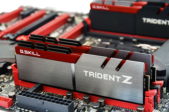
G.Skill’s upcoming quad-channel Trident Z 64 GB (8×8 GB) memory kit is rated to run at 3333 MT/s with CL13 13-13-33 latency settings at 1.35 V. Right now, the company only offers quad-channel 64 GB DDR4-3333 kits with CL16 18-18-38 timings (albeit, these are either 4×16 GB or 8×8 GB kits). Another upcoming Trident Z quad-channel kit has 128 GB (8×16 GB) capacity and can operate at 3333 MT/s with CL14 14-14-34 timings, which is considerably better when compared to CL16 18-18-38 latencies of currently available 128 GB DDR4-3333 kits from the company.
G.Skill claims that the Trident Z kits it demonstrated at IDF are based on Samsung’s 8 Gb DDR4 chips, but does not reveal whether these are ICs made using 20 nm or sub-20 nm process technology. More advanced DDR4 ICs coupled with the new memory controller inside Intel’s Broadwell-E CPUs could allow G.Skill to build new 64 GB and 128 GB DDR4-3333 HEDT kits with tight timings. It is to be expected that the company has managed to cherry-pick the right previous-gen ICs for its new memory modules and depending on the binning of such ICs, prices will be high.
The demonstrations at IDF were conducted using two systems equipped with Intel Core i7-6800K processors and ASUS ROG Rampage V Edition 10 or ASUS X99-Deluxe II motherboards. The PCs were running basic applications and did not require extensive cooling.
Traditionally, all Trident Z kits come equipped with aluminum heatsinks and feature Intel XMP 2.0 SPD profiles to make it easier for end-users to run them at their data-rates with the right timings and voltage. Expect the same features from the kits that G.Skill demonstrated at IDF.
The manufacturer did not announce when it plans to release its new Trident Z 64 GB DDR4-3333 CL13 and Trident Z 128 GB DDR4-3333 CL14 kits as well as their prices. Right now, G.Skill’s fastest 128 GB DDR4-3200 CL16 is available for $730 – $1042, depending on the retailer. Memory prices tend to be exponential at the high end, so these will cost a lot more.
Gallery: G.Skill Shows Off Trident Z 64 GB DDR4-3333 CL13 and 128 GB DDR4-3333 CL14 Memory Kits


More...


 Quote
QuoteThread Information
Users Browsing this Thread
There are currently 48 users browsing this thread. (0 members and 48 guests)


Bookmarks