

Results 6,711 to 6,720 of 12096
Thread: Anandtech News
-
02-08-17, 07:13 AM #6711
Anandtech: Logitech Launches the BRIO 4K Pro: Its First 4K UHD Webcam with HDR
Logitech has announced its BRIO 4K Pro Webcam, one of the world’s first webcams that features an Ultra HD resolution as well as HDR. The camera also has an infrared sensor to support facial recognition and Windows Hello.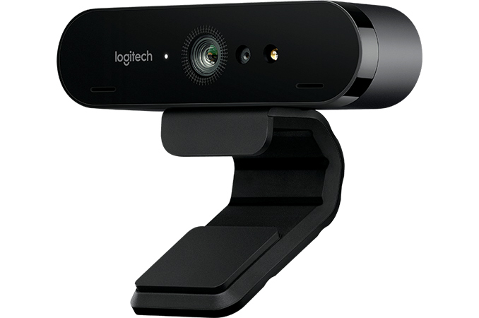
The Logitech BRIO aka 4K Pro Webcam (960-001105) is based on the company’s new 4K sensor, supports up to 4096×2160 resolution at 30 fps (or 1920x1080 at 60 fps), as well as RightLight 3 with HDR backlighting technology. The webcam has autofocus, 5X digital zoom, and is equipped with an infrared sensor. The BRIO can also select between 65°, 78°, and 90° field of view (FOV) options, and the device has two omni-directional microphones with additional noise cancellation options.
Logitech does not reveal a lot of information about its webcam and we do not know what codec it uses or what video encoder chip is inside. What we do know is that the webcam requires USB 3.0 interconnection for 4K video recording, which suggests that video bitrates it supports are fairly high. As with the recently released C922, the Brio 4K will use Logitech's latest software package which includes background replacement (similar to green screen detection). Logitech also lists a physical external privacy shutter on the feature set, allowing users to visually confirm that the camera is not taking video by other means (although, it is not mentioned if this also physically stops audio recording).
As for compatibility, the Logitech BRIO 4K Pro can work with all modern versions of Windows, Apple’s macOS 10.10 and higher as well as with Google Chrome OS version 29.0.1547.70. In addition, Logitech likes to point out that the webcam is suitable with multiple enterprise-class applications, including Skype for Business and Cisco programs with compatible certifications. It is worth noting that due to various reasons, Windows 7 supports up to 1080p only.
The Logitech BRIO 4K Pro webcam is designed to be attached to the top of a monitor, so weighs 63 grams (2.2 oz) while being 102 mm (4”) wide and 27 mm (1”) tall and 27 mm (1”) deep. The clip weighs 44 grams, making the whole construction around 107 grams total. Logitech lists that the webcam comes with a USB 3.0 Type-A cable, indicating a C-to-A connection rather than a straight C-to-C.
The Logitech BRIO 4K Pro Webcam is available today directly from Logitech.com as well as from the company’s resellers worldwide. The MSRP of the product is $199 in the U.S., £199 in the UK, and €239 in Europe (those last two include tax).
Gallery: Logitech Launches BRIO 4K Pro: Its First 4K UHD Webcam with HDR


More...
-
02-08-17, 09:49 AM #6712
Anandtech: Semi-Critical Intel Atom C2000 SoC Flaw Discovered, Hardware Fix Required
Last week, Paul Alcorn over at Tom’s Hardware picked up on an interesting statement made by Intel in their Q4 2016 earnings call. The company, whose Data Center group’s profits had slipped a bit year-over-year, was “observing a product quality issue in the fourth quarter with slightly higher expected failure rates under certain use and time constraints.” As a result the company had setup a reserve fund as part of their larger effort to deal with the issue, which would include a “minor” design (i.e. silicon) fix to permanently resolve the problem.
A bit more digging by Paul further turned up that the problem was with Intel’s Atom C2000 family, better known by the codenames Avoton and Rangeley. As a refresher, the Silvermont-based server SoCs were launched in Q3 of 2013 – about three and a half years ago – and are offered with 2, 4, and 8 cores. These chips are, in turn, meant for use in lower-power and reasonably highly threaded applications such as microservers, communication/networking gear, and storage. As a result the C2000 is an important part of Intel’s product lineup – especially as it directly competes with various ARM-based processors in many of its markets – but it’s a name that’s better known to device manufacturers and IT engineers than it is to consumers. Consequently, an issue with the C2000 family doesn’t immediately raise any eyebrows.
Jumping a week into the present, since their earnings call Intel has posted an updated spec sheet for the Atom C2000 family. More importantly, device manufacturers have started posting new product errata notices; and while they are keeping their distance away from naming the C2000 directly, all signs point to the affected products being C2000 based. As a result we finally have some insight into what the issue is with C2000. And while the news isn’t anywhere close to dire, it’s certainly not good news for Intel. As it turns out, there’s a degradation issue with at least some (if not all) parts in the Atom C2000 family, which over time can cause chips to fail only a few years into their lifetimes.
The Problem: Early Circuit Degradation
To understand what’s going on and why C2000 SoCs can fail early, let’s start with Intel’s updated spec sheet, which contains the new errata for the problem.
AVR54. System May Experience Inability to Boot or May Cease OperationAt a high-level, the problem is that the operating clock for the Low Pin Count bus can stop working. Essentially a type of legacy bus, the LPC bus is a simple bus for simple peripherals, best known for supporting legacy devices such as serial and parallel ports. It is not a bus that’s strictly necessary for the operation of a computer or embedded device, and instead its importance depends on what devices are being hung off of it. Along with legacy I/O devices, the second most common device type to hang off of the LPC is the boot ROM/BIOS– owing to the fact that it’s a simple device that needs little bandwidth – and this is where the C2000 flaw truly rears its head.
Problem: The SoC LPC_CLKOUT0 and/or LPC_CLKOUT1 signals (Low Pin Count bus clock outputs) may stop functioning.
Implication: If the LPC clock(s) stop functioning the system will no longer be able to boot.
Workaround: A platform level change has been identified and may be implemented as a workaround for this erratum.
As Intel’s errata succinctly explains, if the LPC bus breaks, then any system using it to host the boot ROM will no longer be able boot, as the system would no longer be able to access said boot ROM. The good news is that Intel has a workaround (more on that in a second), so it’s an avoidable failure, but it’s a hardware workaround, meaning the affected boards have to be reworked to fix them. Complicating matters, since Atom C2000 is a BGA chip being used in an embedded fashion, an LPC failure means that the entire board (if not the entire device) has to be replaced.
Diving deeper, the big question of course is how the LPC bus could break in this fashion. To that end, The Register reached out to Intel and has been able to get a few more details. As quoted by The Register, Intel is saying that the problem is "a degradation of a circuit element under high use conditions at a rate higher than Intel’s quality goals after multiple years of service."
Though we tend to think of solid-state electronics as just that – solid and unchanging – circuit degradation is a normal part of the lifecycle of a complex semiconductor like a processor. Quantum tunneling and other effects on a microscopic scale will wear down processors while they’re in use, leading to eventual performance degradation or operational failure. However even with modern processors the effect should take a decade or longer, much longer than the expected service lifetime of a chip. So when something happens to speed up the degradation process, if severe enough it can cut the lifetime of a chip to a fraction of what it was planned for, causing a chip (or line of chips) to fail while still in active use. And this is exactly what’s happening with the Atom C2000.
For Intel, this is the second time this decade that they’ve encountered a degradation issue like this. Back in 2011 the company had to undertake a much larger and more embarrassing repair & replacement program for motherboards using early Intel 6-series chipsets. On those boards an overbiased (overdriven) transistor controlling some of the SATA ports could fail early, disabling those SATA ports. And while Intel hasn’t clarified whether something similar to this is happening on the Atom C2000, I wouldn’t be too surprised if it was. Which isn’t to unnecessarily pick on Intel here; given the geometries at play (bear in mind just how small a 22nm transistor is) transistor reliability is a significant challenge for all players. Just a bit too much voltage on a single transistor out of billions can be enough to ultimately break a chip.
The Solution: New Silicon & Reworked Motherboards
Anyhow, the good news is that Intel has developed both a silicon workaround and a platform workaround. The long-term solution is of course rolling out a new revision of the C2000 silicon that incorporates a fix for the issue, and Intel has told The Register they’ll be doing just that. This will actually come somewhat late in the lifetime of the processor, as the current B0 revision was launched three and a half years ago and will be succeeded by Denverton this year. At the same time though, as an IT-focused product Intel will still need to offer the Atom C2000 series to customers for a number of years to come, so even with the cost of a new revision of the silicon, it’s in Intel’s long-term interest.
More immediately, the platform fix can be used to prevent the issue on boards with the B0 silicon. Unfortunately Intel isn’t disclosing just what the platform fix is, but if it is a transistor bias issue, then the fix is likely to involve reducing the voltage to the transistor, essentially bringing its degradation back to expected levels. Some individual product vendors are also reporting that the fix can be reworked into existing (post-production) boards, though it sounds like this can only prevent the issue, not fix an already-unbootable board.
Affected Products: Routers, Servers, & NASes
As a result of the nature of a problem, the situation is a mixed bag for device manufacturers and owners. First and foremost, while most manufacturers have used the LPC bus to host the boot ROM, not all of them have. For the smaller number of manufacturers who are using SPI Flash, this wouldn't impact them unless they were using the LPC bus for something else. Otherwise for those manufacturers who are impacted, transistor degradation is heavily dependent on ambient temperature and use: the hotter a chip and the harder its run, the faster a transistor will degrade. Consequently, while all C2000 chips have the flaw, not all C2000 chips will have their LPC clock fail before a device reaches the end of its useful lifetime. And certainly not all C2000 chips will fail at the same time.
Cisco, whose routers are impacted, estimates that while issues can occur as early as 18 months in, they don’t expect a meaningful spike in failures until 3 years (36 months) in. This of course happens to be just a bit shorter than the age of the first C2000 products, which is likely why this issue hasn’t come to light until now. Failures would then become increasingly likely as time goes on, and accordingly Cisco will be replacing the oldest affected routers first, as they’re the most vulnerable to the degradation issue.
As for other vendors shipping Atom C2000-based products, those vendors are setting up their own support programs. Patrick Kennedy over at ServeTheHome has already started compiling a list of vendor responses, including Supermicro and Netgate. However as it stands a lot of vendors are still developing their response to the issue, so this will be an ongoing process.
Finally, what’s likely to be the most affected on the consumer side of matters will be on the Network Attached Storage front. As pointed out to me by our own Ganesh TS, Seagate, Synology, ASRock, Advantronix, and other NAS vendors have all shipped devices using the flawed chips, and as a result all of these products are vulnerable to early failures. These vendors are still working on their respective support programs, but for covered devices the result is going to be the same: the affected NASes will need to be swapped for models with fixed boards/silicon. So NAS owners will want to pay close attention here, as while these devices aren’t necessarily at risk of immediate failure, they are at risk of failure in the long term.
Sources: Tom's Hardware, The Register, & ServeTheHome
More...
-
02-08-17, 01:17 PM #6713
Anandtech: Mediatek Announces the P25: A Faster P20 with Support for Dual Camera
With all the smartphone-based talk about the leading edge of the industry focusing on upcoming 10nm chips, it might be easy to forget that the majority of smartphones sold in 2017 will still be on 16nm or 28nm and are more likely to be A72/A53 based rather than A73 or custom cores. Earlier this year we have already seen the launch of the Xiaomi Redmi Note 4 in India, with a surprising twist: Xiaomi downgraded the SoC in that phone (with lower peak performance) over the Note 3 due to the power saving advantages of using eight ARM Cortex A53 cores on 16nm in the Snapdragon 625 over using a 2+4 configuration of A72/A53 as seen in the Note 3 on 28m. At the time we postulated that this is going to be a trend through 2017: we’ll see mid-range smartphones go after power efficiency with smaller cores and smaller chips on more power efficient processes in exchange for performance. Nonetheless, the power efficient chip does still need some performance, and Mediatek is announcing the P25 for this. The P25 features a significant step up from the P10, and speed boost to the P20. This allows the P25 to support dual cameras as well.
The P20 was perhaps not as popular as Mediatek would have liked in 2016: it was in the Elephone P20 and the UMI Plus E, but that’s about it. By contrast, the P10 was popular. To entice handset developers to drop in a better chip to the updates for these devices in 2017, the P25 adds another 200 MHz into the cores over the P20, as well as increasing the internal Turbo Engine for a 30-35% performance boost. This allows the DSP to support dual cameras, up to 13MP+13MP, and puts it directly in line against devices such as the dual-camera based Honor 6X which uses the Kirin 655. The P25 also retains the support for dual channel LPDDR4X up to 6GB.MediaTek 2017 H1 20-Series Lineup SoC X20 X23 X25 X27 P20 P25 CPU 2xA72 2.10 GHz 2.30 GHz 2.50 GHz 2.70 GHz - - 4xA53 1.85 GHz 1.85 GHz 2.00 GHz 2.00 GHz 2.3 GHz 2.5 GHz 4xA53 1.40 GHz 1.40 GHz 1.55 GHz 1.60 GHz 2.3 GHz 2.5 GHz Memory
(32-bit)LPDDR3 1 x 800MHz 1 x 933 MHz LPDDR4X 2 x 1600 MHz GPU T880MP4
@780 MHzT880MP4 @850 MHz T880MP4 @875 MHz T880MP2
@900MHzEncode 2160p30 HEVC w/HDR 2160p30 H.264 Decode 2160p30 10-bit H.264/HEVC/VP9 2160p30 H.264 & HEVC Camera
/ISPSingle Dual 32MP ISP @ 24fps 24MP 24MP Dual ? - 2x13MP Modem LTE Cat. 6 300/50 with 2x20 CA Mfc. Process 20SoC 16nm FinFET
The rest of the P25 is similar to the older SoC: 4K30 decode for HEVC, 4K30 encode for H.254, integrated ARM Mali T880MP2 graphics, and a Cat 6 modem with support for 2x20 MHz carrier aggregation. Both SoCs support a screen resolution of Full HD at 60 FPS.
Given today’s announcement, it is highly likely that the P25 has been shipping to customers for long enough to perhaps see some design wins for Mobile World Congress, which starts at the end of February. There will be three of us at the show, so stay tuned for our coverage.
More...
-
02-09-17, 03:56 PM #6714
Anandtech: Intel to Equip Fab 42 for 7 nm
Intel this week announced plans to bring its Fab 42 online to produce semiconductors using a 7 nm fabrication process. It will take three to four years, and the move will cost Intel several billions of dollars but will create approximately 3,000 of high-tech jobs in Chandler, Arizona. Unfortunately, Intel did not share details about its 7 nm manufacturing technology at this time.
Intel began construction of its Fab 42 back in 2011 with the aim to build the most advanced, high-volume chip production facility in the world. The building was completed in 2013, but instead of moving in equipment to produce chips using 14 nm fabrication process, Intel decided to postpone its completion in early 2014. The site is equipped with heating, air conditioning, and other essential things, but no actual semiconductor manufacturing equipment has been installed. Intel still has no immediate public plans to use the Fab 42 for the production of chips using its 10 nm process technology in the short-term future but has indicated it intends to use it for its 7 nm ICs several years down the road.
Intel intends to spend as much as $7 billion to equip Fab 42, but at the moment the company does not share what kind of tools it plans to install. As a result we have no new information about Intel's 7 nm technology. Intel has implied that it could start using extreme ultraviolet (EUV) lithography at 7 nm, but has never committed to the plan. Earlier this year the company said it would invest in a 7 nm pilot line in one of its development sites, but did not elaborate beyond that. One of the things that the CEO of Intel disclosed about the 7 nm in general in his email to employees this week is that it requires “an increasing amount of factory space per wafer.” This possibly means that Intel will insert EUV equipment into the process technology for cirical layers and will continue to use a lot of multipatterning, which increases the diversity requirements for the production tools.
Intel believes that when completed, Fab 42 will be the most advanced semiconductor wafer fab in the world that will create 3,000 direct high-tech jobs and 10,000 direct and indirect jobs in total. It should be noted that the semiconductor company will not start to move in equipment into the Fab 42 before it figures out all the peculiarities of the 7 nm manufacturing technology. Once it finalizes the pilot line and is satisfied with the equipment performance, it starts to replicate the line at different sites.
Intel said that it will use its 7 nm fabrication process to produce various processors for PCs, data centers and other devices that will be used for AI, automated driving, medical research/treatment as well as other applications. So, as usually, the manufacturing technology will be positioned to make the whole stack of Intel’s products several years from now.
Related Reading:
- Intel Announces Record Quarterly Revenue And Full-Year Revenue For Q4'2016
- Intel Compute Card: A Universal Compute Form-Factor for Different Kinds of Devices
- CES 2017: Intel Press Event Live Blog
More...
-
02-09-17, 05:40 PM #6715
Anandtech: NEC Goes for a Curved Display, Launches 3440×1440 MultiSync EX341R Monitor
This week NEC has announced its first curved ultrawide display, the EX341R. NEC is promoting the panel for offices, control rooms, trading rooms, and other applications that typically use multi-monitor configurations but also appreciate color accuracy. The screen has a number of differences when compared to displays for gamers, and the price of the new MultiSync EX341R will be reflected in this.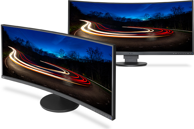
In the recent years, NEC concentrated on displays for commercial and professional use, whereas its consumer monitor lineup slowly stepped into the background. The majority of curved ultrawide displays nowadays are designed with gamers in mind, which is why manufacturers tend to incorporate very high refresh rates along with dynamic refresh rate technologies and gaming specific features or aesthetics. Nonetheless, ultrawide displays may make sense to replace those used to multi-monitor environments, and this is a reason why Dell introduced its business-oriented curved ultrawide screens last year. NEC now also sees demand for monitors with a 21:9 aspect ratio from its customers, which is why the company announced its new MultiSync EX341R-BK and EX341R-SV-BK products this week.
The NEC MultiSync EX341R-series displays are based on SVA panels (presumably made by Samsung) with a 3440×1440 resolution, a 1000:1 contrast ratio, 290 nits brightness, 178°/178° viewing angles, 5 ms response time and a 60 Hz refresh rate. It also targets customers that need various degrees of color accuracy (NEC markets the panels as supporting 99.5% sRGB) and therefore bundles the Spyder5 color calibration sensor and the SpectraView II software with the EX341R-SV-BK monitor.
As for connectivity, the NEC MultiSync EX341R has one DisplayPort 1.2 with MST support as well as two HDMI headers (one 1.4 and one 2.0). The monitor fully supports NEC’s control Sync technology that allows controlling the settings of up to 25 displays in a multi-monitor setup using controls of only one of them. Additionally, the display supports PBP and PiP features when connected to two computers. Finally, it has a quad-port USB 3.0 hub with two USB Type-B upstream ports (to connect to two different PCs).
The NEC MultiSync EX341R-BK and EX341R-SV-BK displays will be available in February at an MSRP of $999 and $1,149 respectively.NEC's MultiSync EX341R-Series Displays EX341R-BK EX341R-SV-BK Panel 34" SVA Native Resolution 3440 × 1440 Maximum Refresh Rate 60 Hz Response Time 5 ms Brightness 290 cd/m² Contrast 3000:1 Viewing Angles 178°/178° horizontal/vertical Curvature 1800R Pixel Pitch 0.23 mm Pixel Density 110 ppi Color Gamut NTSC: 77.5%
sRGB: 99.5%
'16.7 million colors'Inputs 1 × DisplayPort 1.2
1 × HDMI 2.0
1 × HDMI 1.4Outputs DisplayPort 1.2 (SST/MST) USB Hub 4-port USB 3.0 hub
2 × USB Type-B upstream portsAudio 1 W × 2
audio in/out portsPower Consumption (idle/active) Idle: 0.26 W
Active: 62 WProduct Bundle Setup sheet
User manual
Power cord
DisplayPort cable
USB cable
ControlSync cableSetup sheet
User manual
Power cord
DisplayPort cable
USB cable
ControlSync cable
SpectraViewII Software USB
Spyder5 Color Calibration SensorLaunch Price $999 $1150
Gallery: NEC Multisync EX341R-BK and EX341R-SV-BK Displays


Related Reading:
- Dell Unveils UltraSharp U3417W: Makes Its Curved Display More Curved
- Acer Launches Curved XR382CQK Display: 37.5-inch, 3840×1600, FreeSync, & USB-C
- AOC Announces the AGON AG352UCG 21:9 Curved Display: 35", 3440×1440, 100Hz with G-Sync
- Philips BDM4037UW Goes on Sale: 40 Inch 4K Curved Display for $800
More...
-
02-09-17, 06:20 PM #6716
Anandtech: Intel Confirms 8th Gen Core on 14nm, Data Center First to New Nodes
A quick news piece on information coming out of Intel’s annual Investor Day in California. As confirmed to Ashraf Eassa by Intel at the event, Intel’s 8th Generation Core microarchitecture will remain on the 14nm node. This is an interesting development with the recent launch of Intel’s 7th Generation Core products being touted as the ‘optimization’ behind the new ‘Process-Architecture-Optimization’ three-stage cadence that had replaced the old ‘tick-tock’ cadence. With Intel stringing out 14nm (or at least, an improved variant of 14nm as we’ve seen on 7th Gen) for another generation, it makes us wonder where exactly Intel can promise future performance or efficiency gains on the design unless they start implementing microarchitecture changes.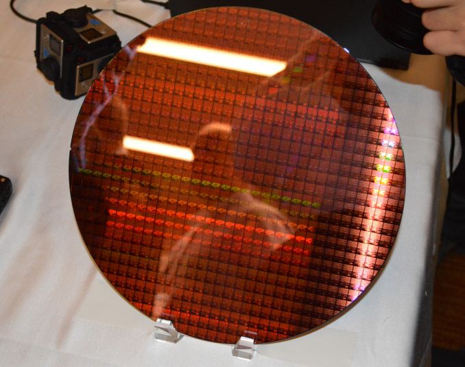
Despite this, if you were to believe supposed ‘leaked’ roadmaps (which we haven’t confirmed from a second source as of yet), the 8th Generation product ‘Cannon Lake’ is more geared towards the Y and U part of Intel’s roadmap. This would ring true with a mobile first strategy that Intel has mirrored with recent generations such that the smaller, low power chips are off the production line for a new product first, however we'd also expect 10nm to also be in the smaller chips first too (as demonstrated at CES). Where Cannon Lake will end up in the desktop or enterprise segment however remains to be seen. To put something a bit more solid into this, Ashraf also mentioned words from Dr. Venkata ‘Murthy’ Renduchintala, VP and GM of Client and IoT:
‘Murthy referred to it at the event, process tech use will be ‘fluid’ based on segment’.If one read too much into this, we may start seeing a blend of process nodes for different segments at the same time for different areas of the market. We already do have that to some extent with the mainstream CPUs and the HEDT/Xeon families, but this phrasing seems that we might get another split between consumer products or consumer and enterprise. We may get to a point where Intel's 'Gen' naming scheme for its CPUs covers two or more process node variants.
Speaking of the Enterprise segment, another bit of information has also surfaced, coming from a slide during a talk by Diane Bryant (EVP/GM of Data Center) and posted online by Ashraf. The slide contains the words ‘Data center first for next process node’
We can either talk about process node in terms of the ‘number’, either 14nm/10nm/7nm, or by variants within that process (high power, high efficiency). One might suspect that this means Intel is moving hard and fast with 10nm for Xeons and big computing projects, despite showing off 10nm silicon at CES earlier this year. That being said, it’s important to remember that the data center market is large, and includes high-density systems with many cores, such as Atom cores, and Intel did recently open up its 10nm foundry business to ARM Artisan IP projects. So while the slide does say ‘Data center first’, it might be referring to DC projects based on ARM IP in that segment rather than big 4-24+ core Xeons. At this stage of the game it is hard to tell.
On top of all this, Intel still has extreme confidence in its foundry business. An image posted by Dick James of Siliconics from the livestream shows Intel expects to have a three-year process node advantage when its competitors (Samsung, TSMC) start launching 10nm:
I’ve been brief with this news for a reason - at this point there are a lot of balls in the air with many different ways to take this information, and the Investor Day is winding down on talks and finishing with smaller 1-on-1 meetings. We may get further clarification on this news as the day goes on.
Gallery: Intel Confirms 8th Gen Core on 14nm, Data Center First to New Nodes


More...
-
02-09-17, 09:40 PM #6717
Anandtech: NVIDIA Reports Q4 2017 And Fiscal 2017 Results: Record Revenue
NVIDIA’s fiscal year for 2017 ended on January 29, 2017, and for the fourth quarter and full year, NVIDIA reports they had record revenues. For Q4 2017, NVIDIA is reporting revenue of $2.173 billio.n, up 55% from a year ago. Gross margin came in at 60.0%, which is up 3.5% from Q4 2016. Operating income for the quarter was $733 million, up 191%, and net income was up 216% to $655 million. The very high growth in operating income and net income are even more impressive, since Q4 2016 was also a record for them at the time. NVIDIA reported $0.99 per share earnings for this quarter, up 183%.
Even though 2016 was a record year for NVIDIA, 2017 was even better. NVIDIA reported record revenue of $6.91 billion for the full fiscal year 2017, which is up 38% from a year ago, and had a net income of $1.666 billion. Earnings per share for the year were $2.57. They also repurchased $739 million in shares over the last year, and paid $261 million in dividends.NVIDIA Q4 2017 Financial Results (GAAP) Q4'2017 Q3'2017 Q4'2016 Q/Q Y/Y Revenue (in millions USD) $2173 $2004 $1401 +8% +55% Gross Margin 60.0% 59.0% 56.5% +1.0% +3.5% Operating Income (in millions USD) $733 $639 $252 +15% +191% Net Income $655 $542 $207 +21% +183% EPS $0.99 $0.83 $0.35 +19% +183%
The majority of NVIDIA’s revenue came from their Gaming segment, which includes their GeForce GPUs. The launch of Pascal has clearly been very successful, and for the quarter NVIDIA’s Gaming segment had revenues of $1.348 billion, up from $810 million a year ago. This is a gain of 66.4% year-over-year, on a market they were already at the top of. This quarter, they also launched the GeForce GTX 1050 and 1050 Ti mobile GPUs, and a new SHIELD TV, along with unveiling the GeForce NOW game streaming service.
Professional Visualization had much more modest growth, being up “only” 10.8% from last year, with revenues of $225 million for the quarter. They just launched the GP100 Quadro though, so it may have even more growth to come.
Datacenter has been a big focus from NVIDIA in diversifying their portfolio, and this quarter they had some announcements here as well, with a collaboration with Microsoft on the Microsoft Cognitive Toolkit, powered by Microsoft Azure cloud running on NVIDIA DGX-1 deep learning system. They unveiled the DGX SATURNV AI supercomputer, and partnered with the National Cancer Institute and US Department of Energy to build CANDLE to “advance cancer research”. The growth of NVIDIA’s Datacenter segment has been almost exponential, and it is now the second largest source of revenue for the company. For Q4 2017, NVIDIA reported $296 million in revenue from this segment, up from $97 million a year ago, or an increase of 205.1%.
NVIDIA has also diversified into Automotive with their Tegra lineup, after originally releasing it as a mobile SoC. This has also been a boon for the company, and they are now powering self-driving cars, and the infotainment systems of major manufacturers like Audi, and Mercedes-Benz, and they’ve partnered with Bosch on self-driving systems as well. This segment saw revenues of $128 million for the quarter, up from $93 million a year ago, or 37.6%.
Finally, the OEM and IP segment had revenues of $176 million, down from $198 million a year ago. Although this dropped, it’s likely due to the loss of the $66 million/quarter they were receiving from Intel as part of the settlement agreement made in 2011, which Intel paid it’s last payment in January 2016.
For next quarter, NVIDIA is expecting revenues of $1.9 billion, plus or minus 2%, and gross margins between 59.5 and 59.7%.NVIDIA Quarterly Revenue Comparison (GAAP) In millions Q4'2017 Q3'2017 Q4'2016 Q/Q Y/Y Gaming $1348 $1244 $810 +8.4% +66.4% Professional Visualization $225 $207 $203 +8.7% +10.8% Datacenter $296 $240 $97 +23.3% +205.1% Automotive $128 $127 $93 +0.8% +37.6% OEM & IP $176 $186 $198 -5.4 -11.1%
The diversification of NVIDIA from a purely GPU company has clearly paid dividends, especially when their core market is doing as well as it is. The datacenter growth is clearly very high margin as well, considering the jump in net income for the quarter.
Source: NVIDIA Investor Relations
More...
-
02-10-17, 08:25 AM #6718
Anandtech: The Patriot Hellfire M.2 480GB Review: Phison NVMe Tested
The Patriot Hellfire M.2 PCIe SSD is Patriot's first NVMe SSD, and one of several similar products based on Phison's E7 NVMe controller paired with Toshiba 15nm MLC. The Patriot Hellfire is an entry-level PCIe SSD that is largely free of the pitfalls of Intel's cheaper but TLC-based SSD 600p.
More...
-
02-11-17, 08:21 AM #6719
Anandtech: GlobalFoundries to Expand Capacities, Build a Fab in China
GlobalFoundries has announced plans to expand manufacturing capacities for its leading edge and mainstream production technologies in the U.S., Germany and Singapore. After the upgrades of the fabs are completed, the total 300-mm output of the company will increase by approximately 20%. In addition, GlobalFoundries intends to build a new 300mm fab in Chengdu, China, in a partnership with local authorities. The latter will produce chips using 130/180 nm and FD-SOI manufacturing technologies.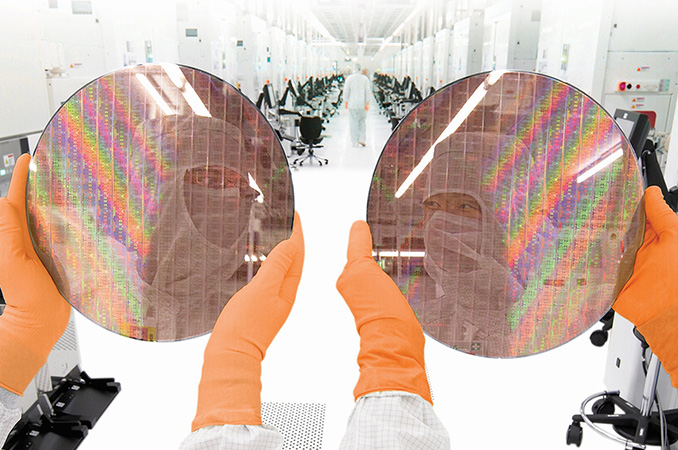
Fab 8 to Gain 20% 14LPP FinFET CapacityGlobalFoundries' Expansion Plans Process Technologies
current and plannedCurrent Capacity*
wafer starts per monthPlanned Increase Target Capacity*
wafer starts per monthTarget Timeframe Fab 1
(Dresden, Germany)32 nm SOI
28 nm
22FDX (FD-SOI)
12FDX (FD-SOI)80,000 +40% ~110,000 2020 Fab 7
(Singapore)130 nm
65/55 nm
40 nm
RF-SOI68,000 +35% for 40 nm Over 68,000 Coming years Fabs
(Singapore)180 nm unknown +?% for 180 nm unknown Coming years Fab 8
(New York, USA)28 nm
14LPP
7 nm60,000 +20% for 14LPP Over 60,000 Early 2018 Chengdu Fab
(China)180/130 nm
22FDX (FD-SOI)- - Ph. 1: 20,000
Ph. 2: 65,000
P1+P2: 85,000Ph. 1: 2018
Ph. 2: 2019*Please note that actual wafer starts per month (WSPM) output of a fab depends on multiple factors, including process technologies used. As a result, all the WSPM capacity numbers are relative and may not reflect actual performance. Keep in mind, that as foundries and IDMs increase usage of multi-patterning techniques, their effective WSPM output drops as wafers spend more time in the cleanroom. Hence, to keep the wafer starts per month capacity, chipmakers need to add equipment (which may, or may not, involve physical expansion of the cleanroom space).
GlobalFoundries operates 10 fabs worldwide with four of them processing 300 mm wafers. The company’s most advanced fab is the Fab 8 located in Luther Forest Technology Campus (Saratoga County, New York) where the chipmaker produces flagship processors for AMD and some other leading developers of chips. To keep the Fab 8 up-to-date, GlobalFoundries spends billions of dollars on development of new manufacturing technologies and production equipment. Back in September, the company already announced plans to invest several billion in new tools to produce ICs (integrated circuits) using its 7 nm fabrication process and this week GlobalFoundries said it would invest in the expansion of the Fab 8’s manufacturing capacity.
After the latest expansion in 2013, the Fab 8’s capacity is around 60,000 wafer starts per month. The exact capacity today depends on several factors because the company now processes wafers using a more advanced process technology (the 14LPP) that uses multi-patterning, which effectively reduces capacity because each wafer spends more time in the cleanroom. In a bid to increase the output of 14LPP FinFET ICs by 20% by early 2018, the company intends to boost its production capacity. The firm said that the expansion does not involve physical expansion of the cleanroom, but the installation of additional more advanced step-and-scan systems and/or other tools into the existing space. For example, a switch from the TWINSCAN NXT:1960Bi to the TWINSCAN NXT:1980Di increases output of wafers by around 20% as the latter can process 275 wafers per hour versus 230 wafers per hour. GlobalFoundries Fab 8. Photo by FinanceFeeds.net
As the company is preparing to start high-volume manufacturing (HMV) of chips using its 7 nm FinFET technology in the second quarter of next year (so, several months ahead of the plan), the actual output of the Fab 8 remains to be seen. Initially, GlobalFoundries plans to use deep ultraviolet (DUV) lithography with quadruple patterning to produce chips using its 7 nm process, but sometime in 2019 it intends to start using extreme ultraviolet (EUV) lithography for a new wave of 7 nm designs. Usage of EUV will not eliminate multi-/quadruple-patterning, but will be used for cirical layers and will thus help to increase output of leading-edge chips. At present, the company does not talk about its 7 nm capacity, but it is logical to assume that the current expansion will have a positive effect on it as well.
In fact, the expansion of the Fab 8 is important for the fabless semiconductor industry as a whole because there are not a lot of foundries capable of producing ICs using FinFET manufacturing technologies. While numerous companies (like TowerJazz and Vanguard) ceased to develop leading-edge fabrication processes quite some time ago, SMIC and UMC are struggling with FinFETs as well. Moreover, neither of them are adopting FD-SOI-based planar technologies. As a result, there are only three pure-play foundries to offer HMV FinFETs to fabless chip designers: GlobalFoundries, Samsung Foundry and TSMC (Intel's 10nm ARM Artisan IP foundry business is potentially to add to that list in due course). Besides, there are two companies to offer advanced FD-SOI-based planar technologies: GF and Samsung.
Fab 1 Gets More FD-SOI
Fab 1 used to be AMD’s flagship production facility and it remains GlobalFoundries’ highest-capacity plant that can process up to 80,000 wafers per month. While it does not produce chips using the most advanced technologies with FinFETs, it is used to make energy-efficient ICs using low-power and cost-optimized planar FD-SOI-based manufacturing processes. Since the development of FinFET-based chips costs significantly more than the development of ICs with planar transistors, planar process technologies continue to make sense for many designers of chips (especially smaller ones). To fulfill demand from such customers developing ICs for Internet of Things (IoT), smartphone, automotive electronic and other applications, GlobalFoundries plans to expand the capacity of the Fab 1 by 40% by 2020 (it is only going to expand the FD-SOI lines). GlobalFoundries did not elaborate whether the expansion involves the construction of new buildings, the physical increase of the cleanroom space of one (or both) of the two fab modules or installation of new equipment.
At present, the company offers a variety of planar manufacturing processes at Fab 1, including various 28 nm bulk technologies as well as its FD-SOI 22FDX (it uses back-end-of-line interconnect flow of STMicroelectronics’ 28nm FD-SOI, as well as front-end-of-line STM’s 14nm FD-SOI process technology). GlobalFoundries pins a lot of hopes on the FD-SOI technology and the significant expansion of the Fab 1 re-emphasizes this commitment.
The expansion of the factory will help to boost not only 22FDX output, but could also offer significant production capacities for developers designing for the next-gen FD-SOI technology, 12FDX (we do not say that all of the new equipment will be re-used for the 12FDX, but at least some tools will be). GlobalFoundries does not release too many details about the 12FDX process to the public, but it says that it enables “the performance of 10 nm FinFET with better power consumption and lower cost than 16nm FinFET,” while also offering a 15% geometry scaling benefit compared to “today’s FinFET technologies” (if by “today’s” GF means 14LPP and CLN16FF/FF+, then the 12FDX has a 15% higher transistor density compared to technologies based on 20 nm BEOLs). The company expects the first 12FDX tape-outs in the first half of 2019, so the expansion of the Fab 1 by 2020 will likely be a benefit for FD-SOI designers in general.
The First Fab in China
Meanwhile, GlobalFoundries’ FD-SOI efforts will not be limited to its Germany manufacturing facility (even though the Fab 1 will remain the key development site for the tech). The company’s first fab in China (which might be called the Fab 11, but we will call it the Chengdu fab for now) will also be able to produce chips using the 22FDX. But before jumping to the FD-SOI in China, let’s talk about the plant itself first.
The Chengdu fab will be built in a partnership between GlobalFoundries and the Chengdu municipality. The first phase of the fab will begin operations in 2018 and it will use mainstream 180/130 nm fabrication technologies. The fab will initially process around 20,000 wafers per month. It is important to note that the mainstream manufacturing technologies that the Chengdu fab will use were originally developed by Chartered and not by AMD for its CPUs. The second phase will start operations in 2019 and will eventually be able to process 65,000 wafers per month using the 22FDX technology.
When fully ramped, the Chengdu fab will have a capacity of approximately 1,000,000 wafers per year (so, around 83,000 ~ 85,000 wafers per month for the phase 1 and phase 2) and will be a tangible manufacturing asset for GlobalFoundries. The fab is meant to fulfill increasing demand from China-based developers of semiconductors, but it will also be used to make chips for other fabless companies using primarily the 22FDX process, further increasing FD-SOI manufacturing capacities of GlobalFoundries and making the tech more attractive to customers requiring very high product volumes.
It is noteworthy that one of the interested parties in GF’s 22FDX tech is Rockchip, which has so far used only bulk process technologies of TSMC, SMIC and GlobalFoundries to produce its mobile SoCs. Other adopters of FD-SOI are developers of various wireless chips (like modems) and ICs that have to be very energy-efficient (particularly in idle mode).
Singapore Fabs Get a Boost
Finally, in addition to expanding the leading edge Fab 1 and Fab 8 as well as building a new semiconductor manufacturing facility, GlobalFoundries intends to increase the output of its fabs in Singapore.
The company does not publish too many details about the Singapore expansion, but only says that it intends to increase 40 nm capacity at its 300-mm Fab 7 by 35% and also boost output of its lines processing wafers using its 180 nm manufacturing process. Furthermore, GlobalFoundries will install new tools to make chips using its RF-SOI fabrication tech presumably on 300 mm wafers (which may be a big deal).
The Right Capacity at the Right Time
Since modern fabs and production tools cost billions of dollars to build, semiconductor manufacturers typically cannot afford them standing idle. A lack of capacity means that foundries cannot land orders from customers and eventually lose market share to rivals. Therefore it is important to have the right capacity and process technologies at the right time.
According to IC Insights, sales of all pure-play foundries in 2016 totaled around $50 billion, growing 11% year-over-year. GlobalFoundries was the second largest contract maker of chips with an estimated $5.5 billion in revenue (keep in mind that the company does not officially comment on such numbers), up 10% YoY. In a bid to sustain growth, GlobalFoundries needs to gradually increase its production capacities and the installation of new tools will serve the purpose, just like building a new fab in China.
For foundries, expanding production capacities is a usual business and they always try to optimize their output to meet demands from customers. GlobalFoundries is selectively adding capacities to popular nodes (and companies like MediaTek, Qualcomm, and Rockchip have already welcomed the decision), which is a smart move. In addition, it plans to build a new fab in China, which is a clever way to address a particular territory.
Related Reading:
- GlobalFoundries Updates Roadmap: 7 nm in 2H 2018, EUV Sooner Than Later?
- Intel to Equip Fab 42 for 7 nm
- Samsung Foundry Announces 10nm SoC In Mass-Production
- EUV Lithography Makes Good Progress, Still Not Ready for Prime Time
More...
-
02-11-17, 10:53 AM #6720
Anandtech: Eurocom Launches a 780 W External PSU for Laptops
The world is getting mobile and many things that used to come in full-tower desktop chassis are now available in mobile form-factors. For example, high-performance notebooks from companies like Eurocom, Clevo or MSI can easily leave mid-range mainstream desktops behind in terms of performance - and yet these are laptops (albeit, not very portable ones). These machines typically come with a single large power adaptor, or in the case of a couple of models, two adaptors. To add to the market, Eurocom this week announced its new high efficiency 780 W power supply/AC/DC adapter.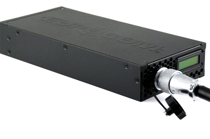
The new Eurocom 780 W external PSU is designed for PCs that use a four-conductor DIN-type connector, which includes ultra-high-end laptops like Eurocom’s own Sky X9E2, Sky X7E2 as well as some notebooks from Clevo (including PCs that this manufacturer produces for other brands and which use the same power plug) and MSI. The power supply can also be used for other PCs including compact desktops/workstations/servers or even industrial systems used in rough conditions.
The 780 W external PSU is rated for a 39 A maximum load (below that of high-end desktop PSUs), which is a very high load for laptops. Eurocom claims that efficiency of the 780 W external power supply is higher than 90% when measured with a nominal line and maximum load (the company does not mention environment temperature), but it is not 80 PLUS certified. To cool down the internal components, the device has two high-speed fans, which may mean noise. Finally, the PSU is equipped with a LED display that gives a real-time breakdown of the amperage, voltage and wattage currently used.
Eurocom’s laptops in certain configurations use two 330 W PSUs with a converter box, which is not very convenient. The new Eurocom 780 W AC/DC Adapter solves the problem to a degree, but keep in mind that the PSU alone will be big and heavy: it weighs 1.7 kilograms with the cable (3.75 lbs), it is 325 mm (12.8”) long, 40 mm (1.5") thick and is 110 mm (4.3”) wide.
The Eurocom 780W AC/DC Adapter is available from Eurocom for $475, which is slightly more than the price of two Eurocom’s 330 W PSUs ($413).
Gallery: Eurocom 780 W External PSU


Related Reading:
- Eurocom Sky E9E2 Laptop: Intel Core i7, Two NVIDIA GeForce GTX 1080/1070 GPUs in SLI, Optional 120 Hz Display Panel
- Clevo P750ZM: GTX 980M Overclocking Investigated
- Best PC Power Supplies: Holiday 2016
More...


 Quote
QuoteThread Information
Users Browsing this Thread
There are currently 33 users browsing this thread. (0 members and 33 guests)


Bookmarks