

Results 6,771 to 6,780 of 12094
Thread: Anandtech News
-
03-06-17, 07:06 AM #6771
Anandtech: The 2016 Razer Blade Pro Review
When I first heard about Razer, they were a company that strictly made gaming peripherals. I mostly associate them with their DeathAdder mouse, with the version from 2010 still being one of the best mice I've ever used. Razer has also made audio equipment like gaming headsets for quite some time, as well as a line of gaming keyboards. As time went on, some of these products gained features that were unique to Razer, such as the use of Razer-designed mechanical switches in their gaming keyboards, and RGB backlighting in various products with the Chroma branding.
Razer has made a number of attempts to move beyond the world of gaming peripherals. Some have been more successful than others. For example, some gamers may remember the Razer Edge Pro, the gaming tablet that never seemed to catch on with consumers. Razer also made a fitness band called the Nabu, but it also appears to have missed the mark and has seen some pretty heavy discounts in recent times. With Razer's recent purchase of NextBit, many have begun to speculate on whether Razer plans to move into the mobile industry.
While it would be fun to speculate on Razer's plans for the future, they do have one area beyond peripherals that has been an undisputed success. Their line of laptops, which started with the unveiling of the original Razer Blade in 2011, have shown that it's possible to build gaming laptops without the bulky plastic bodies and poor quality displays that traditionally characterized high-performance laptops from other vendors. As time has gone on, Razer has iterated on the original Razer Blade, and introduced both a smaller model in the form of the Razer Blade Stealth, and a larger model known as the Razer Blade Pro. That latter model is the laptop I'll be looking at today. Read on for the full AnandTech review of the Razer Blade Pro.
More...
-
03-06-17, 12:00 PM #6772
Anandtech: Playing With Power: A Look At Nintendo Switch Power Consumption
Last week was of course the launch of Nintendo’s eagerly anticipated Switch console. The company’s latest handheld console, the Switch is a bit of an odd duck in pretty much every way. It departs from Nintendo’s traditional and well-established clamshell design in favor of a larger tablet, and under the hood Nintendo has stepped away from their typical highly-custom low-power SoC in favor of a rather powerful Tegra design from NVIDIA. Given that the 3DS was essentially an ARMv6 + OpenGL ES 1.x device, I can’t overstate just how significant of a jump this is under the hood in going to the ARMv8 + OpenGL ES 3.2/Vulkan class Tegra SoC. Nintendo has essentially jumped forward 10 years in mobile technology in a single generation.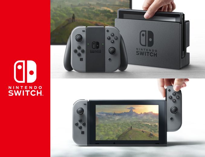
Playing with a launch-day Switch a bit, there's not much testing we can do since the console is so locked down. But one area where I've had some success is on power consumption testing. This is also an area where the Switch is a bit of an odd duck, leading to some confusion around the Web judging from some of the comment posts I’ve seen elsewhere. USB Type-C has been shipping in devices for a couple of years now, so it’s hardly a new standard, but given the slow upgrade cycle of PCs and smartphones it still isn’t an interface that the majority of consumers out there have dealt with. Furthermore due to its use case as a game console, the Switch is unlike any other USB Type-C device out there (more on this in a second). So I opted to spend some time profiling the device’s power consumption, in order to shed some light on what to expect.
More...
-
03-07-17, 08:06 AM #6773
Anandtech: How To Get Ryzen Working on Windows 7 x64
Officially, AMD does not support Ryzen CPUs on Windows 7. Given that Microsoft has essentially ended support for the OS, this is the type of response we expect from AMD – Intel has also stopped officially supporting Windows 7 on the newest platforms as well. 'Official' is a general term: some special customers may receive extended lifetime support, or drivers currently out in the ecosystem still work on the platforms. Official support refers to driver updates and perhaps security updates, but there’s nothing to stop you trying to install an OS to either system or platform.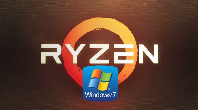
For clarification, we did not converse with AMD in writing this piece. AMD's formal position on Windows 7 on Ryzen is that it is unsupported, and as a result this means they will not provide support around it. There may also be other methods to install an unsupported OS, however here are a few solutions.
The Main Issue: USB Support
For installing Windows 7, the issues typically revolve around USB support. When there’s a mouse/keyboard plugged in, everything else after that is typically simple to configure (installing drivers, etc). However, from the 100-series chipsets on Intel and the AM4 motherboards on AMD, this can be an issue. When the CD or USB stick is being used to install the OS, the image needs USB drivers in order to activate a mouse or keyboard to navigate the install menus. This is the primary process that fails on both platforms and acts as a barrier to installation.
General Solution: Use a PS/2 Keyboard, if the motherboard has a PS/2 port
By default, on most systems, the way to guarantee the presence of a mouse pointer or keyboard activity during installation is to hook up a PS/2 keyboard. I’ve never known an installation to fail to recognize a PS/2 peripheral, so this is often the best bet. However, PS/2 as a connectivity standard is near dead (sometimes new keyboards will offer dual connectivity, like one of my Rosewill mechanical keyboards), with fewer motherboards supporting it, and it falls to USB as a backup.
The main reason why PS/2 should work where USB doesn’t is due to the protocol. PS/2 uses interrupts through the system, compared to USB which is based on polling. This results in different levels of engagement: the PS/2 keyboard injects its commands, but this means a lack of n-key rollover support, whereas a USB keyboard will bundle its commands up and send it over when the system requests it. Unfortunately, the latter requires a default driver to be able to do this.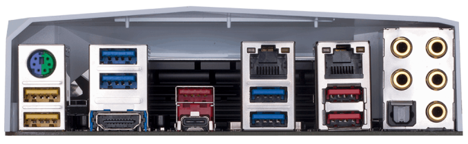
GIGABYTE AX370 Gaming 5 with a PS/2 Port
(As a general rule, always use USB 2.0 ports. These are most likely to be natively supported over USB 3.0 which can require chipset drivers.)
The problems facing users wishing to install Windows 7 who do not have a PS/2 port or peripherals come in two forms:
Problem 1: Installing Windows 7
With Intel on the Z170 series and above, it was a case of the USB 2.0 needing to be emulated through a BIOS option in order to install Windows 7, due to the EHCI support being removed. After a couple of weeks when motherboard manufacturers started rolling out BIOS/EFI updates to each of their products and enabling the option allowed users to have a keyboard during a standard install.
However, from personal experience, this only really worked when installing Window 7 from a CD, never from a USB stick. Somehow using a data-based USB stick would nullify having a mouse/keyboard via USB in the installation.
With AMD, it gets a little tricky. There is no EHCI emulation. But apparently this comes down to where the USB ports come from.
Potential Install Solution 1.1: Use a Chipset USB 2.0 Port
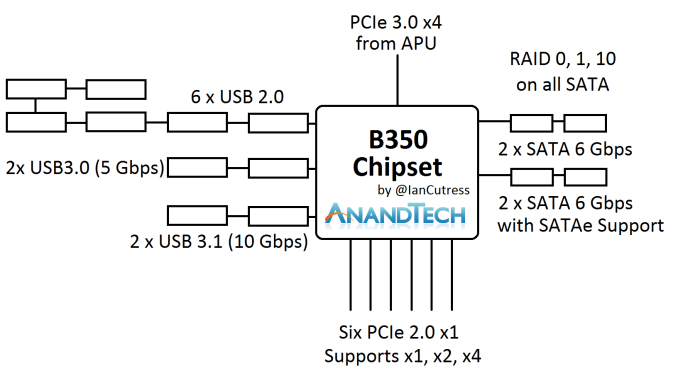
According to some documents obtained by AnandTech, the AMD BIOS treats USB ports from the CPU (because the CPU is an SoC) and USB ports from the 300-series chipset differently. From what we’ve seen, USB support is enabled on the chipset ports, but not on the CPU-based ports. Ryzen is a little different to previous desktop platforms because it can have USB ports from both. For example, here’s a CPU layout from Bristol Ridge and the B350 chipset, each showing USB ports.
The USB ports from the chipset are supposed to be natively supported in Windows 7 installation, allowing users to have access during either an OS install via USB or via a CD. But finding which ports on your device are supported via the chipset rather than the CPU can be tricky, especially if the motherboard manufacturer does not provide a block diagram of the onboard pathways and controllers. There’s also the fact that the onboard headers might be the ones based on the chipset, requiring header-to-port cabling to use.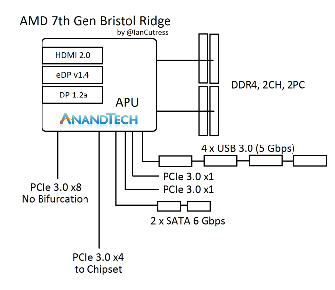
However, on my Crosshair VI Hero, this method as described in the documents, did not work. It may work on other boards, but not here.
Even if it did work, there may be a larger problem when it comes to accessing the OS, as explained further down.
Potential Install Solution 1.2: Use an Unattended Windows 7 Install
For users that customize their operating system packages, using tools available online, an unattended install usually covers this whole scenario. By being unattended, as long as no additional input is needed, it should sail straight through. Of course, this method usually means that the drive you want to use is ready to be used (with appropriate settings and partitioning). Power users familiar with this method will be comfortable here.
Potential Install Solution 1.3: Install Windows 7 on a Different System First
In our initial Ryzen review, in order to get SYSMark numbers comparable to the ones in our database, this is the method I had to use. In order to do so, we had to bend one of our more steadfast rules.
As a general thing to note, installing a Windows-based OS on one system and transferring the drive to another system is a bad idea. As part of the installation, Windows will detect what system is being used and install the base drivers for that system, for that CPU, and for that chipset. This provides clutter and confusion when moving the drive to another system, which is why we typically suggest that a new system gets a fresh OS install to help with this. While it’s still a bad idea, a fresh operating system is easier to manage than a fully-laden, well-used OS.
So for this method for our review, due to the timing of events, I had access to a Sandy Bridge system. I did a base install of Windows 7 x64 Professional using a USB stick on the Z77 motherboard with an R7 240 graphics card, and when the OS was loaded, did not install any extra drivers.
But, there lies a second issue.
Problem 2: USB Drivers on Windows 7
The 300-series based chipsets are identical to those offered by Bristol Ridge, and in part based on the Carrizo hardware, and as a result the Windows 7 drivers for these platforms work with AM4 for the main chipset support. Audio and Network drivers are a slightly different kettle of fish, and you may have to go hunting for the Windows 7 variants of these.
If you installed Windows 7 via a PS/2 keyboard and mouse, the OS should have access to the hardware and installing drivers should be easy.
The drivers that worked on launch day are the Crimson ReLive 17.2.1 Chipset Drivers, dated March 3rd. The following links are for the 64-bit versions.
- Most Up-to-Date: Chipset
- Previous Versions: http://support.amd.com/en-us/downloa...%2010%20-%2064
However, the USB fall back methods of 1.2 and 1.3 above do not account for actually having USB drivers in Windows 7 for Ryzen. Windows 7 may apply some base driver, which will allow users to access the hardware, but this is not guaranteed. There is a sure-fire method for doing this.
Windows 7 USB Driver Install 2.1: Integrate Drivers In The Unattended Install
For a power user that is familiar with adding installation packages or driver packages to their OS images, the following drivers extracted from the files above need to be:
- USB30_ZP\
- USB31_PT\
Rope this into your OS image and the USB ports will work. Otherwise...
Windows 7 USB Driver Install 2.2: Set Drivers To Install at Boot
This is the method I used to install the drivers. The basic premise is for the OS to install the drivers when the OS loads. All these actions need to take place on the secondary system that Windows 7 was installed on, aside from the last couple of instructions.
(Step 1) Download the ReLive 17.2.1 Chipset Drivers from the links above.
(Step 2) Run the Installer, but only to the point where it extracts the files and the Radeon screen comes up:
When this happens, go to where the drivers were extracted to, usually C:\AMD. Make a copy of this directory, wherever you need it to go, and exit the installer. The installer usually removes the original copy, and you can place it back into C:\AMD.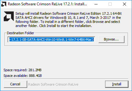
(Step 3) Go into the Radeon-Crimson-ReLive-17.2.1… directory and you will see the following: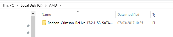
Now right click, and navigate to New -> Text Document: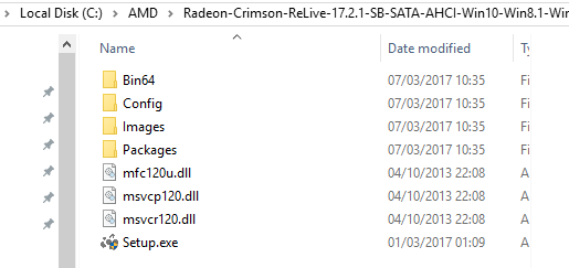
Select this, press enter to accept the default name, and open the file up. You should see an empty notepad file. In this, add the following: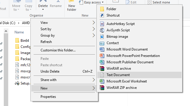
Setup.exe -installSave this file as ‘setup.bat’ in the same directory. You should see the following now in the setup folder: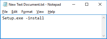
If the Setup file has the same icon as New Text Document, then the ‘.bat’ part of the filename did not work. You will need to go through Tools -> Options and enable ‘File Name Extensions’ in order to see the full file name and rename it this way to setup.bat (right click on the file, select rename).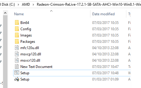
(Step 4) We now need to create a shortcut to this batch file in the Startup directory. From the start menu, go to ‘All Programs’, find the startup folder, right click and select ‘Open’.
It should offer an empty directory. Right-click, and select New -> New Shortcut, and a menu will popup. Select Browse, and navigate to the batch file (in this example, c:\AMD\Radeon-Crimson…).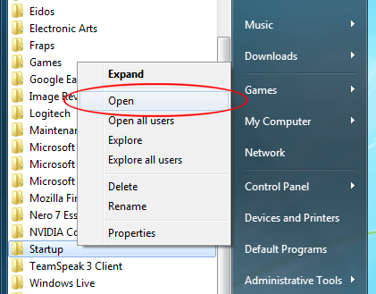
Select OK, the select next, and select finish. You should see the following in the directory: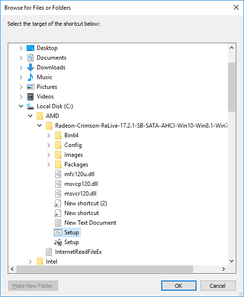
(Step 5) Shut down the system, and transfer the SSD over to the Ryzen system. Turn it on, and wait a few minutes after the system loads for the drivers to install. At some point, control of the mouse and keyboard will occur.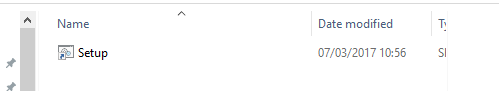
The TL;DR Flow Chart
For some of our power user readers that know how to extract files and create shortcuts, this flow chart might be easier to follow:
Limitations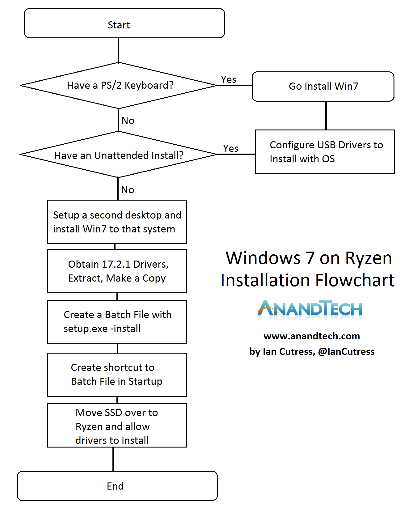
Arguably this solution could be ported to other circumstances where installing Windows 7 and not having USB is an issue. However, due to our limits in Ryzen testing, we’ve only tested this method, installing Win7 x64 Professional, on the Crosshair VI Hero so far. Other methods may work better as the platform evolves. However, it should still be stated that AMD is not officially supporting Ryzen and the AM4 platform on Windows 7.
Any users with other methods, or success/failure stories, please post below.
More...
-
03-07-17, 08:06 AM #6774
Anandtech: The Corsair Gaming K95 RGB Platinum Mechanical Keyboard Review
In this review we are having a look at the recently released Corsair Gaming K95 RGB Platinum, a mechanical gaming keyboard. It is a hybrid between the K70 RGB and K95 RGB models, with more features and a brand new CUE software package, designed to leave no gamer unsatisfied (for a price).
More...
-
03-07-17, 09:53 AM #6775
Anandtech: AMD Prepares 32-Core Naples CPUs for 1P and 2P Servers: Coming in Q2
For users keeping track of AMD’s rollout of its new Zen microarchitecture, stage one was the launch of Ryzen, its new desktop-oriented product line last week. Stage three is the APU launch, focusing mainly on mobile parts. In the middle is stage two, Naples, and arguably the meatier element to AMD’s Zen story.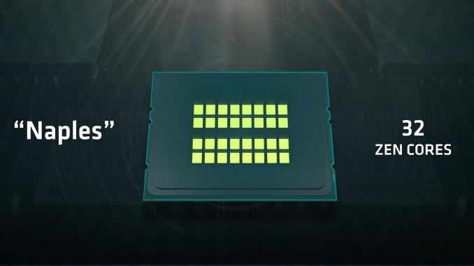
A lot of fuss has been made about Ryzen and Zen, with AMD’s re-launch back into high-performance x86. If you go by column inches, the consumer-focused Ryzen platform is the one most talked about and many would argue, the most important. In our interview with Dr. Lisa Su, CEO of AMD, the launch of Ryzen was a big hurdle in that journey. However, in the next sentence, Dr. Su lists Naples as another big hurdle, and if you decide to spend some time with one of the regular technology industry analysts, they will tell you that Naples is where AMD’s biggest chunk of the pie is. Enterprise is where the money is.
So while the consumer product line gets columns, the enterprise product line gets profits and high margins. Launching an enterprise product that gains even a few points of market share from the very large blue incumbent can implement billions of dollars to the bottom line, as well as provided some innovation as there are now two big players on the field. One could argue there are three players, if you consider ARM holds a few niche areas, however one of the big barriers to ARM adoption, aside from the lack of a high-performance single-core, is the transition from x86 to ARM instruction sets, requiring a rewrite of code. If AMD can rejoin and a big player in x86 enterprise, it puts a small stop on some of ARMs ambitions and aims to take a big enough chunk into Intel.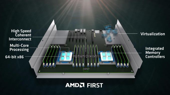
With today’s announcement, AMD is setting the scene for its upcoming Naples platform. Naples will not be the official name of the product line, and as we discussed with Dr. Su, Opteron one option being debated internally at AMD as the product name. Nonetheless, Naples builds on Ryzen, using the same core design but implementing it in a big way.
The top end Naples processor will have a total of 32 cores, with simultaneous multi-threading (SMT), to give a total of 64 threads. This will be paired with eight channels of DDR4 memory, up to two DIMMs per channel for a total of 16 DIMMs, and altogether a single CPU will support 128 PCIe 3.0 lanes. Naples also qualifies as a system-on-a-chip (SoC), with a measure of internal IO for storage, USB and other things, and thus may be offered without a chipset.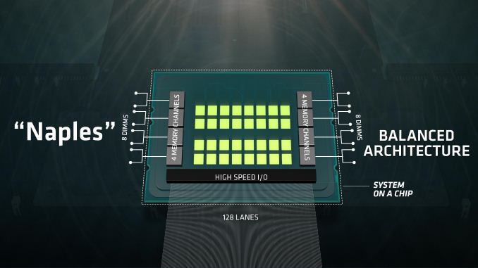
Naples will be offered as either a single processor platform (1P), or a dual processor platform (2P). In dual processor mode, and thus a system with 64 cores and 128 threads, each processor will use 64 of its PCIe lanes as a communication bus between the processors as part of AMD’s Infinity Fabric. The Infinity Fabric uses a custom protocol over these lanes, but bandwidth is designed to be on the order of PCIe. As each core uses 64 PCIe lanes to talk to the other, this allows each of the CPUs to give 64 lanes to the rest of the system, totaling 128 PCIe 3.0 again.
On the memory side, with eight channels and two DIMMs per channel, AMD is stating that they officially support up to 2TB of DRAM per socket, making 4TB in a single server. The total memory bandwidth available to a single CPU clocks in at 170 GB/s.
While not specifically mentioned in the announcement today, we do know that Naples is not a single monolithic die on the order of 500mm2 or up. Naples uses four of AMD’s Zeppelin dies (the Ryzen dies) in a single package. With each Zeppelin die coming in at 195.2mm2, if it were a monolithic die, that means a total of 780mm2 of silicon, and around 19.2 billion transistors – which is far bigger than anything Global Foundries has ever produced, let alone tried at 14nm. During our interview with Dr. Su, we postulated that multi-die packages would be the way forward on future process nodes given the difficulty of creating these large imposing dies, and the response from Dr. Su indicated that this was a prominent direction to go in.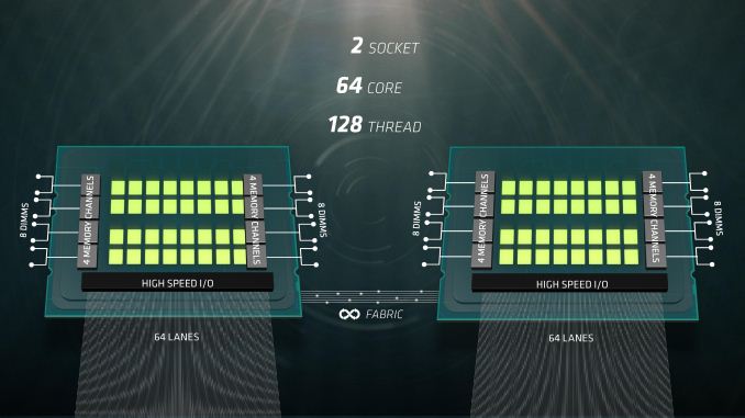
Each die provides two memory channels, which brings us up to eight channels in total. However, each die only has 16 PCIe 3.0 lanes (24 if you want to count PCH/NVMe), meaning that some form of mux/demux, PCIe switch, or accelerated interface is being used. This could be extra silicon on package, given AMD’s approach of a single die variant of its Zen design to this point.
Note that we’ve seen multi-die packages before in previous products from both AMD and Intel. Despite both companies playing with multi-die or 2.5D technology (AMD with Fury, Intel with EMIB), we are lead to believe that these CPUs are similar to previous multi-chip designs, however there is Infinity Fabric going through them. At what bandwidth, we do not know at this point. It is also pertinent to note that there is a lot of talk going around about the strength of AMD's Infinity Fabric, as well as how threads are manipulated within a silicon die itself, having two core complexes of four cores each. This is something we are investigating on the consumer side, but will likely be very relevant on the enterprise side as well.
In the land of benchmark numbers we can’t verify (yet), AMD showed demonstrations at the recent Ryzen Tech Day. The main demonstration was a sparse matrix calculation on a 3D-dataset for seismic analysis. In this test, solving a 15-diagonal matrix of 1 billion samples took 35 seconds on an Intel machine vs 18 seconds on an AMD machine (both machines using 44 cores and DDR4-1866). When allowed to use its full 64-cores and DDR4-2400 memory, AMD shaved another four seconds off. Again, we can’t verify these results, and it’s a single data point, but a diagonal matrix solver would be a suitable representation for an enterprise workload. We were told that the clock frequencies for each chip were at stock, however AMD did say that the Naples clocks were not yet finalized.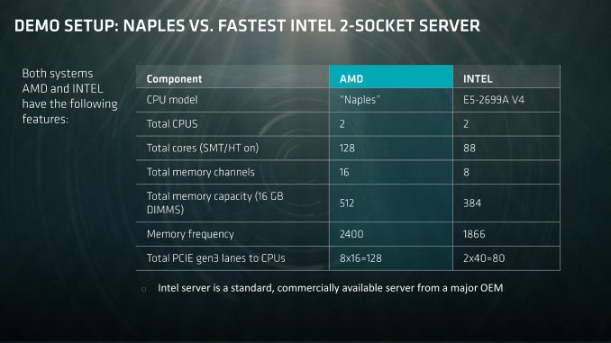
What we don’t know are power numbers, frequencies, processor lists, pricing, partners, segmentation, and all the meaty stuff. We expect AMD to offer a strong attack on the 1P/2P server markets, which is where 99% of the enterprise is focused, particularly where high-performance virtualization is needed, or storage. How Naples migrates into the workstation space is an unknown, but I hope it does. We’re working with AMD to secure samples for Johan and me in advance of the Q2 launch.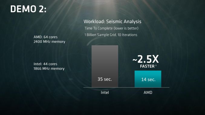
Gallery: AMD Naples Slide Deck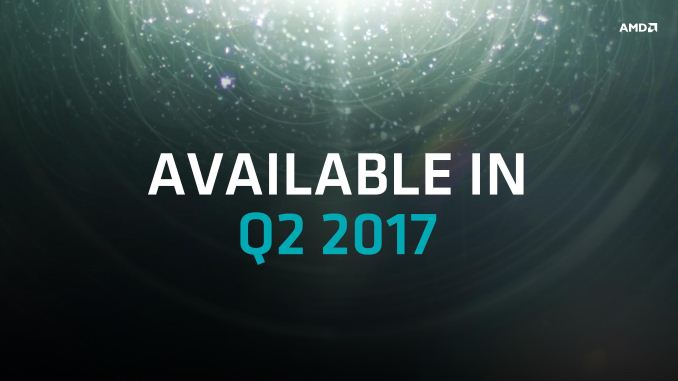


Related Reading- The AMD Zen and Ryzen 7 Review: A Deep Dive on 1800X, 1700X and 1700
- Making AMD Tick: A Very Zen Interview with Dr. Lisa Su, CEO
More...
- The AMD Zen and Ryzen 7 Review: A Deep Dive on 1800X, 1700X and 1700
-
03-07-17, 08:18 PM #6776
Anandtech: NVIDIA Announces Jetson TX2: Parker Comes To NVIDIAs Embedded System Kit
For a few years now, NVIDIA has been offering their line of Jetson embedded system kits. Originally launched using Tegra K1 in 2014, the first Jetson was designed to be a dev kit for groups looking to build their own Tegra-based devices from scratch. Instead, what NVIDIA surprisingly found, was that groups would use the Jetson board as-is instead and build their devices around that. This unexpected market led NVIDIA to pivot a bit on what Jetson would be, resulting in the second-generation Jetson TX1, a proper embedded system board that can be used for both development purposes and production devices.
This relaunched Jetson came at an interesting time for NVIDIA, which was right when their fortunes in neural networking/deep learning took off in earnest. Though the Jetson TX1 and underlying Tegra X1 SoC lack the power needed for high-performance use cases – these are after all based on an SoC designed for mobile applications – they have enough power for lower-performance inferencing. As a result, the Jetson TX1 has become an important part of NVIDIA’s neural networking triad, offering their GPU architecture and its various benefits for devices doing inferencing at the “edge” of a system.
Now about a year and a half after the launch of the Jetson TX1, NVIDIA is going to be giving the Jetson platform a significant update in the form of the Jetson TX2. This updated Jetson is not as radical a change as the TX1 before it was – NVIDIA seems to have found a good place in terms of form factor and the platform’s core feature set – but NVIDIA is looking to take what worked with TX1 and further ramp up the performance of the platform.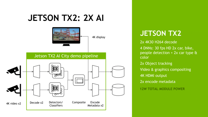
The big change here is the upgrade to NVIDIA’s newest-generation Parker SoC. While Parker never made it into third-party mobile designs, NVIDIA has been leveraging it internally for the Drive system and other projects, and now it will finally become the heart of the Jetson platform as well. Relative to the Tegra X1 in the previous Jetson, Parker is a bigger and better version of the SoC. The GPU architecture is upgraded to NVIDIA’s latest-generation Pascal architecture, and on the CPU side NVIDIA adds a pair of Denver 2 CPU cores to the existing quad-core Cortex-A57 cluster. Equally important, Parker finally goes back to a 128-bit memory bus, greatly boosting the memory bandwidth available to the SoC. The resulting SoC is fabbed on TSMC’s 16nm FinFET process, giving NVIDIA a much-needed improvement in power efficiency.
Paired with Parker on the Jetson TX2 as supporting hardware is 8GB of LPDDR4-3600 DRAM, a 32GB eMMC flash module, a 2x2 802.11ac + Bluetooth wireless radio, and a Gigabit Ethernet controller. The resulting board is still 50mm x 87mm in size, with NVIDIA intending it to be drop-in compatible with Jetson TX1.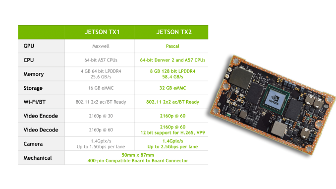
Given these upgrades to the core hardware, unsurprisingly NVIDIA’s primary marketing angle with the Jetson TX2 is on its performance relative to the TX1. In a bit of a departure from the TX1, NVIDIA is canonizing two performance modes on the TX2: Max-Q and Max-P. Max-Q is the company’s name for TX2’s energy efficiency mode; at 7.5W, this mode clocks the Parker SoC for efficiency over performance – essentially placing it right before the bend in the power/performance curve – with NVIDIA claiming that this mode offers 2x the energy efficiency of the Jetson TX1. As the TX1 was a 10W part, the gains in energy efficiency come from a mix of performance increases and the reduction in power consumption.
Meanwhile the board’s Max-P mode is its maximum performance mode. In this mode NVIDIA sets the board TDP to 15W, allowing the TX2 to hit higher performance at the cost of some energy efficiency. NVIDIA claims that Max-P offers up to 2x the performance of the Jetson TX1, which means NVIDIA has doubled performance for a roughly 50% increase in power consumption over the TX1.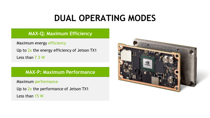
In terms of clockspeeds NVIDIA isn’t making those a front-and-center specification, but the numbers I’ve been quoted are 2GHz for the Denver 2 cores, 2GHz+ for the Cortex-A57 cores, and 1300MHz for the GPU. I suspect these numbers are for Max-Q mode – particularly as this would best line-up with NVIDIA’s 2x energy efficiency claims – but it’s not perfectly clear at this time.
Finally, along with announcing the Jetson TX2 module itself, NVIDIA is also announcing a Jetson TX2 development kit. The dev kit will actually ship first – it ships next week in the US and Europe, with other regions in April – and contains a TX2 module along with a carrier board to provide I/O breakout and interfaces to various features such as the USB, HDMI, and Ethernet. Judging from the pictures NVIDIA has sent over, the TX2 carrier board is very similar (if not identical) to the TX1 carrier board, so like the TX2 itself is should be familiar to existing Jetson developers.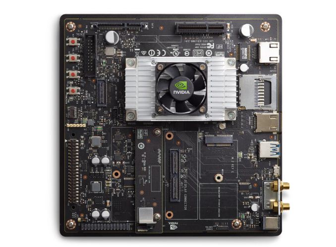
With the dev kit leading the charge for Jetson TX2, NVIDIA will be selling it for $599 retail/$299 education, the same price the Jetson TX1 dev kit launched at back in 2015. Meanwhile the stand-alone Jetson TX2 module will be arriving in Q2’17, priced at $399 in 1K unit quantities. In the case of the module, this means prices have gone up a bit since the last generation; the TX2 is hitting the market at $100 higher than where the TX1 launched.
More...
-
03-08-17, 07:05 AM #6777
Anandtech: Everspin Announces New MRAM Products And Partnerships
Magnetoresistive RAM manufacturer Everspin has announced their first MRAM-based storage products and issued two other press releases about recent accomplishments. Until now, Everspin's business model has been to sell discrete MRAM components, but they're introducing a NVMe SSD based on their MRAM. Everspin's MRAM is one of the highest-performing and most durable non-volatile memory technologies on the market today, but its density and capacity falls far short of NAND flash, 3D XPoint, and even DRAM. As a result, use of MRAM has largely been confined to embedded systems and industrial computing that need consistent performance and high reliability, but have very modest capacity requirements. MRAM has also seen some use as a non-volatile cache or configuration memory in some storage array controllers. The new nvNITRO family of MRAM drives is intended to be used as a storage accelerator: a high-IOPS low-latency write cache or transaction log, with performance exceeding that of any single-controller drive based on NAND flash.
Everspin's current generation of spin-torque MRAM has a capacity of 256Mb per die with a DDR3 interface (albeit with very different timings from JEDEC standard for DRAM). The initial nvNITRO products will use 32 or 64 MRAM chips to offer capacities of 1GB or 2GB on a PCIe 3 x8 card. MRAM has high enough endurance that the nvNITRO does not need to perform any wear leveling, which allows for a drastically simpler controller design and means performance does not degrade over time or as the drive is filled up—the nvNITRO does not need any large spare area or overprovisioning. Read and write performance are also nearly identical, while flash memory suffers from much slower writes than reads, which forces flash-based SSDs to buffer and combine writes in order to offer good performance. Everspin did not have complete performance specifications available at time of writing, but the numbers they did offer are very impressive: 6µs overall latency for 4kB transfers (compared to 20µs for the Intel SSD DC P3700), and 1.5M IOPS (4kB) at QD32 (compared to 1.2M IOPS read/200k IOPS write for the HGST Ultrastar SN260). The nvNITRO does rely somewhat on higher queue depths to deliver full performance, but it is still able to deliver over 1M IOPS at QD16, around 800k IOPS at QD8, and QD1 performance is around 175k IOPS read/150k IOPS write. MRAM supports fine-grained access, so the nvNITRO performs well even with small transfer sizes: Everspin has hit 2.2M IOPS for 512B transfers, although that is not an official performance specification or measurement from the final product.
As part of today's announcements, Everspin is introducing MRAM support for Xilinx UltraScale FPGAs in the form of scripts for Xilinx's Memory Interface Generator tool. This will allow customers to integrate MRAM into their designs as easily as they would use SDRAM or SRAM. The nvNITRO drives are a demonstration of this capability, as the SSD controller is implemented on a Xilinx FPGA. The FPGA provides the PCIe upstream link as a standard feature, the memory controller is Everspin's new and Everspin has developed a custom NVMe implementation to take advantage of the low latency and simple management afforded by MRAM. Everspin claims a 30% performance advantage over an unspecified NVRAM drive based on battery-backed DRAM, and attributes it primarily to their lightweight NVMe protocol implementation. In addition to NVMe, the nvNITRO can be configured to allow all or part of the memory to be directly accessible for memory-mapped IO, bypassing the protocol overhead of NVMe.
The initial version of the nvNITRO is built with an off-the-shelf FPGA development board and mounts the MRAM on a pair of SO-DIMMs. Later this year Everspin will introduce new denser versions on a custom PCIe card, as well as M.2 drives and 2.5" U.2 using a 15mm height to accommodate two stacked PCBs. By the end of the year, Everspin will be shipping their next generation 1Gb ST-MRAM with a DDR4 interface, and the nvNITRO will use that to expand to capacities of up to 16GB in the PCIe half-height half-length card form factor, 8GB in 2.5" U.2, and at least 512MB for M.2.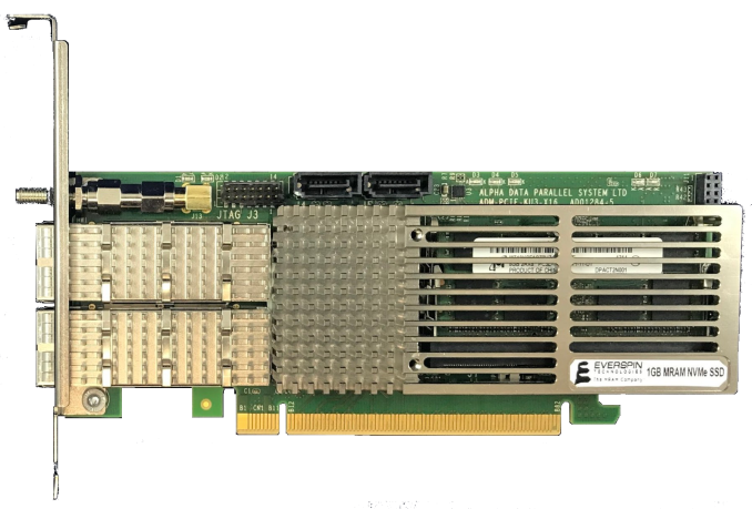
Everspin has not announced pricing for the nvNITRO products. The first generation nvNITRO products are currently sampling to select customers and will be for sale in the second quarter of this year, primarily through storage vendors and system integrators as a pre-installed option.
New Design Win For Current MRAM
Everspin is also announcing another design win for their older field-switched MRAM technology. JAG Jakob Ltd is adopting Everspin's 16Mb MRAM parts for their PdiCS process control systems, with MRAM serving as both working memory and code storage. These systems have extremely strict uptime requirements, hard realtime performance requirements and service lifetimes of up to 20 years; there are very few memory technologies on the market that can satisfy all of those requirements. Everspin will continue to develop their line of MRAM devices that compete against SRAM and NOR flash even as their higher-capacity offerings adopt DRAM-like interfaces.
More...
-
03-08-17, 07:50 AM #6778
Anandtech: The Western Digital Black PCIe SSD (512GB) Review
After acquiring SanDisk and introducing WD Green and WD Blue SSDs, it is no surprise to see Western Digital introduce a WD Black SSD that is a M.2 PCIe drive. Western Digital and SanDisk are relatively late to market with their first consumer PCIe SSD, but they've taken the time to refine the product. The WD Black PCIe SSD is an entry-level NVMe drive using TLC NAND and priced below the top SATA SSDs. It offers substantially better performance than the Intel SSD 600p for a modest price increase.
More...
-
03-08-17, 10:54 AM #6779
Anandtech: Imagination Announces PowerVR Furian GPU Architecture: The Next Generation
Taking place today is Imagination Technologies’ annual tech summit in Santa Clara, California. The company’s annual summit is always a venue for major Imagination news, and this year that’s particularly the case. As the cornerstone of this year’s summit, Imagination is announcing their next PowerVR GPU architecture: Furian.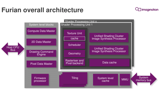
Furian marks the first new GPU architecture out of Imagination in almost 7 years. Rogue, the company’s first unified shader architecture, was first announced in 2010 and has become the cornerstone of Imagination’s entire GPU lineup, from wearables to high-end devices. In the intervening years, Imagination has made a number of smaller updates and optmizations to the architecture, leading to the 6, 7, and 8 series of PowerVR GPU designs. Now the company is undertaking a more radical revision to their architecture in the form of Furian, which like Rogue before it, will ultimately become the cornerstone of their GPU families.
I’ll have a deeper dive into Furian next week, but for today’s launch I want to hit the highlights of the new architecture and what Imagination’s goals are for the GPUs that will be derived from it. On that note, Imagination is not announcing any specific GPU designs today; while close partners already have beta RTL designs, the final designs and the announcement of those designs will come later in the year. But as the mobile industry is a bit more open in terms of design information due to the heavy use of IP licensing and the long design windows, it makes sense for Imagination to start talking this architecture up now, so that developers know what’s coming down the pipe.
Initially, Furian will co-exist alongside Rogue designs. The initial designs for Furian will be high-end designs, which means that Rogue will continue to cover customers’ needs for lower power and area efficient designs. In particular, the various XE designs will still be around for some time to come as Imagination’s leading design for area efficiency. XE will eventually be replaced by Furian, but this could potentially be some years down the line due to a mix of design priorities, cost, and the fact that new architecture features can hurt the area efficiency of a design.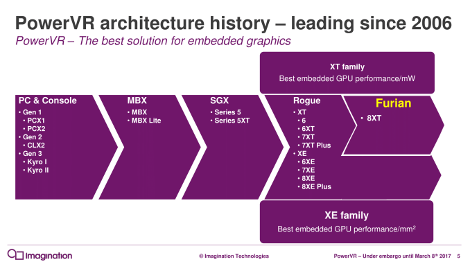
The ultimate goal of Furian is of course to improve power and performance, both on an energy efficiency (perf-per-milliwatt) and area efficiency (perf-per-mm2) basis. In fact it’s interesting that despite the fact that the first Furian designs will be high-end designs, Imagination is still first and foremost promoting area efficiency with Furian. Compared to a similarly sized and clocked Series7XT Plus (Rogue), Imagination is stating that a Furian design would offer 35% better shader performance and 80% better fill rate (though the company’s presentation doesn’t make it clear if this is texel or pixel), with an ultimate performance gain of a rather incredible 70-90%.
From an architectural standpoint Furian is not a new architecture designed from the ground-up, but rather is a rather significant advancement over what Imagination has already done with Rogue. We’re still looking at a Tile Based Deferred Rendering system of course – the bread and butter of Imagination’s GPU technology – with Imagination taking what they’ve learned from Rogue to significantly rework blocks at every level for better performance, greater capabilities, or better scaling. In fact the latter is a big point for the company, as this architecture ultimately needs to replace Rogue and last for a number of years, meaning a high degree of scalability is required. To do that, Imagination has essentially re-engineered their layout and data-flow for Furian – more hierarchical and less of a focus on a central hub – in order to ensure they can further scale up in future designs.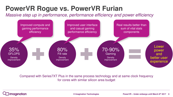
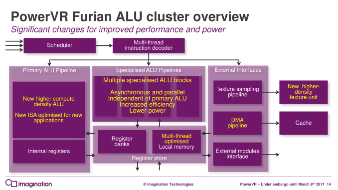 And as you’d expect for a new architecture, Imagination has made several changes under the hood at the ALU Cluster level – the heart of the GPU – in order to improve their GPU designs. The biggest change here – and I dare say most conventional – is that the company has significantly altered their ALU pipeline design. Whereas a full Rogue ALU would contain 16 pipelines per cluster, each composed of a number of ALUs of various sizes capable of issuing MADs (multiply + add), Furian takes things in a wider, less flexible direction.
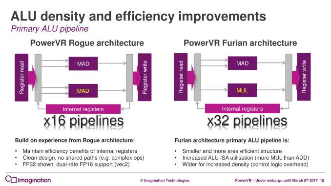
For Furian, a single pipeline drops the second MAD ALU for a simpler MUL ALU. This means that the ALUs in a pipeline are unbalanced – the ALUs aren’t equal in capability, and you need to come up with a MUL to fill the second ALU. The advantage of a pair of matching MAD ALUs is that the resulting architecture is conceptually clean and simple. The problem is that relative to simpler MUL or ADD ALUs, MAD ALUs are bigger, more power hungry, and put more pressure on the register file.
Ultimately Imagination found that they were having a hard time filling the second MAD on Rogue, and a MUL, while not as capable, could cover a lot of those use cases while being simpler. The net effect is that the second MUL will likely be used less than the MAD, but it will pay for itself in size and power.
Meanwhile as mentioned before, Imagination is also expanding the size of a cluster, from 16 pipelines to 32 pipelines. Rogue’s native wavefront size was 32 to begin with – executing half a wavefront over 2 cycles – so this isn’t as big a change as it first appears, since the actual thread granularity doesn’t change. However with one cluster for 32 pipelines instead of two clusters for 32 pipelines, this cuts down on the amount of control logic overhead. At the same time, presumably in anticipation of Furian designs having fewer clusters than comparable Rogue designs, Imagination has increased the performance of the texture unit, going from 4 bilinear samples/clock on Rogue to 8 bilinear samples/clock on Furian.
At a higher level, the compute capabilities of Furian will easily exceed those of Rogue. The architecture is designed to be OpenCL 2.x capable (conformance results pending), and there will be variations that are fully cache/memory coherent for heterogeneous processing. On that note, while it’s not outright HSA compliant, Furian adopts many of the hardware conventions of HSA, so it should behave like other heterogeneous solutions.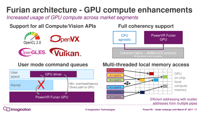
Though for more specialized workloads, in an interesting change Furian will be able to accommodate additional “function-specific” pipelines in customized GPU designs. How this is done is ultimately up to the customer – Imagination just provides the IP and reference RTLs – but the plumbing is there for customers to either add new functional hardware at the block level, or go as low level as the shader processor unit itself to add this hardware. The most obvious candidate here would be ray tracing hardware derived from Imagination’s Wizard architecture, but ultimately it’s up to the customers integrating the GPU IP and how much work they want to put in to add additional blocks.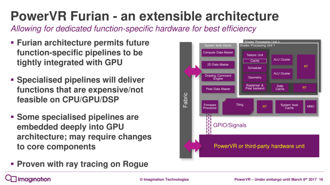
Finally, once Imagination is shipping final Furian designs, the company will be courting customers and downstream users in all of the major high-end markets for embedded GPUs. Besides the obvious high-end phones and GPUs where they’ll go head-to-head with the likes of ARM’s Bifrost architecture, Imagination will also be going after the automotive market, the VR market, and thanks to the compute improvements, the rapidly growing deep learning market. The nature of IP licensing means that end-users are a couple of layers down, so Imagination first needs to court direct customers to build SoCs tailored to these applications, but the capability is there in the IP should customers demand it.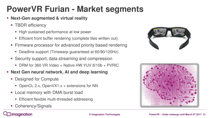
As for when we’ll see Furian designs in consumer hardware, that too is ultimately up to customers. Final Furian RTL designs will not be released to customers until sometime in the middle of this year, which is also why Imagination has not yet announced any specific GPU designs. As a result the lag time between announcement and implementation will be longer than past announcements, where the company was already announcing GPU designs with final RTL. Customers could potentially have Furian-equipped silicon ready towards the end of 2018 if they rush, but the bulk of the first-generation Furian products will likely be in 2019.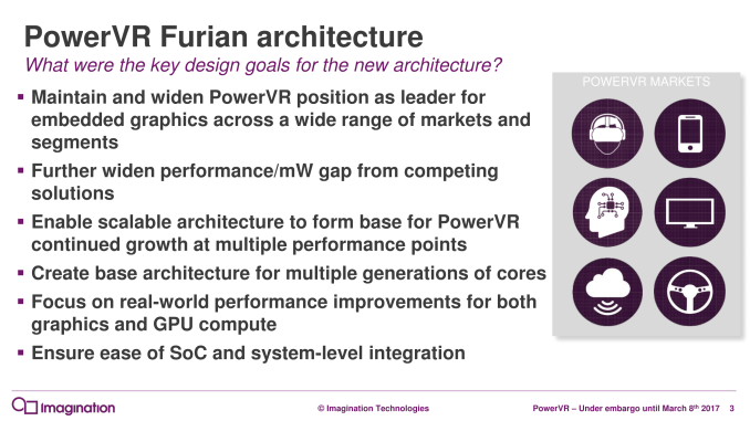
Gallery: PowerVR Furian Press Deck


More...
-
03-08-17, 09:43 PM #6780
Anandtech: Microsoft Details Project Olympus Open Compute Standard
Today, at the 2017 Open Compute Project U.S. Summit, Microsoft unveiled some significant announcements around their hyperscale cloud hardware design, which they first announced in November as Project Olympus. With the explosion of growth in cloud computing, Microsoft is hoping to reduce the costs of their Azure expansion by creating universal platforms in collaboration with the Open Compute Project. Project Olympus is more than just a server standard though. It consists of a universal motherboard, power supplies, 1U and 2U server chassis, power distribution, and more. Microsoft isn’t the first company to want to go down this road, and it makes a lot of sense to cut costs by creating standards when you are buying equipment on the level of Azure.
The company made several big announcements today, with the first one coming somewhat as a surprise, but when you read between the lines, it makes a lot of sense. Microsoft is partnering with Qualcomm and Cavium to bring ARM based servers to Azure. This is a pretty big shift for the company, since they have focused more on x86 computing, and changing to a new ISA is never a small task, so Microsoft is clearly serious about this move.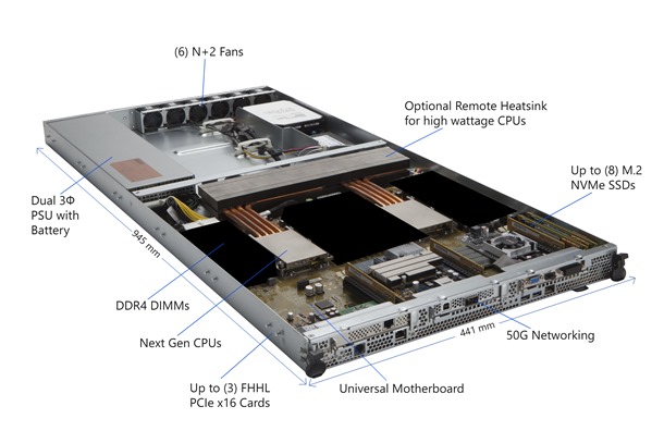
Microsoft Distinguished Engineer Leendert van Doorn expanded on why the company is exploring this option in a blog post today. Clearly ARM has made some progress in the server world over the last few years, and Microsoft feels it’s the right time to bring some of that capability to their own datacenters. I think one of the key takeaways is that Microsoft wants to shape the hardware capabilities to the workload, and with an open platform like ARM, this can make a lot of sense for certain workloads. He points out that search and indexing, storage, databases, big data, and machine learning, are all named as potential workloads, and in cloud computing, these are all significant in their own right.
Microsoft already has a version of Windows Server running on ARM, and they’ve announced that both of their partners will be demonstrating this internal use port of Windows Server, first with Qualcomm with their Centriq 2400 processor, with 48 cores on Samsung’s 10nm FinFET process. Cavium will be running on their second generation ThunderX2 platform. Our own Johan De Gelas did a thorough investigation of the original ThunderX platform in June 2016 and it is certainly worth a read. The takeaways were that Cavium needed to do a lot of work on power management, and they had some big performance bottlenecks, so they offered inferior performance per watt compared to a Xeon D, but better than advertised single-threaded performance with SPEC 2006 results only 1/3 the Xeon results, rather than the 1/5 that was advertised. If Cavium has fixed some of the issues, especially power consumption, the new ThunderX2 might be a compelling solution for specific tasks.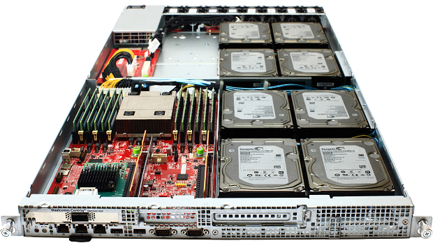 Qualcomm Centriq 2400 Platform
That is really the kicker though. The ARM platform, if properly executed, should be a good solution for some specific tasks, and if Microsoft can work with the platform makers to shape the hardware to fit specific tasks, but still be more general purpose than an ASIC, but at this time, it’s unlikely to be a serious threat to Intel’s monopoly on the datacenter at the moment. Intel has a pretty sizeable advantage in IPC, and especially on single-threaded workloads, so x86 isn’t going anywhere yet. What really matters is how Qualcomm and Cavium can execute on their platforms, and where they price them, since the end goal for Microsoft with this change is certainly, at least to some extent, to put pressure on Intel’s pricing for their datacenter equipment.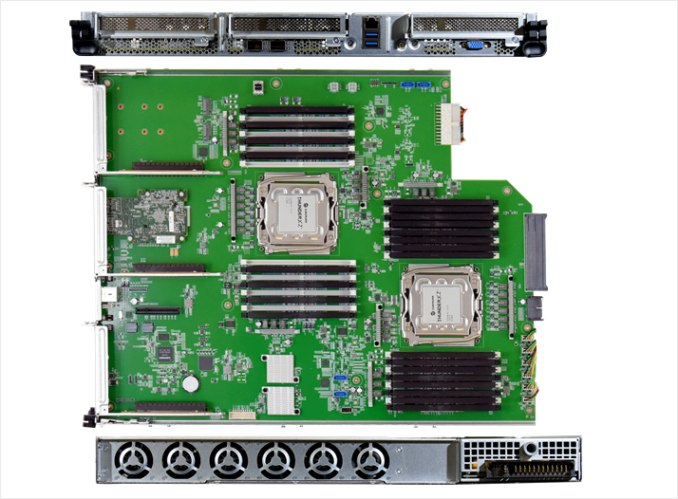 Cavium ThunderX2 Platform
Back on the x86 side, Microsoft also had some announcements there as well. AMD will also be collaborating with Microsoft to include their Naples processor into Project Olympus, which is their new server processor based on the “Zen” architecture. Although much of the news today has been around the ARM announcement, this is arguably the bigger play. Ryzen has already shown it is very competitive with Core, and Naples could be very strong competition for Xeon. We’ll have to wait for the launch to know for sure.
Microsoft didn’t abandon Intel either, and they announced close collaboration with Intel as well. This will be not only for Intel’s general purpose CPUs, but also for Intel’s FPGA accelerators and Nervana support. Microsoft already has FPGAs in Azure, so adding them to Project Olympus is a no-brainer.
Microsoft also announced a partnership with NVIDIA today, bringing the HGX-1 hyperscale GPU accelerator to Project Olympus. HGX-1 is targeted at AI cloud computing, which is certainly an area where there has been tremendous growth. Each HGX-1 will be powered by eight NVIDIA Tesla P100 GPUs, each with 3584 Stream Processors, based on the GP100 chip, and a new switching design based on NVIDIA NVLink and PCIe which allows a CPU to connect to any number of GPUs dynamically. NVIDIA states the HGX-1 provides up to 100x faster deep learning performance compared to CPU-based servers.
This is a pretty substantial update today for Project Olympus, and it looks to be an incredibly modular platform. Anyone reading that Microsoft is dropping Intel for ARM in Azure is misunderstanding this goal. Looking at the platform as a whole, it is abundantly clear that Microsoft wants a platform that can be designed to work with any workload, and still offer optimal performance, and efficiency. Some tasks will be best on ARM, some on x86, while GPUs will be leveraged for performance gains where possible, and FPGAs being utilized for other tasks. When you look at computing on the scale of something like Azure, it only makes sense to dedicate hardware to specific workloads, since you’ll certainly have enough different workloads to make the initial effort worthwhile, and that isn’t always the case when looking at small business, medium business, or even most enterprise workloads.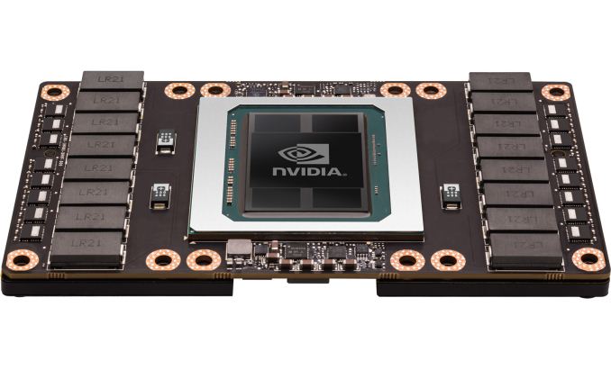
Source: Microsoft Azure Blog
More...


 Quote
QuoteThread Information
Users Browsing this Thread
There are currently 43 users browsing this thread. (0 members and 43 guests)


Bookmarks