

Results 6,831 to 6,840 of 12089
Thread: Anandtech News
-
04-03-17, 11:20 AM #6831
Anandtech: A New Challenger Appears: Palit's Own-Brand UVS and GFS SSDs Announced
Palit has announced two families of SSDs that it plans to sell under its own brand. The new drives are aimed at entry-level and mainstream gaming PCs, and will be based on controllers from Phison using 3D MLC or 3D TLC NAND flash memory from Micron depending on which drive you pick up. The Palit SSDs will be among the first drives on the market that will use a combination of a Phison controller and 3D NAND memory ICs from Micron, but we expect this combination to spread across several SSD vendors in due course.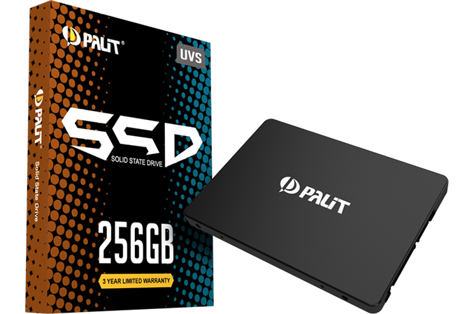
Palit Microsystems is one of the world’s largest producers of graphics cards, but it is not entirely new to SSDs too. Palit’s GALAX and KFA2 brands have offered Phison-based SSDs for quite a while, but their lineups have never been large and the whole effort looked more like a brand development rather than an attempt to compete against much of the market. This time, Palit has announced two families of SSDs under its own trademark and with seven drives in total, it plans to address entry-level and mainstream gaming PCs. We do not know Palit’s plans in regards of higher-end drives in M.2 or add-in-card form-factors, but such products are available from other brands that Palit owns and it should not be a problem for the company to expand its own lineup if it needs to.
Palit will initially offer two families of SSDs: First is the Palit UVS family, featuring the Phison S3111-S11 controller and 3D TLC memory for entry-level gaming systems. Then second is the Palit GFS family, based on the same Phison S3111-S11 controller but with 3D MLC NAND flash.
Before we start discussing the drives, let’s talk a little bit about the controller itself. Formally, the PS3111-S11 is positioned below the S10 because it has only two NAND channels with 16 CE targets and physically cannot deliver breakthrough performance. As it is a SATA controller, the PS3111-S11 does not have to deliver anything sequentially higher than 550 MB/s and this is something it can do with both MLC and TLC chips (sustained performance is a different comparison). The most important advancement of the controller versus its predecessors is that the PS3111-S11 supports LDPC ECC, and thus can be enabled on SSDs with sufficient endurance. Additionally, the PS3111-S11 supports 3D and 1z MLC/TLC NAND flash and memory with large (8 KB and 16 KB) blocks.Phison PS3111-S11 Controller Specifications PS3111-S11 Interface SATA 3.2 NAND Channels 2 CE Targets 16 DRAM Cache Supported ECC LDPC Supported Capacities MLC Up to 1 TB TLC 128 GB, 256 GB, 512 GB, 1 TB Supported NAND Toshiba 15 nm MLC/TLC
SK Hynix 14 nm MLC/TLC
Micron L06/B0KB
3D NAND
NAND flash memory with 8KB and 16KB blocks.Additional Features Data Compression
End to End Data Path Protection
As for the drives, the Palit UVS family will include 120 GB, 256 GB, 480 GB and 512 GB models using 3D TLC NAND (except the 120GB, which is planar TLC). Depending on the model, the drives are rated to deliver up to 560 MB/s sequential read speed and up to 470 MB/s (370 MB/s for the 120 GB version) sequential write speed. As for random performance, the numbers on the box give 72,500 read IOPS and up to 85,000 write IOPS.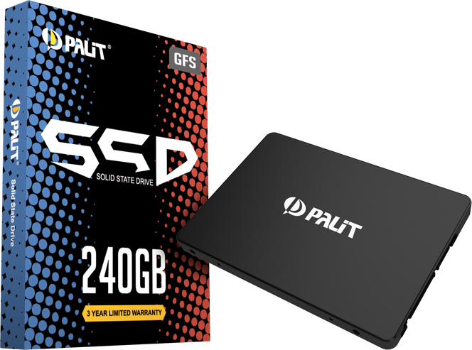
The Palit GFS lineup consists of three drives with 120 GB, 128 GB and 240 GB capacities all based on 3D MLC and offering all the endurance-related benefits of such memory. From a performance point of view, the GFS SSDs are slightly faster than the UVS drives: they are rated for up to 560 MB/s sequential read speed and up to 480 MB/s sequential write speed. Palit also states they can also perform up to 75,000 read IOPS and up to 87,500 write IOPS (240 GB version only). Palit may decide to expand the GFS lineup with higher-capacity offerings over time, but right now, its premium drives only offer entry-level capacities.
There are two intrigues about Palit’s SSDs: the memory supplier and actual manufacturer. Typically, Phison ships its controllers with memory and firmware and in many cases even provides assembly and test services (essentially, shipping already made drives). Despite this, Palit has enough SMT lines and can produce virtually everything itself. At present, we do not know whether Palit-branded SSDs are made by Palit, or are manufactured by a third party, but the latter is clearly a possibility here.Palit UVS and GFS SSDs Specifications UVS GFS UVS10AT-SSD120 UVS-SSD256 UVS-SSD480 UVS-SSD512 GFS-SSD120 GFS-SSD128 GFS-SSD240 Capacity 120 GB 256 GB 480 GB 512 GB 120 GB 128 GB 240 GB Controller Phison S3111-S11 NAND Flash TLC 3D TLC NAND 3D MLC NAND Sequential Read (max) 560 MB/s 525 MB/s 540 MB/s 560 MB/s Sequential Write (max) 375 MB/s 470 MB/s 465 MB/s 450 MB/s 480 MB/s Random Read IOPS (max) 70.0K 67.5K 72.5K 47.5K 75.0K Random Write IOPS (max) 77.5K 85K 87.5K DRAM Buffer 32 MB Pseudo-SLC Caching Supported Power Management DevSleep 5mW Form-Factor, Interface 2.5"/7 mm, Serial ATA 3.2 Warranty 3 years
The supplier of the NAND is also not obvious and could come from different sources. Palit does not disclose who is their supplier, but it is worth noting that Phison usually ships its controllers primarily with memory from Toshiba. We do know that there are Phison PS3111-S11-based reference designs featuring Toshiba’s BICS2 memory (which is not exactly positioned for SSDs by Toshiba) as well as S11 drives with Micron’s 3D NAND memory.
The Palit SSDs are expected to hit the market in the coming months. We do not have any information about their MSRP of the new drives, but it is logical to assume that Palit will try to make them competitive in terms of pricing.
Related Reading- CES 2016: Phison previews upcoming SSD controllers
- GALAX Shows Off Phison PS5008-E8 SSD with 3D NAND
- The Patriot Hellfire M.2 480GB Review: Phison NVMe Tested
- Corsair Gives Phison PS3110 S10 Another Try: Neutron XTi SSDs Launched
More...
-
04-04-17, 09:58 AM #6832
Anandtech: Apple to Redesign Mac Pro, Comments That GPU Cooling Was A Roadblock
In what’s turning out to be an oddly GPU-centric week for Apple, this morning the company has revealed that they will finally be giving the long-neglected Mac Pro a major update in the 2018+ timeframe. Apple’s pro users have been increasingly unhappy by the lack of updates to the company’s flagship desktop computer, and once released, this update would be its first in what will be over 4 years.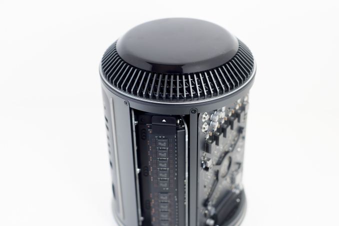
Getting to the heart of matters, Apple invited a small contingent of press – including John Gruber and TechCrunch’s Matthew Panzarino – out to one of their labs to discuss the future of the Mac Pro and pro users in general. The message out of Apple is an odd one: they acknowledge that they erred in both the design and handling of the Mac Pro (as much as Apple can make such an acknowledgement, at least), and that they will do better for the next Mac Pro. However that Mac Pro won’t be ready until 2018 or later, and in the meantime Apple still needs to assuage their pro users, to prove to them that they are still committed to the Mac desktop and still committed to professional use cases.
Both of these articles are very well written, and rather than regurgitate them, I’d encourage you to read them. It’s extremely rare to see Apple talk about their future plans – even if it’s a bit vague at times – so this underscores the seriousness of Apple’s situation. As John Gruber puts it, Apple has opted to “bite the bullet and tell the world what your plans are, even though it’s your decades-long tradition — a fundamental part of the company’s culture — to let actual shipping products, not promises of future products, tell your story.”
However neither story spends too much time on what I feel is the core technical issue, Apple’s GPU options, so I’d like to spill a bit of ink on the subject, if only to provide some context to Apple’s decisions.
Analysis: GPUs Find Their Sweet Spot at 250 Watts
From a GPU perspective, the Mac Pro has been an oddball device from day-one. When Apple launched it, they turned to long-time partner AMD to provide the GPUs for the machine. What AMD provided them with was their Graphics Core Next (GCN) 1.0 family of GPUs: Pitcairn and Tahiti. These chips were the basis of AMD’s Radeon HD 7800 and HD 7900 series cards launched in early 2012. And by the time the Mac Pro launched in late 2013, they were already somewhat outdated, with AMD’s newer Hawaii GPU (based on the revised GCN 1.1 architecture) having taken the lead a few months earlier.
Ultimately Apple got pinched by timing: they would need to have chips well in advance for R&D and production stockpiling, and that’s a problem for high-end GPU launches. These products just have slow ramp-ups.
Complicating matters is the fact that the Mac Pro is a complicated device. Apple favored space efficiency and low-noise over standard form-factors, so instead of using PC-standard PCIe video cards for the Mac Pro, they needed to design their own cards. And while the Mac Pro is modular to a degree, this ultimately meant that Apple would need to design a new such card for each generation of GPUs. This isn’t a daunting task, but it limits their flexibility in a way they weren’t limited with the previous tower-style Mac Pros.
The previous two items we’ve known to be issues since the launch of the Mac Pro, and have commonly been cited as potential issues holding back a significant GPU update all of these years. However, as it turns out, this is only half of the story. The rest of the story – the consequences of Apple’s decision to go with dual GPUs and using a shared heatsink via the thermal core – has only finally come together with Apple’s latest revelation.
At a high-level, Apple opted to go with a pair of GPUs in order to chase a rather specific use case: using one GPU to drive the display, and using the second GPU as a co-processor. All things considered this wasn’t (and still isn’t) a bad strategy, but the number of applications that can use such a setup are limited. Graphical tasks are hit & miss in their ability to make good use of a second GPU, and GPU-compute tasks still aren’t quite as prevalent as Apple would like.
The drawback to this strategy is that if you can’t use the second GPU, two GPUs aren’t as good as one more powerful GPU. So why didn’t Apple just offer a configuration with a single, higher power GPU? The answer turns out to be heat. Via TechCrunch:
I think we designed ourselves into a bit of a thermal corner, if you will. We designed a system that we thought with the kind of GPUs that at the time we thought we needed, and that we thought we could well serve with a two GPU architecture… that that was the thermal limit we needed, or the thermal capacity we needed. But workloads didn’t materialize to fit that as broadly as we hoped.The thermal core at the heart of the Mac Pro is designed to be able to cool a pair of moderately powerful GPUs – and let’s be clear here, at around 200 Watts each under full load, a pair of Tahitis adds up to a lot of heat – however it apparently wasn’t built to handle a single, more powerful GPU.
Being able to put larger single GPUs required a different system architecture and more thermal capacity than that system was designed to accommodate. And so it became fairly difficult to adjust.
The GPUs that have come to define the high-end market like AMD’s Hawaii at Fiji GPUs, or NVIDIA’s GM200 and GP102 GPUs, all push 250W+ in their highest performance configurations. This, apparently, is more than Apple’s thermal core can handle. In terms of total wattage, just one of these GPUs would be less than a pair of Tahitis, but it would be 250W+ over a relatively small surface area as opposed to the roughly 400W over nearly twice the surface area.
It’s a strange day when Apple has backed themselves into a corner on GPU performance. The company has been one of the biggest advocates for more powerful GPUs, pushing the envelope on their SoCs, while pressuring partners like Intel to release Iris Pro-equipped (eDRAM-backed) CPUs. However what Apple didn’t see coming, it would seem, is that the GPU market would settle on 250W or so as the sweet spot for high-end GPUs.Video Card Average Power Consumption (Full Load, Approximate) GPU Power Consumption AMD Tahiti (HD 7970) 200W AMD Hawaii (R9 290X) 275W AMD Fiji (R9 Fury X) 275W NVIDIA GM200 (GTX Titan X) 250W
And to be clear here, GPU power consumption is somewhat arbitrary. AMD’s Fiji GPU was the heart of the 275W R9 Fury X video card, but it was also the heart of the 175W R9 Nano. There is clearly room to scale down to power levels more in-line with Apple’s ability, but they lose performance in the process. Without the ability to cool a 250W video card, it’s not possible to have GPU performance that will rival powerful PC workstations, which Apple is still very much in competition with.
Ultimately I think it’s fair to say that this was a painful lesson for Apple, but hopefully one they learn a very important lesson from. The lack of explicit modularity and user-upgradable parts in the Mac Pro has always been a point of concern for some customers, and this has ultimately made the current design the first and last of its kind. Apple is indicating that the next Mac Pro will be much more modular, which would be getting them back on the right track.
More...
-
04-04-17, 09:58 AM #6833
Anandtech: ASUS Launches the Zen AiO ZN270IE: A 27-inch Full HD Core i7 All-In-One
ASUS has expanded its Zen AiO lineup of all-in-one PCs for 2017 with new 27” models. The company’s largest AIOs will fit into the current lineup of Intel Kaby Lake-based systems and offer bigger displays and higher performance than models featuring 22” and 24” screens due to desktop-class CPUs being installed.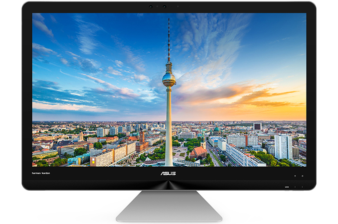
ASUS introduced its first AIO PCs with 22” and 24” monitors at Computex 2015 nearly two years ago. Since then the company has been gradually expanding its lineup of all-in-one desktop computers: first, it introduced more affordable Vivo AiO systems, and then it launched ASUS PRO AIOs for business users. Earlier this year the company began to add premium models into the Zen AiO family, targeting consumers who need better screens and/or higher performance. Back in January ASUS announced its Zen AiO Pro Z240IE, that is based on Intel’s 35W quad-core CPUs and 4K displays. In late March, ASUS added the Zen AiO ZN270IE into the lineup with a bigger 27” FHD display.
Just like the premium models introduced in January, the ASUS Zen AiO ZN270IE is based on Intel’s Core i7-T processors. However, similarities with the Zen AiO Pro Z240IE seem to end here. The Zen AiO ZN270IE comes with NVIDIA’s low-end GeForce 940MX GPU with 2 GB of DRAM (cheap versions of the ZN270IE use Intel’s iGPU, but this particular dGPU is barely faster than modern iGPUs), from 4 to 16 GB of DDR4 memory, up to a 512 GB SSD as well as 1 or 2 TB HDD storage, 802.11ac, a GbE controller and so on. The PC is equipped with an audio sub-system featuring four 3W speakers co-developed with harman/kardon, a 1 MP webcam (a premium version features Intel’s RealSense camera array with RGB and IR sensors), six USB Type-A ports, an SD/MMC card reader as well as HDMI connectors.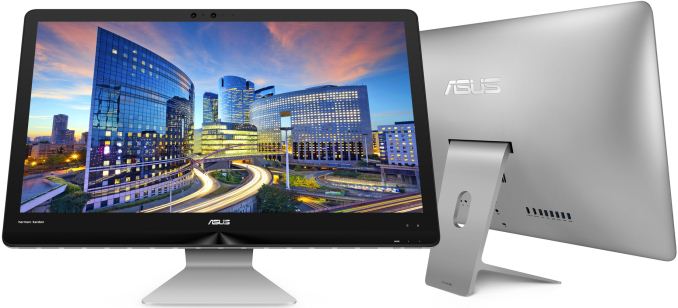
It is noteworthy that while ASUS now offers AIO PCs with 27” displays (some models will feature 10-point multi-touch, some will not), for now they still feature FHD resolution (1920×1080). Over time we may see more advanced 27” AIOs with higher-resolution screens and further performance enhancements, like Apple does with its iMac systems.ASUS 27" Zen AiO PC Specifications Zen AiO ZN270IE Display 27" IPS with 1920 × 1080 resolution
27" IPS with 1920 × 1080 resolution with 10-point multi-touchCPU Intel Core i7-7700T
4C/8T, 2.9/3.8 GHz
HD Graphics 630
35 WIntel Core i5-7400T
4C/4T, 2.4/3.0 GHz
HD Graphics 630
35 WPCH Intel H110 Graphics NVIDIA GeForce GTX 940MX 2GB (384 SPs)
Intel HD Graphics 630Memory 4 or 16 GB of DDR4 Storage 512 GB SSD (SATA or PCIe?)
1 or 2 TB 2.5" HDDWi-Fi IEEE 802.11ac Wi-Fi + BT 4.0 Ethernet GbE Display Outputs 1 × HDMI
1 × HDMI INAudio 4 × 3 W speakers (harman/kardon)
1 × audio in
1 × audio outUSB 4 × USB 3.0 Type-A (5 Gbps)
2 × USB 2.0 Type-AOther I/O 1 MP webcam
Intel RealSense cam (RGB and IR) on AIOs with multi-touch LCDs
SD/MMC card readerDimensions 649 mm × 481 mm × 62 mm PSU 90 W
120 WOS Windows 10 Home
ASUS has not announced recommended prices for its Zen AiO ZN270IE PCs, but since the company intends to offer multiple versions of the product, they will naturally vary significantly depending on the retailer/local distribution.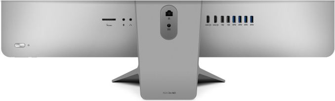
Gallery: ASUS Zen AiO ZN270IE


Related Reading:
- ASUS Designo Curve MX34VQ Incoming: 34" Ultrawide Curved Display with Qi Charging
- The Microsoft Surface Studio Review
- Microsoft Announces the Surface Studio: 28-inch AIO with Touch, Pen, 4500x3000, Skylake, GTX 980M
- CES 2016: 34-inch 3440x1440 AIO Hands-On at GIGABYTE
More...
-
04-04-17, 12:58 PM #6834
Anandtech: Transcend Launches New PCIe M.2 SSDs: The MTE850 Series
Transcend has announced its first SSDs based on 3D MLC NAND flash memory. The MTE850-series drives are aimed at the higher-end of the market and promise up to 2.5 GB/s sequential read speed along with endurance-related advantages of 3D NAND.
Transcend does not disclose exact specifications of all its new MTE850 series SSDs, but only shows their pictures as well as performance numbers for the flagship 512 GB model. The images reveal a controller covered with an aluminum heat spreader, and the only contemporary controller that supports 3D NAND and comes with such a heat spreader is Silicon Motion’s SM2260 (which uses two ARM Cortex cores and has eight NAND flash channels) Technically the SM2260 can support LDPC ECC technology and 256-bit AES although this has to be enabled in firmware. At present, only Micron sells SSD-graded 3D MLC NAND to some of its partners, so it is logical to assume that the MTE850 drives use Micron. Transcend is the third company to offer an SSD family featuring 3D MLC and SM2260 after ADATA and Mushkin, so the drives are going to have rivals that offer similar performance and functionality.
Transcend’s MTE850 family consists of three models with 128 GB, 256 GB and 512 GB capacities that come in M.2-2280 form-factor and use a PCIe 3.0 x4 interface. The manufacturer rates MTE850’s sequential read performance at up to 2.5 GB/s and its write performance at up to 1.1 GB/s when pseudo-SLC caching is used. When it comes to random performance, Transcend does not publish any numbers at all, but we know that the SM2260 controller is officially capable of up to 120K/140K 4KB read/write IOPS, although the final value for these drives will be firmware dependent.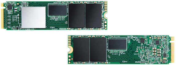
The MTE850 SSDs are expected to follow performance trends (the drives are somewhat comparable to Samsung’s 950 Pro released in 2H2015), and it is noteworthy that Transcend became the fourth independent SSD supplier after ADATA, Mushkin and Palit to introduce 3D NAND-based SSDs. We are still a few months away from a wide availability of 3D NAND-powered drives from independent vendors, but such products are getting announced today - we expect to hear more at Computex in June.Transcend MTE850 Specifications Capacity 128 GB 256 GB 512 GB Model Number TS128GMTE850 TS256GMTE850 TS512GMTE850 Controller Silicon Motion SM2260 NAND Flash 3D MLC NAND Form-Factor, Interface M.2-2280, PCIe 3.0 x4, NVMe 1.2 Sequential Read ? ? 2.5 GB/s Sequential Write ? ? 1.1 GB/s Random Read IOPS ? ? ? Random Write IOPS ? ? ? Pseudo-SLC Caching Supported DRAM Buffer Yes, capacity unknown TCG Opal Encryption No Power Management DevSleep, Slumber Warranty 3 years
Transcend did not disclose MSRPs for its MTE850 drives, but since the SSDs have direct competitors based on the same memory and controller (ADATA’s XPG SX8000-series at $90-$242), it is highly likely that Transcend’s SSDs will be offered at similar price points. The MTE850 drives will be covered by the manufacturer's three-year warranty.
Related Reading:
- Previewing Silicon Motion SM2260 NVMe Controller With 3D MLC NAND (512GB)
- Mushkin Announces Helix SSDs: 2.5 GB/s, 3D MLC NAND, SM2260, 2 TB Capacity
- ADATA Launches XPG SX8000: High-End M.2 NVMe SSD Featuring 3D MLC NAND
- Micron Cancels Ballistix TX3 NVMe SSD
More...
-
04-04-17, 03:22 PM #6835
Anandtech: ASUS Launches VG245Q 'Console' Gaming Monitor: 1080p with FreeSync, $200
ASUS has introduced another monitor positioned specifically for console gaming that allows console owners to take their games out of the living room. The new display offers Full-HD resolution and uses an inexpensive TN panel with a fast response time, supporting a refresh rate of 40Hz to 75Hz. It features AMD’s FreeSync technology as well as a DisplayPort port, so while this is aimed at more console type gaming, in order to use Freesync it essentially has to be a 'console' PC rather than an actual console.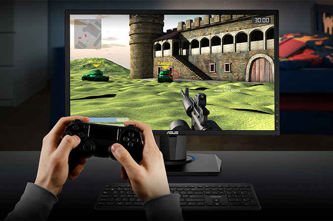
The ASUS VG245Q display uses a 24” TN panel with 1920×1080 resolution, and the general specifications are typical for budget devices: 250 nits brightness, 170°/160° viewing angles, a 1 ms response time (grey-to-grey) and so on. The monitor comes with two 2 W speakers and has two HDMI (so to connect to two consoles), one DisplayPort and one D-Sub connector. The VG245Q can adjust its height, swivel, and pivot. One of the important selling points of the ASUS VG245-series monitors is support for AMD’s FreeSync dynamic framerate technology that works at refresh rates ranging from 40 to 75 Hz.
In fact, ASUS’ VG245 family of displays, aimed at 'console' gaming, now includes three models: the VG245Q (introduced this month), the VG245H, and the VG245HE, with the latter two launched last fall. All the monitors use the same panel and have slightly different feature sets. The VG245H uses the same chassis as the VG245Q, but lacks DisplayPort. Meanwhile, the VG245HE is the most simplistic in the lineup, as it does not have swivel, pivot or height adjustments.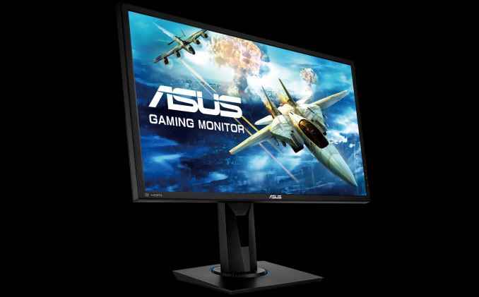
While ASUS formally positions its VG245-series displays as reasonably priced solutions for consoles, these devices are cheaper gaming monitors carrying the ASUS brand. They enable the company to address the entry-level segment of the PC market (keep in mind that the sRGB is supported as a feature of the ASUS GameVisual menu) without distracting attention of the masses from the higher-end models with advanced specs and features.ASUS VG245-Series Console Gaming Monitors ASUS
VG245H
(Added Adjust)ASUS
VG245HE
(Base Model)ASUS
VG245Q
(FreeSync)Panel 24" TN Native Resolution 1920 × 1080 Refresh Rate Range 75 Hz 75 Hz 40-75 Hz Response Time 1 ms (gray-to-gray) Brightness 250 cd/m² Contrast '100000000:1'
ASUS stupid smart contrast ratioViewing Angles 170°/160° horizontal/vertical Color Saturation 72% NTSC
sRGB mode availableInputs 2 × HDMI
1 × D-Sub2 × HDMI
1 × D-Sub
2 × DPAudio 2 × 2 W speakers
Audio in/out portsProprietary Enhancements Trace Free Technology
GamePlus Modes: Crosshair/Timer/Display Alignment
Low Blue Light: Yes
GameVisual Modes: Scenery/Racing/Cinema/RTS/RPG/FPS/sRGBMechanical Chassis Color Black Tilt +33°~-5° Swivel -90°~+90° - -90°~+90° Pivot +90°~-90° - +90°~-90° Height Adjustment 0~130 mm - 0~130 mm VESA Wall Mounting 100 × 100 mm Power Consumption Idle ~0.5 W Active 40 W Detailed Information Link Link Link
ASUS has not announced precise MSRP for its VG245Q monitor, but at present, the VG245H can be acquired for $179.99. It is unlikely that the addition of a DisplayPort connector significantly affected the cost of the VG245Q vs. the VG245H and it is logical to expect the two products to cost about the same.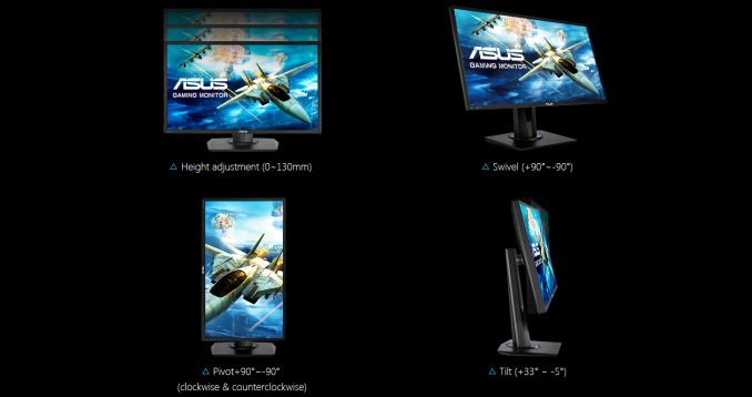
Gallery: ASUS VG245Q Console Gaming Monitor


Related Reading:
- ASUS Announces Three New Displays with Adaptive-Sync Technology
- ASUS VA326H and VA326N-W: 31.5-Inch Curved 144 Hz FHD Displays for $399
- ASUS Demonstrates ROG Swift PG27UQ: 4K, 144 Hz, HDR, DCI-P3 and G-Sync
More...
-
04-05-17, 06:18 AM #6836
Anandtech: Honor Announces The Honor 8 Pro: Kirin 960, 5.7-inch QHD
Today Honor is announcing the latest update to their product portfolio. After the successful launch of the Honor 8 last August as its flagship product, using the latest Kirin chipset back then, Honor is launching a higher-end model with a larger screen, more powerful SoC and an all-around upgrade.
The new device will have the newest Kirin 960 chipset, featuring 4x ARM Cortex-A73 and 4x ARM Cortex-A53 as well as the latest Mali-G71MP8 graphics, as we've seen on Huawei devices over the last six months. This will be paired with 6GB of LPDDR4 and 64GB of UFS 2.1 storage. The display moves up from the 5.2-inch Full-HD on the Honor 8 to a 5.7-inch QHD (2560x1440), and a combination of all these features means that Honor is promoting the Honor 8 Pro as a gaming and VR device, although there's no word on DayDream VR support, but the device will have some bundled VR software and support Google Cardboard. The display will target some form of DCI-P3, although the level of which has not been publicized as of yet.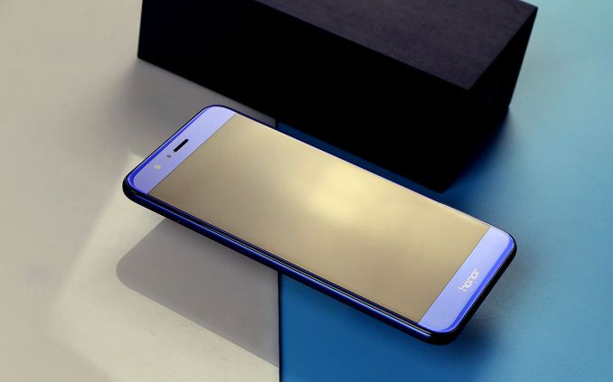
On the battery side, the larger device allows for a 4000 mAh battery. Similar to the Mate 9, this will support Huawei Supercharge with appropriate power adapters for faster charging via the Type-C port on the bottom of the phone. This is still a USB 2.0 port, as per the regular Honor 8.Honor 8 Series Honor 8 Pro
(April 2017)Honor 8
(August 2016)SoC HiSilicon Kirin 960
4x Cortex-A73 @ 2.36GHz
4x Cortex-A53 @ 1.84GHz
ARM Mali-G71MP8HiSilicon Kirin 950
4x Cortex-A72 @ 2.30GHz
4x Cortex-A53 @ 1.81GHz
ARM Mali-T880MP4 @ 900MHzDisplay 5.7-inch 2560x1440 IPS LCD 5.2-inch 1920x1080 IPS LCD Dimensions 157.0 x 77.5 x 6.97 mm
184 grams145.5 x 71.0 x 7.45 mm
153 gramsRAM 6GB LPDDR4 3GB / 4GB LPDDR4-2666 NAND 64GB (UFS 2.1)
+ microSD32GB / 64GB (eMMC)
+ microSDBattery 4000 mAh
non-replaceable3000 mAh (11.46 Wh)
non-replaceableFront Camera 8MP, f/2.0 8MP, 1.4μm, f/2.4 Rear Camera 2x 12MP (color + monochrome), 1/2.9” Sony IMX286 Exmor RS, 1.25µm pixels, f/2.2, Laser AF + depth, HDR, dual-tone LED flash 2x 12MP (color + monochrome), 1/2.9” Sony IMX286 Exmor RS, 1.25µm pixels, f/2.2, Laser AF + depth, HDR, dual-tone LED flash Modem HiSilicon LTE (Integrated)
2G / 3G / 4G LTE (Category 12/13)
FDD-LTE / TD-LTE / TD-SCDMA / WCDMA / GSMHiSilicon Balong (Integrated)
2G / 3G / 4G LTE (Category 6)
FDD-LTE / TD-LTE / TD-SCDMA / WCDMA / CDMA (China only) / GSMSIM Size 2x NanoSIM (w/o microSD)
(dual standby)2x NanoSIM (w/o microSD)
(dual standby)Wireless 802.11a/b/g/n/ac, BT 4.2 LE, NFC, GPS/GNSS 802.11a/b/g/n/ac, BT 4.2 LE, NFC, IrLED, GPS/GNSS Connectivity USB 2.0 Type-C, 3.5mm headset USB 2.0 Type-C, 3.5mm headset Launch OS Android 7.0 with Emotion UI 5.1 Android 6.0 with Emotion UI 4.1
The Honor 8 Pro uses the same dual-camera setup seen in the Honor 8, using a 12MP RGB and a 12MP monochrome sensor for additional contrast focus capabilities, depth sensing, and bokeh. Given the relationship between Huawei and the Honor brand internally, it might not be a surprise that the Honor 8 Pro doesn't have the second generation of dual camera design as seen in the Huawei P10 that was launched back in February - it is likely that the Honor 9 will use that when released later in the year (as follows typical Honor cadence). The move to EMUI 5.1 will afford some additional software adjustments with the camera, and one of the features Honor was keen to promote is 4K recording in H.265, as well as an embedded feature called Highlights (co-created with GoPro) to help merge relevant photos and clips taken with the device when the user has a specific journey.
Current plans have the Honor 8 Pro launching in Western Europe (so we assume that means UK, France, Germany, Italy, Spain) to begin with, at a recommended price of 549 Euro or £475 (including tax). The navy blue color from the original Honor 8 will carry forward, along with two other designs in gold or black, although color availability may be region dependent. Pre-orders are currently available at vmall.eu (Honor's EU storefront), or a full Amazon launch will occur on April 20th.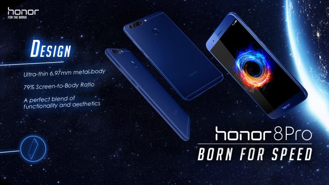
More...
-
04-05-17, 09:41 AM #6837
Anandtech: AMD Releases Radeon Software ReLive Crimson Edition 17.4.1
The game releases trickle this time of year, but the progression of technology marches on. More specifically VR is still a developing phenomenon, and 8K is just cresting the Horizon. Today’s AMD driver provides its fixes and steps us a little further along and prepares us for things to come.
This week’s AMD Radeon Software Crimson 17.4.1 release brings us Display Driver version 17.10.1061 (Windows Driver Store Version 22.19.156.1) and comes with multiple bug fixes, including a fix for Radeon Settings becoming unresponsive during a driver upgrade, a fix for display flicker when running windowed borderless applications on an AMD FreeSync display, and some improvement of Multi GPU scaling while playing Tom Clancy’s Ghost Recon Wildlands. Additionally, a sudden unplugging of AMD XConnect after installation of Radeon Software will no longer cause a system hang.
Meanwhile As the VR agenda continues to move forward, support for the ecosystem continues to improve. First on the list, this AMD driver release enables support for Oculus’ Asynchronous Spacewarp technology, the company's latest frame extrapolation feature, on more AMD cards. Async Spacewarp support launched on AMD's RX 400 series (Polaris) cards last year, and as of this driver update, the Radeon R9 Fury (Fiji), Radeon R9 390, and Radeon R9 290 series (Hawaii) cards have been added to the list. On a similar note, support for Valve's functionally similar SteamVR Asynchronous Reprojection technology has been added to AMD's drivers. However also like Spacewarp, AMD is starting slow in adding support for Reprojection; only the Radeon RX 480 and Radeon RX 470 cards on Windows 10 get support for Reprojection today.
On the video interface front, AMD has finally formally enabled DisplayPort 1.4 HBR3 support. The Polaris hardware has been able to support this feature since the start, however as displays are still catching up, AMD is only now finally enabling it. This opens display possibilities requiring much more bandwidth, and listed on the release notes are 8K 30Hz on a single cable and 8K 60Hz on two cables. 8K monitors are slim pickings right now but it’s great for video card vendors to be prepared.
As always, those interested in reading more or installing the updated hotfix drivers for AMD’s desktop, mobile, and integrated GPUs can find them either under the driver update section in Radeon Settings or on AMDs Radeon Software Crimson ReLive Edition download page.
More...
-
04-06-17, 08:17 AM #6838
Anandtech: Samsung Investing in 3840x1080 and 3840x1200 Curved Displays at 144 Hz
One of the interesting elements in the new wave of monitor technologies is the types of ideas that panel manufacturers are coming up with. In the enterprise space, custom display configurations occur more frequently than we might expect, but for consumers there tends to be a line of standardization. Samsung, being vertically integrated, gives them the opportunity to experiment more than most. Even then, as a reviewer in the industry, one develops certain expectations of what might be coming in the future. Consider me stumped, as TFTCentral has delved into Samsung’s upcoming roadmaps and panel production schedules to pull out one or two surprises.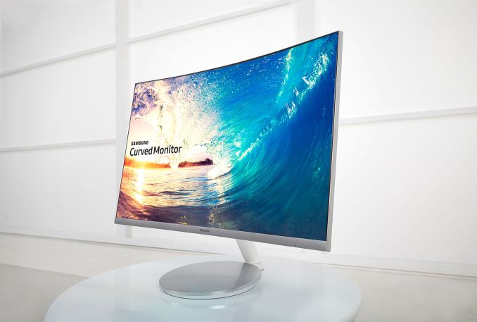
49-inch 3840x1080, or ‘Double Full-HD / DFHD’
For readers on the leading-edge of monitor configurations, ultra-wide displays in the 21:9 aspect ratio have been on the radar for about two years. These are monitors that have a 2560x1080 display, stretching the horizontal dimension of a standard 1920x1080 Full-HD monitor and make it easier to display modern cinema widescreen format content with less black bars. They are also claimed to assist with peripheral vision when gaming beyond a standard 1920x1080 display, or when curved, help with immersive content.
So chalk up some surprise when we hear that Samsung has an even wider format panel in the works. 3840x1080 represents a 32:9 aspect ratio, and the report states that this will be a VA panel with 1800R curvature and a 3-side frameless design. Putting that many pixels in a large display gives a relatively low 81.41 PPI. This panel will be part of Samsung’s ‘Grand Circle’ format, and by supporting up to 144 Hz it is expected that variants of this panel will be included with FreeSync/GSYNC technologies. One figure to note would be the contrast ratio – 5000:1 (static), which TFTCentral states is higher than current Samsung VA panels.
44-inch 3840x1200
This panel is the equivalent two 24.7-inch 1920x1200 screens put side-by-side, and indicates which market Samsung would be aiming for. The specifications seem to be almost identical to the 3840x1080 panel, such as 1800R curvature, but in a 29:9 aspect ratio with 60 Hz and 144 Hz variants. Pixel density is slightly higher than the other panel too, given the higher resolution and lower diagonal, which gives 91.41 PPI. TFTCentral is listing these panels as having an 8-bit color depth (no word on FRC), and likely to be qualified on some amount of sRGB. Other numbers, such as brightness and response time, are still unknown.
An amusing aside, for any users looking for a 16:10 display, something like two of these stacked on top of each other might be suitable (albeit massive) if these panels also offer a 3-side borderless configuration. I know Ryan has been after a decent 3840x2400 display, but given our discussions with monitor manufacturers, there seems to be no 16:10 demand from consumers.
So while these two panels aren’t official announcements (they don't even have official part numbers yet), and production will depend on how well these technologies scale. But by virtue of being on roadmaps and panel lists it is clear that Samsung has at least been doing research towards some wider aspect ratio displays. Information from TFTCentral is claiming mass production for both of these panels in September 2017, which means we might see some early announcements for retail-grade panels at Computex in June, or at IFA at the end of August with some pre-production run models. Full retail then might happen in the second half of the year, or along with further announcements at CES in January.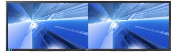
A bad mockup of two non-curved 16:10 displays
Related Reading- Dell’s 32-inch 8K UP3218K Display Now For Sale: Check Your Wallet
- HP Announces Omen X 35-Inch Curved Display for Gamers
- ASUS Designo Curve MX34VQ Incoming: 34" Ultrawide Curved Display
Gallery: Samsung Investing in 3840x1080 and 3840x1200 Curved Displays at 144 Hz

More...
-
04-06-17, 11:22 AM #6839
Anandtech: Microsofts Project Scorpio: More Hardware Details Revealed
This news piece contains speculation, and suggests silicon implementation based on released products and roadmaps. The only elements confirmed for Project Scorpio are the eight x86 cores, >6 TFLOPs, 320 GB/s, it's built by AMD, and it is coming in 2017. If anyone wants to officially correct any speculation, please get in touch.
One of the critical points of contention with consoles, especially when viewed through the lens of the PC enthusiast, is the hardware specifications. Consoles have long development processes, and are thus already behind the curve at launch – leading to a rapid expansion away from high-end components as the life-cycle of the console is anywhere from five to seven years. The trade-off is usually that the console is an optimized platform, particularly for software: performance is regular and it is much easier to optimize for.
For six months or so now, Microsoft has been teasing its next generation console. Aside from launching the Xbox One S as a minor mid-season revision to the Xbox One, the next-generation ‘Project Scorpio’ aims to be the most powerful console available. While this is a commendable aspiration (one that would look odd if it wasn’t achieved), the meat and potatoes of the hardware discussion has still been relatively unknown. Well, some of the details have come to the surface through a PR reveal with Eurogamer’s Digital Foundry.
We know the aim with Project Scorpio is to support 4K playback (4K UHD Blu-Ray), as well as a substantial part of 4K gaming. With recent introductions in the PC space of ‘VR’ capable hardware coming down in price, Microsoft is able to carefully navigate what hardware it can source. It is expected that this generation will still rely on AMD’s semi-custom foundry business, given that high-end consoles are now on x86 technologies and Intel’s custom foundry business is still in the process of being enabled (Intel’s custom foundry is also expected to be expensive). Of course, pairing an AMD CPU and AMD GPU would be the sensible choice here, with AMD launching a new GPU architecture last year in Polaris.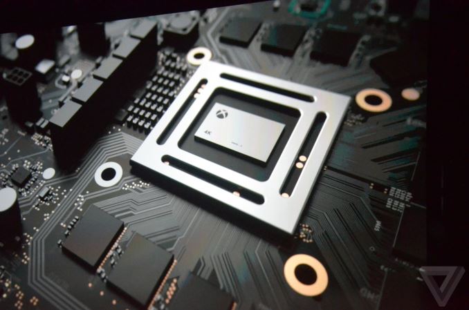
Here’s a table of what the reveal is:
Specifications in italics were added after the table was created.Microsoft Console Specification Comparison Xbox 360 Xbox One Project Scorpio CPU Cores/Threads 3/6 8/8 8 / ? CPU Frequency 3.2 GHz 1.6 GHz (est) 2.3 GHz CPU µArch IBM PowerPC AMD Jaguar AMD x86 ? Shared L2 Cache 1MB 2 x 2MB ?
GPU L2 is 4xGPU Cores 16 CUs
768 SPs
853 MHz40 CUs
1920 SPs ?
1172 MHzPeak Shader Throughput 0.24 TFLOPS 1.23 TFLOPS >6 TFLOPs Embedded Memory 10MB eDRAM 32MB eSRAM None Embedded Memory Bandwidth 32GB/s 102-204 GB/s None System Memory 512MB GDDR3-1400 8GB DDR3-2133 12GB GDDR5-1700 System Memory Bus 128-bits 256-bits 384-bit System Memory Bandwidth 22.4 GB/s 68.3 GB/s 326GB/s Manufacturing Process 28nm 16nm TSMC
At the high level, we have eight ‘custom’ x86 cores running at 2.3 GHz for the CPU and 40 compute units at 1172 MHz for the GPU. The GPU will be paired with 12GB of GDDR5, to give 326GB/s of bandwidth. Storage is via a 1TB HDD, and the optical drive supports 4K UHD Blu-Ray.
Let’s break this down with some explanation and predictions.
Eight Custom CPU Cores
The Xbox One uses AMD’s Jaguar cores – these are low powered and simpler cores, aimed at a low-performance profile and optimized for cost and power. In non-custom designs, we saw these CPUs hit above 2 GHz, but these were limited to 1.75 GHz in the Xbox One. While not completely impossible, it would be unlikely that Jaguar cores (that were made on a 28nm process) would also be in the Scorpio.
The other cores AMD has available are Excavator based (28nm) or Zen based (14nm). The latter is a design that has returned AMD to the high-end of x86 performance computing, offering high performance for reasonable power, but a 14nm design would be relatively expensive. Eight cores would fit in with a standard Zeppelin silicon design, which AMD has been manufacturing hand-over-fist since the launch of desktop-based Zen CPUs for PCs in March. One of the detractors against Zen inside Scorpio is the fact that it was only launched recently, and arguably the desktop PC market is more financially lucrative for AMD.
Technically Microsoft could go for Zen in the Scorpio, but I suspect this would increase the base cost of the console. However, if Microsoft were going for a premium console ($700+), this might make sense.
A note on Zen power and frequency – 2.3 GHz is a low frequency for a Zen CPU based on what we have seen in desktop PCs. Some work done internally on the power consumption of Zen CPUs has shown that the design requires a lot of power to move between 3.5 GHz and 4.0 GHz, perhaps suggesting that 2.3 GHz is so far down the DVFS curve that the power consumption is relatively low. Also, we’re under the impression that getting a super high frequency on Zen is a tough restriction when it comes to binning chips – offering a low-frequency bin would mean that all the silicon that doesn’t make it to desktop retail due to an inability to go up the DVFS curve could end up in devices like the Scorpio. The spec list doesn’t have a turbo frequency, which remains an unknown (if present).
That being said, this is a ‘custom’ x86 core. Microsoft could have requested specific IP blocks and features not present in desktop CPUs, or different methods of branch prediction enabled etc. This would either require a new silicon design of the Zeppelin silicon, or it’s already in there, ready for Microsoft. Typically a console shares DRAM between the CPU and GPU, so it might be something as simple as the CPU memory controller supporting GDDR5. So either we’re seeing Zen coming to consoles, or we’re seeing another crack at using Jaguar on 28nm (it’s unlikely to get a 14nm spin), to keep overall costs down – and given that the main focus on a console is the GPU, that’s entirely possible.
40 Customized Compute Units
AMD launched Polaris 10 last year – their latest compute architecture on a 14nm process giving substantial power efficiency gains over previous 28nm designs. The first consumer GPUs were aimed at the $200-$230 market and below, which is something that would be of interest to console manufacturers. However, AMD is set to launch Vega this year, on a new architecture (also on 14nm) with additional performance per watt gains, but for high-end GPUs.
Bypassing AMD’s Fiji GPUs using silicon interposers and high-bandwidth memory, AMD’s latest design is the RX480. The RX 480 is a 36 compute unit design, using 4GB or 8GB of 256-bit GDDR5 memory, giving 256GB/s of total memory bandwidth. According to the information given to Digital Foundry, Scorpio will have 40 compute units, 12 GB of GDDR5, and will be good for 326 GB/s of memory bandwidth. Technically the RX 480 is a fully enabled design, and only offers 36 compute units in total, suggesting that Scorpio is either using a new silicon spin version of this design (with a lop-sided memory configuration), or is moving on to a Vega based design. The fact that the spec list has 1172 MHz on it, and Vega is supposed to offer higher clocks, means that we’re in a cost issue again: Vega is expected to cost a pretty penny, whereas consoles are often low-cost designs. This is most likely a Polaris implementation, especially as we already know that Scorpio will be > 6 TFLOPs, and the RX 480 is ~5 TFLOPs.
Ideally I want to get Ryan’s thoughts on this, and will do so when he signs in for the day, but his analysis on some of the specifications back in June 2016 still stands:
The memory bandwidth of Project Scorpio, 320 GB/s, is also relatively interesting given the current rates of the RX 480 topping out at 256 GB/s. The 320 GB/s number seems round enough to be a GPU only figure, but given previous embedded memory designs is likely to include some form of embedded memory. How much is impossible to say at this point.Additional: On 4K support, the latest AMD media block supports 4K60 with HEVC, as well as HDMI 2.0. When rendering 4K content to a 1080p screen, Microsoft has mandated that Ultra-HD rendering should super-sample down to 1080p to all developers.
What We Don’t Know
The Xbox One used a combined CPU/GPU in a single piece of silicon – adding up the Zen silicon area + a Polaris 10 die comes up at almost 450mm2, which would be a large piece of silicon from Global Foundries (as well as being expensive with low yields), so we are probably looking at a split silicon design. This might mean that the memory is split between the CPU/GPU (perhaps 4GB for CPU, 8GB for GPU?), or some low-level software is managing DRAM distribution between the two to take advantage of HSA features such as zero-copy.
The original Xbox One used 8GB of DDR3 memory to be used between the CPU and GPU, as well as a 32MB ESRAM mini-cache to help boost memory bandwidth. There’s no indication that Project Scorpio uses a caching method, and may yet still do so. The memory bandwidth value might be a combination of what’s available to the main memory and cache, or might just be related to the GPU – we don’t know at this point.
If the whole core silicon is using AMD's latest, then we’d expect it to be made at Global Foundries on a 14nm process. This leads to questions about yields and cost – we’re assuming that Microsoft is going for a high-end design, which is likely to attract a high-end price. Going back over the console generations and adjusting for inflation to today’s prices, some consoles in the last couple of decades have drifted into a $600+ equivalent territory. It might be likely that Microsoft is looking at that, if they’re going with the latest technology. The alternative is using older technologies (such as 28nm Jaguar cores for the CPU and 14nm GPU) to keep costs down.
Hardware aside, the launch titles will be an interesting story in itself, especially with recent closures of dedicated MS studios such as Lionhead.
Project Scorpio is due out in Fall / Q3 2017.
Additional 4/6 - 16nm TSMC
I missed this when I originally read the peace: Project Scorpio's central piece of silicon will be built on 16nm TSMC. Time to process this one.
Jaguar was made at 28nm TSMC, and would require a redesign for 16nm. It would result in much lower power, and also much lower die area. Compared to the GPU, an 8-core Jaguar design might be 10-15% of the entire silicon.
However, AMD recently afforded additional quarterly costs for using foundries other than Global Foundries (as per their renegotiated wafer agreement), which a number of analysts chalked up to future server designs being made elsewhere. A few of us postulated it's more to do with AMD's semi-custom business, and either way it points to Zen being redesigned for 16nm TSMC. This makes it an interesting question all around. [update, see below]
Similarly, the application of the GPU - Polaris and Vega are promoted as being 14nm processes, but could be redesigned for 16nm. The Eurogamer article quotes Andrew Goossen, Technical Fellow for Graphics at Microsoft:
Those are the big ticket items, but there's a lot of other configuration that we had to do as well," says Goossen, pointing to a layout of the Scorpio Engine processor. "As you can see, we doubled the amount of shader engines. That has the effect of improvement of boosting our triangle and vertex rate by 2.7x when you include the clock boost as well. We doubled the number of render back-ends, which has the effect of increasing our fill-rate by 2.7x. We quadrupled the GPU L2 cache size, again for targeting the 4K performance."Additional #2 4/6 - 384-bit interface, 12GB is split
The memory bus is listed as a 384-bit interface. This probably means we're dealing with a Vega-based design. This means 12 32-bit channels, with modules running at 6.8 GB/s (or GDDR5-1700, which is similar to desktop processors).
The 12GB of GDDR5 is split with 4GB available for the system and 8GB available for developers. There is no ESRAM, given the reason that the bandwidth of the GDDR5 is sufficient. The counter to this is a slightly higher latency, which Microsoft expects developers to hide when pushing higher resolutions.
Additional #3 4/6 - DX12, 360mm2, 7B transistors, 245W Power Supply
Microsoft also confirms full DX12 support, making use of new features to push draw calls.
One element of the description passed me by initially: Digital Foundry saw the silicon the floor plan, and reports two clusters of two CPU cores. These might be CCX units from Zen, each being four cores. AMD stated that a Zen CCX was 44mm2 each on GloFo 14nm, so it would be about the same on TSMC. But this would put a sizeable chunk of the die area on the silicon, at least one-third of the chip. We don't know the size of Vega, but 36 CUs of Polaris 10 on GloFo is 232mm2 at 5.7 billion transistors. So ~230 for GPU + ~100 for CPU comes out as around 330mm2. The total die size for the combination chip is listed 360mm2, including CPU and GPU, with four shader engines each containing 11 compute units (one is disabled per block). This is all within 7 billion transistors.
Microsoft also states that the power supply with the unit can be suited up to 245W. If we assume a low frequency Zen CPU inside, that could be around 45W max, leaving 200W for the GPU. A full sized RX 480 comes in at 150W, and given this GPU is a little more than that, perhaps nearer 170W. The power supply, in a Zen + Polaris configuration, seems to have a good 20-25% power budget in hand.
Based on some of the discussion from the source, it would seem that AMD is implementing a good number of its power saving features, particularly related to unique DVFS profiles per silicon die as it comes off the production line, rather than a one-size fits all approach. The silicon will also be paired with a vapor chamber cooler, using a custom centrifugal fan.
Source: Digital Foundry
More...
-
04-07-17, 06:50 AM #6840
Anandtech: NVIDIA to Release Pascal Drivers for macOS
Capping off a crazy week for Apple-related GPU news, we have one more important development for the week. Buried in their announcement of the NVIDIA Titan Xp, NVIDIA has also made a rather surprising revelation: that they will be releasing macOS drivers for their Pascal architecture GPUs. This comes despite the fact that Apple hasn’t sold a Mac Pro that can officially accept a PCIe video card in almost half a decade.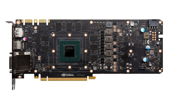
When Apple released the trash can shaped and highly customized Mac Pro design in 2013 – one, coincidentally enough, they’ll be walking away from for the next iteration – Apple also sealed the fate for end-user video card upgrades on the Macintosh platform. Every Mac now uses a customized, integrated video card of some kind, from the soldered-on MacBook Pro up to the custom format cards of the Mac Pro. This has meant that as the old, Westmere-based Mac Pro towers have aged into retirement, so has the market for Mac video card upgrades.
For NVIDIA, this is a bit of a double-whammy. NVIDIA owns the bulk of the discrete video card market, and at the same time, Apple hasn’t integrated an NVIDIA GPU in some time now; the last NVIDIA-equipped Mac was the 2014 MacBook Pro, which included an NVIDIA Kepler GPU. As a result, NVIDIA has been locked out of the Mac video card market entirely for the last couple of years, and consequently makes NVIDIA’s announcement so surprising.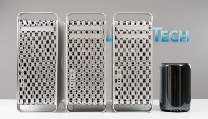
So why is NVIDIA releasing a Mac driver to a market that, officially speaking, is essentially dead? It’s telling that this is a question NVIDIA doesn’t even bother to address, simply stating that they’re “making the new TITAN Xp open to the Mac community with new Pascal drivers” in order to give “Mac users access to the immense horsepower delivered by our award-winning Pascal-powered GPUs.” At best, the official market is the remaining handful of Mac Pro Tower owners.
Instead it’s the off-label use that makes this announcement interesting, and indeed gives NVIDIA any reason whatsoever to make a Pascal driver release. Within the Mac community there are small but none the less vocal user groups based around both unsupported external GPUs and not-even-Apple-hardware Hackintoshes. In the case of the former, while macOS doesn’t support external GPUs (and isn’t certified as eGFX complaint by Intel), it’s possible to use Macs with Thunderbolt eGFX chassis with a bit of OS patching. Meanwhile with a bit more hacking, it’s entirely possible to get macOS running on a custom-built PC, leading to the now long-running Hackintosh space.
The fact of the matter is that neither of these groups is very big relative to the much bigger Mac user base – who wants to do real professional work on an unsupported video card setup? – but they are vocal, and they do need increasingly powerful video cards, like the rest of the PC market. But more to the point, given Apple’s announcement that they’re going to eventually fix the Mac Pro’s GPU woes, but not for at least another year, this is a chance for NVIDIA to take a low-risk pot shot at Apple for their dGPU follies. At a minimum, it’s a nice gesture to Mac users (whom tend to spend big on hardware), and perhaps, it makes for the start of a grassroots campaign to get an NVIDIA GPU in the next iMac or Mac Pro. And while only NVIDIA knows for sure if they planned this before this week’s Mac Pro announcement or they just got lucky, it comes across as a clever move by the company.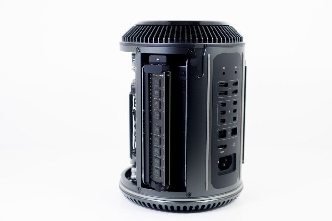
Otherwise, from a technical perspective, there’s little reason for NVIDIA not to do this. The company needs to keep Mac driver development for new architectures alive regardless so that they can compete for future GPU contracts, meaning NVIDIA already has the drivers in-house, though perhaps not in an end-user ready state. Given how the whole endeavor is essentially unsupported from the Appel side of matters, this may make for a bumpy ride at the start. But I think it will be interesting to see where the NV-GPU equipped Mac user base stands in a year or two when Apple readies their next Mac Pro, and if NVIDIA’s gesture has any real impact on the number of NVIDIA users out there.
More...


 Quote
Quote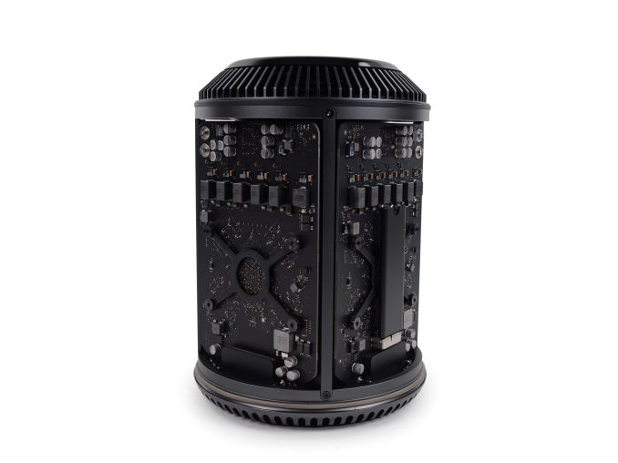
Thread Information
Users Browsing this Thread
There are currently 19 users browsing this thread. (0 members and 19 guests)


Bookmarks