

Results 7,111 to 7,120 of 12096
Thread: Anandtech News
-
06-27-17, 06:13 AM #7111
Anandtech: The Intel SSD 545s (512GB) Review: 64-Layer 3D TLC NAND Hits Retail
64-layer 3D NAND has arrived with Intel as the first to market. The new Intel SSD 545s is a mainstream consumer SATA SSD that greatly improves on last year's disappointing Intel SSD 540s. Intel hasn't quite beaten Samsung's entrenched 850 EVO, but the SSD market is definitely getting more competitive with this new generation of 3D NAND flash memory.
More...
-
06-27-17, 08:00 AM #7112
Anandtech: ASUS & Sapphire Release Pascal & Polaris-based Cryptocurrency Mining Cards
Even during the most bullish Bitcoin days, video card partners had shied away from creating specific SKUs for the purpose of cryptocurrency mining, and that has remained the case since – until now. With the Ethereum mining mania hitting new heights (ed: and arguably new lows), add-in board vendors ASUS and Sapphire have released mining-specific video cards, with variants based off of NVIDIA's GP106 GPU, and AMD's RX 470 & RX 560 video cards. Being built for high hash-rates rather than visual graphics horsepower, these cards are distinctively sparse in their display output offerings.
ASUS has outright labelled their cards as part of their new “MINING Series,” with product pages for MINING-P106-6G and MINING-RX470-4G advertising hash-rate production and cost efficiency features. Something to note is that ASUS has chosen to use the GPU codename of GP106, rather than the NVIDIA GTX 1060 branding. The GP106-based card has no display outputs, while the RX 470 card supports only a single DVI-D output despite humorously having HDMI and DisplayPort cut-outs on the PCIe bracket. Both cards are specified at reference clocks.
Meanwhile, Overclockers UK are listing 5 Sapphire MINING Edition SKUs, with 4 RX 470 variants differentiated by memory manufacturer and VRAM size: RX 470s with 4GB of non-Samsung (11256-35-10G) or Samsung memory (11256-36-10G), RX 470s with 8GB of non-Samsung (11256-37-10G) or Samsung memory (11256-38-10G), as well as an RX 560 Pulse MINING Edition card (11267-11-10G). None of the RX 470 variants offer any display outputs, while the RX 560 has a single DVI-D.

In the Overclockers UK product descriptions, cards with Samsung memory are specified for an additional 1 MH/s (mega-hashes per second) over the non-Samsung counterparts, highlighting the importance of memory bandwidth and quality in current Ethereum mining. In addition, the descriptions state a short 1 year warranty and, interestingly, CrossFire support for up to 2 GPUs. It remains to be seen whether these cards can be paired with standard video cards for the purpose of increased graphical performance.
Other SKU listings have surfaced in the wild: Sapphire RX 470 4GB with non-Samsung (11256-21-21G) and Samsung memory (11256-31-21G) on Newegg, and MSI P106-100 MINER 6G on NCIX. The Newegg Sapphire RX 470s, unlike the ones listed on Overclockers UK, both have single DVI outputs and 180 day limited warranties. However, the MSI mining card is completely bare of any details.
Looking back, Bitcoin, Litecoin, and Dogecoin – as well as many others – have all waxed and waned. Yet video card manufacturers remained the last holdouts in the PC component market in offering cryptocurrency-specific SKUs; since then, there have been tailored chassis’, PSUs, and motherboards both new and old. In the past, surging cryptomining demand has resulted in periodic supply issues, with consequences like $900 R9 290X’s. Now, ASUS and Sapphire seem intent on tackling the current Polaris and Pascal shortages from the most direct angle possible: cryptomining cards.
While drastic on some level, it’s representative of the difficult problem faced by both the GPU manufacturers (AMD and NVIDIA) and their video card partners. Mining-inflated demand restricts supply to such an extent that scarcity and artificially high prices infuriate standard consumers looking to purchase video cards. However, overproduction could easily lead into an intractably congested channel after the cryptomining craze has ceased, not to mention potential RMA/warranty headaches or unintentional flooding of the secondary market with used mining cards of variable health.
By offering cryptomining cards with limited warranties, restricted display outputs, and presumably lower manufacturing costs, vendors are hoping to capitalize on mining demand while satisfying standard consumers and avoiding undue damage to their brand or revenue. Given these aggressive and forthright efforts by ASUS and Sapphire, it would not be surprising if other add-in board vendors followed suit with a few mining-specific products of their own.
More...
-
06-27-17, 08:00 AM #7113
Anandtech: Google Fined 2.42B by European Commission for Antitrust Violations
This morning Google has become a new record holder in the European Union; unfortunately however it’s not a good record to hold.
Capping off a multi-year investigation, the European Commission – the EU’s executive body – has ruled that Google has violated the EU’s antitrust laws with the company’s shopping service and how it is promoted. As a consequence of this ruling, the EU is levying a €2,424,495,000 (~$2.73B) fine against Google, along with requiring the company to cease anti-competitive activities in the next 90 days under threat of further fines. This fine is, in turn, now the largest antitrust fine ever levied by the EU, easily surpassing Intel’s €1.06bil fine in 2009.
The EU has been investigating Google for several years now – and indeed hasn’t been the only body to do so over the years – and based on how the investigation was proceeding, it has been expected for some time now that the European Commission would rule against Google. Overall, the Commission bases the size of the fine on the revenue of the offending business – in this case Google’s shopping comparison service – where it can levy a fine at up to 30% of revenue over the offending period of time. So while Google’s fine is quite large, it also represents an equally significant amount of time – over 9 years in the case of Germany and the UK.
From an antitrust standpoint, the crux of the Commission’s argument has been that Google has leveraged their dominance of the search market to unfairly prop up and benefit their search comparison service. Specifically, that in their search results Google listed their own shopping service and its results ahead of competing services, severely harming competitors, who saw traffic drops of up to 92% depending on the specific country in question.
For the time being, Google has 90 days to fix the issue. The Commission isn’t recommending a specific remedy, but they expect Google to pick a reasonable remedy and to explain it to the Commission. Ultimately what regulations are looking for is that Google give competitors “equal treatment” – that is, that competing shopping comparison services receive equal footing in Google’s search results, following the same methods and processes that Google uses to place their own service. Should Google not comply, then the Commission has the option of levying a further fine of 5% of all of Alphabet’s global daily turnover.
Meanwhile Google has the option of appealing the ruling to the courts, and while they’ve yet to make a decision, they’ve already published their own rebuttal to the Commission’s ruling, indicating that an appeal is likely. In their rebuttal, Google has stated that “While some comparison shopping sites naturally want Google to show them more prominently, our data show that people usually prefer links that take them directly to the products they want, not to websites where they have to repeat their searches.” The company has also noted that they do have competition, particularly from companies like eBay and Amazon.
Finally, along with today’s ruling, the European Commission has also noted that they still have other, ongoing cases against Google that they are continuing to investigate. These include issues over the Android operating system – where the Commission is concerned that “Google has stifled choice and innovation in a range of mobile apps and services by pursuing an overall strategy on mobile devices to protect and expand its dominant position in general internet search” – and Google’s AdSense unit, where there are concerns over Google’s policies have reduced choice in the ad market. As a result, even if Google doesn’t appeal today’s fine, their legal wrangling with the EU is not yet over.
More...
-
06-27-17, 09:58 AM #7114
Anandtech: Honor 9 Makes Its Way West: Launching Today in Europe for £380/450
A couple of weeks back at an event in China, Huawei’s Honor sub-brand announced their flagship smartphone for 2017: the Honor 9. Following in the footsteps of the Honor 8 before it, the Honor 9 continues in Honor’s tradition of offering flagship-level smartphones with high-end components at a more mainstream price. At the time of the reveal, the Honor 9 was only being released in China. But now a short few weeks later, Honor is announcing that it is making its way west for its European launch, which kicks off today.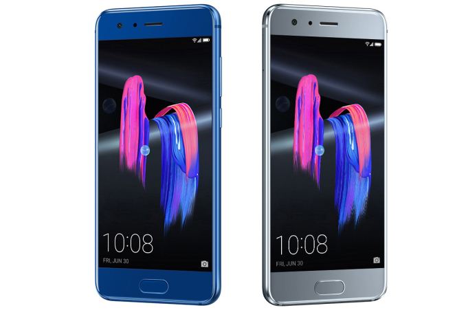
Honor’s latest flagship is a 5.15-inch phone that, at first glance, looks a lot like parent company Huawei’s recently-launched P10 smartphone. The Honor phone gets the same latest-generation Kirin 960 SoC from Huawei’s HiSilicon division, and the 5.15-inch 1080p display is only a hair larger than the P10’s 5.1-inch display. This is similar to what we have seen in past generations, with the Honor flagship serving as a more value-priced alternative for consumers who are after the latest Huawei tech.
Rounding out the specifications, depending on the configuration the phone is paired with either 4GB or 6GB of RAM. All (listed) SKUs come with 64GB of NAND for storage, along with a microSD card for additional storage. For wired connectivity, Honor offers a USB 2.0 port as well as a 3.5mm audio jack. Powering the phone is a 3200mAh battery, which works out to being a bit bigger than the battery on last year’s Honor phone. Finally, Honor has thankfully moved the fingerprint sensor for this year’s phone; rather than being on the rear of the phone it’s now on the front of the phone, where it’s easier to access.Honor Flagship Phones Honor 9 Honor 8 SoC HiSilicon Kirin 960
4x Cortex-A53 @ 1.8GHz
4x Cortex-A73 @ 2.4GHz
ARM Mali-G71 MP8HiSilicon Kirin 950
4x Cortex-A72 @ 2.3GHz
4x Cortex-A53 @ 1.8GHz
Mali-T880MP4 @ 900MHzDisplay 5.15-inch 1920x1080 IPS LCD 5.2-inch 1920x1080 IPS LCD Dimensions 147.3 x 70.9 x 7.45 mm
155 grams145.5 x 71.0 x 7.45 mm
153 gramsRAM 4GB / 6GB 3GB / 4GB NAND 64GB
+ microSD32GB / 64GB (eMMC)
+ microSDBattery 3200 mAh (12.23 Wh)
non-replaceable3000 mAh (11.46 Wh)
non-replaceableModem HiSilicon LTE (Integrated)
2G / 3G / 4G LTE (Category 12/13)HiSilicon Balong (Integrated)
2G / 3G / 4G LTE (Category 6)SIM Size 2x NanoSIM Wireless 802.11a/b/g/n/ac, BT 4.2, NFC, GPS/Glonass/BDS Connectivity USB 2.0 Type-C, 3.5mm headset Launch OS Android 7.1 with EMUI 5.1 Android 6.0 with EMUI 4.1
Meanwhile like the Honor 8 before it, the Honor 9 gets a dual camera implementation. This time however instead of matching color and monochrome cameras, the monochrome camera gets a resolution boost, resulting in a 12MP color (RGB) camera paired with a 20MP monochrome camera. As you’d expect with the significant resolution increase for one of the cameras, along with the more powerful Kirin 960 SoC, the camera is the second major focal point for Honor’s promotion of the phone. Specifically, the company is promising improved low-light photography thanks to the improved monochrome camera.
As for the build of the phone, Honor has once again gone with glass for the front and back of the phone. In fact the overall design of the phone and its construction appears to be very similar to the Honor 8 in this respect; the edge-to-edge glass is comprised of 15 layers, with a 2.5D curve at the edges. New to this year’s model is what Honor is calling “Glacier Grey”, which joins their other color options.
As for the launch of the phone, the Honor 9 is available today in much of Europe, including Germany, Belgium, Italy, Russia, and the UK. Interestingly, different countries are getting slightly different phone configurations: the UK gets a 4GB RAM / 64GB NAND configuration for £379.99, meanwhile the rest of Europe is reportedly getting a 6GB RAM / 64GB NAND configuration for €449.99. As for a US release, Honor isn’t announcing anything at this time. However given Honor’s recent struggles, at this point a US release should not be considered a given.
Gallery: Honor 9 (Blue)


Gallery: Honor 9 Makes Its Way West: Launching Today in Europe for £380/450

More...
-
06-27-17, 11:03 AM #7115
Anandtech: AMDs Radeon Vega Frontier Edition Formally Launches: Air Cooled For $999,
After what appears to be a very unusual false start, AMD has now formally launched their new Radeon Vega Frontier Edition card. First announced back in mid-May, the unusual card, which AMD is all but going out of their way to dissuade their usual consumer base from buying, will be available today for $999. Meanwhile its liquid cooled counterpart, which was also announced at the time, will be available later on in Q3 for $1499.
Interestingly, both of these official prices are some $200-$300 below the prices first listed by SabrePC two weeks ago in the false start. To date AMD hasn’t commented on what happened there, however it’s worth noting that SabrePC is as of press time still listing the cards for their previous prices, with both cards reporting as being in-stock.
[TABLE="align: center"]
[TR="class: tgrey"]
[TD="colspan: 7, align: center"]AMD Workstation Card Specification Comparison[/TD]
[/TR]
[TR="class: tlblue"]
[TD="width: 155"] [/TD]
[TD="width: 120, align: center"]Radeon Vega Frontier Edition[/TD]
[TD="width: 120, align: center"]Radeon Pro Duo (Polaris)[/TD]
[TD="width: 120, align: center"]Radeon Pro WX 7100[/TD]
[TD="width: 120, align: center"]Radeon Fury X[/TD]
[/TR]
[TR]
[TD="class: tlgrey"]Stream Processors[/TD]
[TD="align: center"]4096[/TD]
[TD="align: center"]2 x 2304[/TD]
[TD="align: center"]2304[/TD]
[TD="align: center"]4096[/TD]
[/TR]
[TR]
[TD="class: tlgrey"]Texture Units[/TD]
[TD="align: center"]?[/TD]
[TD="align: center"]2 x 144[/TD]
[TD="align: center"]144[/TD]
[TD="align: center"]256[/TD]
[/TR]
[TR]
[TD="class: tlgrey"]ROPs[/TD]
[TD="align: center"]64[/TD]
[TD="align: center"]2 x 32[/TD]
[TD="align: center"]32[/TD]
[TD="align: center"]64[/TD]
[/TR]
[TR]
[TD="class: tlgrey"]Base/Typical Clock[/TD]
[TD="align: center"]1382MHz[/TD]
[TD="align: center"]N/A[/TD]
[TD="align: center"]N/A[/TD]
[TD="align: center"]N/A[/TD]
[/TR]
[TR]
[TD="class: tlgrey"]Peak/Boost Clock[/TD]
[TD="align: center"]1600MHz[/TD]
[TD="align: center"]1243MHz[/TD]
[TD="align: center"]1243MHz[/TD]
[TD="align: center"]1050MHz[/TD]
[/TR]
[TR]
[TD="class: tlgrey"]Single Precision[/TD]
[TD="align: center"]13.1 TFLOPS[/TD]
[TD="align: center"]11.5 TFLOPS[/TD]
[TD="align: center"]5.7 TFLOPS[/TD]
[TD="align: center"]8.6 TFLOPS[/TD]
[/TR]
[TR]
[TD="class: tlgrey"]Half Precision[/TD]
[TD="align: center"]26.2 TFLOPS[/TD]
[TD="align: center"]11.5 TFLOPS[/TD]
[TD="align: center"]5.7 TFLOPS[/TD]
[TD="align: center"]8.6 TFLOPS[/TD]
[/TR]
[TR]
[TD="class: tlgrey"]Memory Clock[/TD]
[TD="align: center"]1.89Gbps HBM2[/TD]
[TD="align: center"]7Gbps GDDR5[/TD]
[TD="align: center"]7Gbps GDDR5[/TD]
[TD="align: center"]1Gbps HBM[/TD]
[/TR]
[TR]
[TD="class: tlgrey"]Memory Bus Width[/TD]
[TD="align: center"]2048-bit[/TD]
[TD="align: center"]2 x 256-bit[/TD]
[TD="align: center"]256-bit[/TD]
[TD="align: center"]4096-bit[/TD]
[/TR]
[TR]
[TD="class: tlgrey"]Memory Bandwidth[/TD]
[TD="align: center"]483GB/sec[/TD]
[TD="align: center"]2x 224GB/sec[/TD]
[TD="align: center"]224GB/sec[/TD]
[TD="align: center"]512GB/sec[/TD]
[/TR]
[TR]
[TD="class: tlgrey"]VRAM[/TD]
[TD="align: center"]16GB[/TD]
[TD="align: center"]2 x 16GB[/TD]
[TD="align: center"]8GB[/TD]
[TD="align: center"]4GB[/TD]
[/TR]
[TR]
[TD="class: tlgrey"]Typical Board Power[/TD]
[TD="align: center"]
-
06-28-17, 01:32 AM #7116
Anandtech: Qualcomm Announces Snapdragon 450 Midrange SoC
Kicking off today is second Mobile World Congress of the year, MWC Shanghai. As the de facto home of smartphone manufacturing, and home for an increasing number of major mobile device vendors, the tradeshow has taken on increased importance in recent years. This year is no exception, with several different announcements of note coming out of the show.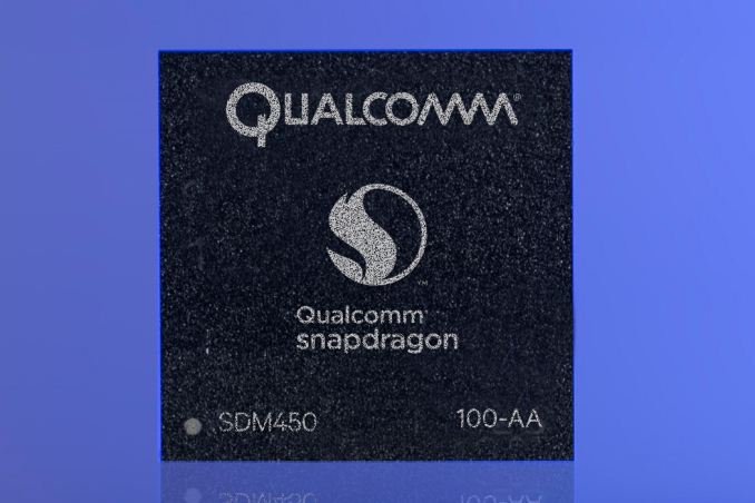
Starting things off for everyone is Qualcomm, who is at the show to announce their latest mainstream Snapdragon 400 series SoC: the Snapdragon 450. The successor to Qualcomm’s 2016 Snapdragon 435, the Snapdragon 450’s biggest claim to fame is also its smallest: it will be the first Snapdragon 400 series SoC to be fabbed at 14nm, finally moving Qualcomm’s mainstream SoC lineup off of 28nm LP and on to a more recent and more power efficient manufacturing node.
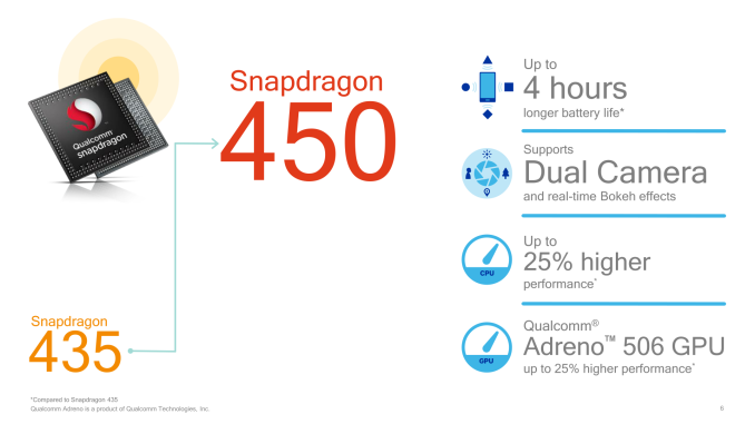 At a high level, the Snapdragon 450 is a very straightforward successor to the 435. Qualcomm has taken most of the 435’s design principles and brought them forward for the smaller Snapdragon 450. For example, we’re still looking at an octa-core ARM Cortex-A53 implementation, however thanks to the 14nm process Qualcomm has been able to bump up the maximum clockspeed from 1.4GHz to 1.8GHz. Similarly, Qualcomm has updated the GPU from an Adreno 505 on the Snapdragon 435 to an Adreno 506 on the Snapdragon 450, with the more powerful GPU said to offer 25% better performance.
Qualcomm Midrange Snadpragon Family SoC Snapdragon 450 Snapdragon 435 Snapdragon 625 CPU 4x A53 @ 1.8GHz
4x A53 @ 1.8GHz4x A53 @ 1.4GHz
4x A53 @ 1.4GHz4x A53 @ 2.0GHz
4x A53 @ ? GHzMemory 1x 32-bit LPDDR3 1x 32-bit @ 800MHz
LPDDR3
6.4GB/s b/w1x 32-bit @ 933MHz
LPDDR3
7.45GB/s b/wGPU Adreno 506 Adreno 505 Adreno 506 Encode/
Decode1080p
H.264 & HEVC (Decode)1080p
H.264 & HEVC (Decode)2160p
H.264 & HEVC (Decode)Camera/ISP Dual ISP
13MP + 13 MP (Dual)
21MP (Single)Dual ISP
8MP + 8MP (Dual)
21MP (Single)Dual ISP
24MPIntegrated
Modem"X9 LTE" Cat. 7
300Mbps DL 150Mbps UL
2x20MHz C.A.
(DL & UL)"X9 LTE" Cat. 7
300Mbps DL 100Mbps UL
2x20MHz C.A.
(DL & UL)"X9 LTE" Cat. 7
300Mbps DL 150Mbps UL
2x20MHz C.A.
(DL & UL)USB 3.0
w/QuickCharge 3.02.0
w/QuickCharge 3.03.0
w/QuickCharge 3.0Mfc. Process 14nm 28nm LP 14nm
Meanwhile more significant upgrades have been made to the ISPs and USB controller. Similar to the Snapdragon 435, the 450 supports a single camera at up to 21MP. However if it’s used in a dual camera configuration – as is increasingly popular these days for artificial Bokeh and telephoto modes – then it can handle a pair of 13MP sensors, up from 8MP on the Snapdragon 435, and a notable improvement as 13MP seems to increasingly be the baseline for midrange phones. Qualcomm’s video processor blocks have also been improved, in part to keep up with the improved sensor, and as a result the 450 can now capture video at up to 1080p60, doubling the maximum framerate over the Snapdragon 435’s 1080p30 limit. Meanwhile the USB controller has been upgraded from USB 2.0 to USB 3.0, allowing for much faster transfers from Snapdragon 450 devices. And, like its predecessor, the 450 also supports QualComm’s QuickCharge 3.0 tech over said USB port.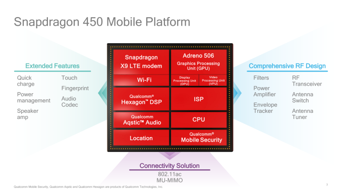
Cellular connectivity is once again provided by Qualcomm’s Integrated X9 modem, which supports LTE Category 7 down and Category 13 up, for a maximum of 300Mbps down and 150Mbps up respectively. Interestingly, on the Snapdragon 435, Qualcomm limited that SoC for just 100Mbps up despite the fact that Category 13 allows for 150Mbps; so this is the first X9-equipped Snapdragon 400 SoC to actually be able to hit 150Mbps up, going by Qualcomm’s specifications. The 450 also retains the 435’s Hexagon DSP, however like so many other parts of the SoC, the 450’s DSP has been further enhanced to reduce power consumption.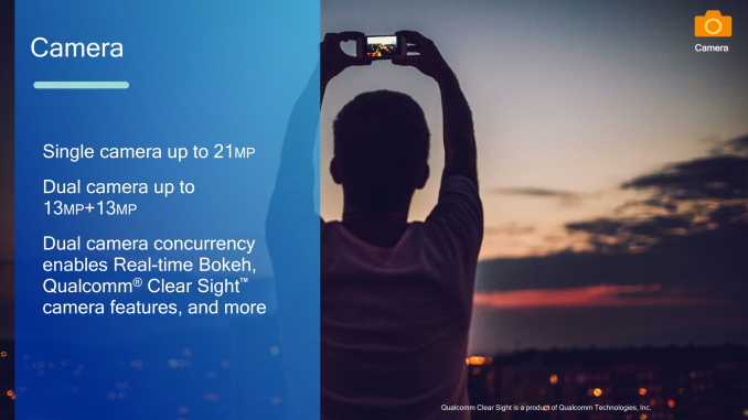
Last but not least, Qualcomm is promising some solid battery life improvements with the Snapdragon 450 over its 435 predecessor. While the company has invested some of their 14nm gains in improving clockspeeds throughout the chip, they’ve also retained a lot of those gains for reducing overall power consumption, a philosophy similar to what they did with the Snapdragon 835 this year as well. To that end the company is promoting that Snapdragon 450 phones will be able to deliver 4 hours more battery life relative to 435 phones.
Overall it’s interesting to note just how much the Snapdragon 450 sounds a lot like Qualcomm’s Snapdragon 625, their 14nm SoC from 2016. Both chips use a octa-A53 CPU configuration, X9 LTE modem, and Adreno 506 GPU. In fact the Snapdragon 450 is even pin compatible with the Snapdragon 625, which means that handset manufacturers can immediately begin working with the new SoC in existing designs. However given this close similarity, I’m also left to wonder whether the Snapdragon 450 is a new die, or a cut-down 625. In any case, the two chips still have some differences between them: particularly that the Snapdragon 625 clocks higher and features a more powerful ISP and video decode block.
Wrapping things up, as is often the case with Qualcomm’s SoC reveals, today’s announcement comes ahead of vendor sampling and wide release. The company will begin commercial sampling in Q3 of this year, and the chip should show up in retail devices by the end of the year.
Gallery: Qualcomm Snapdragon 450 Press Deck


More...
-
06-28-17, 06:41 AM #7117
Anandtech: Qualcomm Announces Snapdragon Wear 1200 SoC: LTE Categories M1 & NB1 for W
Back around this time last year, Qualcomm introduced their Snapdragon Wear 1100, the company’s first SoC specifically designed for budget, low-power wearable devices. The humble SoC featured just a single Cortex-A7 CPU core and LTE Cat 1 support, but for the market Qualcomm had designed it for, this was more than sufficient. Now at MWC Shanghai 2017, the company is launching an even more low power successor to the Snapdragon Wear 1100, the aptly named Snapdragon Wear 1200.
The Snapdragon Wear 1200 is an interesting development from Qualcomm, as while the name can be a bit deceiving, it’s the first in a new generation of products for the company. Taking the basic principles of the 1100, Qualcomm has integrated a new modem that supports new, ultra-low-power communication modes for LTE standardized in the last year: LTE Category M1 and Category NB1. In fact this is Qualcomm’s first SoC to support the 3GPP’s Low Power WAN technologies.
Briefly touching on the specs of the Wear 1200, the core processor is almost unchanged from the Wear 1100. The SoC is still powered by a single Cortex-A7 CPU core and paired with a simple display controller that is just barely a fixed function GPU. It is meant to be a low-power (and low cost) SoC, through and through.Qualcomm Snapdragon Wear SoCs Snapdragon Wear 1200 Snapdragon Wear 1100 Snapdragon Wear 2100 SoC Cortex-A7 @ 1.3GHz
Fixed-function GPUCortex-A7 @ 1.2GHz
Fixed-function GPU4x Cortex-A7 @ 1.2GHz
Adreno 304Process Node 28nm LP 28nm LP 28nm LP RAM LPDDR2 LPDDR2 LPDDR3-800 MT/s Display Simple 2D UI Simple 2D UI Up to 640x480 @ 60fps Modem Qualcomm (Integrated)
2G (E-GPRS) / LTE
(Cat M1 & Cat NB1)Qualcomm (Integrated)
2G / 3G / LTE (Category 1 10/5 Mbps)Qualcomm X5 (Integrated)
2G / 3G / LTE (Category 4 150/50 Mbps)
Connected version onlyConnectivity 802.11b/g/n/ac, BT 4.2 LE, GPS/GLONASS/Galileo/BeiDou 802.11b/g/n/ac, BT 4.1 LE, GPS/GLONASS/Galileo/BeiDou
(Wi-Fi and BT optional)802.11b/g/n (2.4GHz),
BT 4.1 LE, NFC, GPS/GLONASS/Galileo/BeiDou, USB 2.0
Connected and Tethered versions
The big change here for Qualcomm is on the modem side. Whereas the Wear 1100 shipped with a multi-mode 2G /3G / LTE Cat 1 modem – as low a power a design as one could get at the time – the Wear 1200 incorporates a much more power-efficient and very much forward-looking modem. One that supports only basic 2G (E-GPRS) functionality, along with the aforementioned LTE Cat M1 and NB1 standards.
This is the first product announcement to cross our desk supporting these new standards, and ultimately the Snapdragon Wear 1200 will be the first of many devices/chips that we see to do so. Part of the 3GPP’s Release 13, the standards body has been focusing on reducing power consumption, complexity, and costs for radios for IoT devices, wearables, and other simple devices as part of their LPWAN initiative.
At a high level, LTE Cat M1 is designed to be a relatively straightforward, further power-optimized form of LTE. The max data rate is just 1Mbps up and down – and the Wear 1200 doesn’t even reach those speeds – using tricks like a minimum-width 1.08Mhz channel and half-duplex communication to cut power consumption, all the while still being compatible with existing LTE networks. LTE Cat NB1 takes this a step further, going with a stand-alone LTE-derived narrowband implementation that uses just a 180KHz channel, which combined with other technologies offers the lowest amount of bandwidth (max 250Kbps) but also the lowest power consumption and improved range.
For Qualcomm and other wearable/IoT device manufacturers, these new standards will be a significant part of making the Internet of Things live up to its name, by allowing even the lowest-power, lowest-cost devices to have LTE network functionality. Unsurprisingly then, one of the first places we’re going to see it deployed is in low-cost wearables, where Internet access is beneficial, but battery life concerns are significant.3GPP Low Power WAN LTE Standards LTE Cat M1 LTE Cat NB1 Network Type LTE-Compatible Seperate Band Bandwidth 1.08MHz 180KHz Peak Download 1 Mbps 250 Kbps Peak Upload 1 Mbps 250 Kbps / 20 Kbps
As for the Wear 1200 in particular, Qualcomm’s wearable-class SoC keeps a low profile even for M1/NB1 devices. The SoC can support 300Kbps down and 375Kbps up for Cat M1, and just 20Kbps down and 60Kbps up for Cat NB1. And no, the latter isn’t a typo: NB1 devices are expected to send data as much (if not more than) they receive it, so the Wear 1200’s data rates vary accordingly. Meanwhile, despite the limited bandwidth these standards offer, the Wear 1200 supports 15 RF bands along with some notable LTE features, particularly VoLTE. Interestingly however, while Qualcomm supports the latest low-power IoT standards, they don’t support the equivalent low-power 2G standard, EC-GSM. The Wear 1200 does support 2G in the form of E-GPRS, so there is GSM backwards compatibility for when LTE isn’t available, but the future Qualcomm is planning for is very much one where LTE is everywhere and 2G won’t be needed.
Modems aside, the Wear 1200 is otherwise a function-optimized design. Like its predecessor, the SoC supports WiFi and Bluetooth for various connectivity options, along with augmenting the standard GPS/GLONASS/Beidou/Galileo geo positioning systems. The new SoC retains the same small size of its predecessor, with the chip measuring 79mm2. Overall, Qualcomm is touting a 10 day standby battery life for the SoC, which would be a significant improvement over the 7 day standby of the Wear 1100.
Finally, looking at the broader picture, the wearables market is still trying to figure out what it wants to be – and what consumers will actually buy – and for the Wear 1200 Qualcomm is particularly interested in courting the “kid watch” market. A segment of the larger smart tracker market, Qualcomm is looking to tap into what is already a significant market in Asia – and especially China – where it’s not uncommon to give your kid a limited functionality watch that allows you to contact them, while the watch works in conjunction with geofencing applications to keep tabs on their whereabouts. Driven in part by demographics and in part by technology, Qualcomm expects the market for kid tracking watches to further grow, with SoCs like the Wear 1200 further improving the utility of these devices and bringing their cost down. These improvements would also filter down to other parts of the smart tracker market, such as pet tracking and elderly tracking devices.
In fact the company is hitting the ground running: along with the launch of today’s SoC, they are also partnering with Borqs and Quanta to develop smart tracker/kid watch reference designs, so that hardware manufacturers can get a jump on developing Wear 1200-based trackers. And like the Snapdragon Wear 1200 itself, these reference designs are available and shipping today. So while Qualcomm isn’t specifically commenting on when their customers’ consumer devices will be ready, it will almost certainly be before the end of the year.
More...
-
06-28-17, 08:26 AM #7118
Anandtech: Western Digital My Passport SSD Mini-Review
Flash-based external direct-attached storage (DAS) devices have evolved rapidly over the last few years. Starting with simple thumb drives that could barely saturate USB 2.0 bandwidth, we now see high-performance external SSDs. The full performance from these new crop of external storage devices can only be realized using the USB 3.1 Gen 2 interface. Western Digital's My Passport SSD is an external SSD with a USB 3.1 Gen 2 Type-C interface. It caters to the mainstream market and comes in three capacities - 256GB, 512GB, and 1TB.In this review, we take a look at the 1TB version.
More...
-
06-28-17, 09:15 AM #7119
Anandtech: Western Digital Announce BiCS4 3D NAND: 96 Layers, TLC & QLC, Up to 1 Tb p
Western Digital on Tuesday formally announced its fourth-generation 3D NAND memory, developed as part of the Western Digital/Toshiba joint venture. The fourth-generation BiCS NAND flash chips from Western Digital feature 96 layers and will include several capacity points and will use TLC and QLC architectures. The company expects to start volume production of BiCS4 chips in 2018.
NAND dies that belong to the fourth-generation BiCS 3D NAND will use 96 word layers to minimize die size of the chips and maximize output of fabs, and at this point represents the largest layer count in the flash memory industry. Furthermore the range of BiCS4 NAND die configurations available will be considerably more diverse than BiCS3, which currently only includes 256 Gb and 512 Gb dies. Western Digital plans to offer BiCS4 components based on TLC (triple level cell) and QLC (quadruple level cell) configurations. with capacities ranging from 256 Gb to 1 Tb.
It is noteworthy that Western Digital’s BiCS4 lineup will include QLC NAND, which has been discussed by Western Digital (and SanDisk before that) for several years, but which is about to become reality only in the coming quarters. To store four bits per cell (with 16 voltage states) Western Digital had to use a “thick” process technology alongside multi-layer 3D NAND to keep the per-bit costs down. The company is not specifying how many program/erase cycles its 3D QLC NAND will handle, but various industry predictions over the years have suggested 100 – 150 P/E cycles as a reasonable goal for QLC NAND, which is considerably lower than approximately 1000 P/E cycles supported by TLC NAND. Given such endurance, it is logical to expect 3D QLC NAND to be used for primarily removable storage as well as for ultra-high capacity datacenter drives for the so-called near-WORM (write once read many) storage applications. For example, Toshiba last year discussed a QLC-based datacenter SSD with 100 TB capacity for WORM apps.
Western Digital plans to begin sampling of select 96-layer BiCS4 3D NAND configurations in the second half of this year, but the manufacturer does not specify which dies will sample when. As for mass production, Western Digital intends to start volume manufacturing of their 96-layer 256 Gb 3D NAND in 2018, with other dies to follow later. Based on Western Digital’s announcements made earlier, the company will gradually introduce more sophisticated BiCS4 96-layer configurations in 2018 and 2019, before moving to BiCS5 sometimes in 2020. That said, it makes sense to expect the highest capacity BiCS4 ICs to ship later rather than sooner.
Finally, Western Digital did not disclose whether it uses NAND string stacking technology to assemble its 96-layer 3D NAND dies, but it is a likely scenario given what industrial publications have been predicting.
Related Reading:
- WD Blue 3D NAND SATA & SanDisk Ultra 3D SSDs Launched: 3D TLC NAND, SATA, Marvell
- Western Digital Ships Client SSDs Based on 512 Gb 3D TLC NAND Chips
- Toshiba Samples 64-Layer 512 Gb BiCS 3D NAND, Announces 1 TB BGA SSD
- Toshiba Finalizes Plans for New 3D NAND Fab: Coming Online in 2019
More...
-
06-28-17, 08:14 PM #7120
Anandtech: Micron Discontinues Lexar Business, Plans to Focus on Higher-Margin Produc
Micron this week announced plans to discontinue its Lexar removable media storage business as a part of the company’s strategy to shift to higher margin NAND flash-based products. The company intends to sell all or part of its Lexar business division, but promises to support existing customers during the transition period.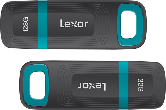
Lexar was spun off from Cirrus Logic in 1996 and then acquired by Micron in 2006 in a bid to market NAND flash media. Approximately two years ago, Micron cut down supply of NAND memory to spot market in a bid to concentrate on building its own products and thus earn higher profit margins. Last year the company announced plans to work with its clients to build software for their software storage offerings to improve its profit margins further this time from various SSDs. In addition, the company disclosed plans to develop special memory solutions for emerging automotive applications (which will complement its embedded portfolio). This week Micron went even further and disclosed plans to cease selling Lexar branded products to consumers and OEMs as a part of its strategy to increase “opportunities in higher value markets and channels.” The portfolio of Lexar products includes memory cards and card readers, USB flash drives and even SSDs.
Given the competition on the market of retail removable media and storage drives, the withdrawal from such businesses may be logical for Micron, which feels increasing pressure from Samsung, Western Digital (SanDisk) and others amid lack of market growth in terms of NAND bits (at least, according to its own predictions). Meanwhile, the withdrawal also means that Micron will have to concentrate on production of SSD-graded memory, whereas NAND for removable storage will be sold on the open market, in case the company continues to develop it. If someone buys the Lexar operations from Micron, the latter will likely sign some kind of exclusive supply agreement with the new owner, which means that it will keep developing the aforementioned NAND. SSD-graded memory is more expensive than chips for memory cards or USB flash drives and for about a year Micron was the only company to sell its SSD-graded 3D NAND to third-party makers of drives, possibly earning higher margin than by selling removable storage devices. However, NAND for the latter is typically used to test drive new production technologies and/or architectures before deploying them to make memory for SSDs.
Micron will not be the only producer of NAND flash, which does not produce its own memory cards and USB flash drives. SK Hynix and Intel also do not produce such products under their own trademarks, unlike Samsung, Toshiba and Western Digital. That said, while it will be sad to see Micron’s Lexar gone (assuming that nobody buys it), Micron’s withdrawal from removable storage business is not exactly surprising.
Related Reading:
- Micron Hires New CEO: Sanjay Mehrotra, SanDisk Co-Founder And Former CEO
- Lexar Launches 'JumpDrive Tough' USB Drives up to 128GB: Focusing on Physical Endurance
- Micron Presents New SSDs and Strategy: From Components to Whole Solutions, 3D NAND Shipping Imminent
- Lexar Professional Workflow HR2 4-Bay Thunderbolt 2 / USB 3.0 Reader Hub Review
More...


 Quote
QuoteThread Information
Users Browsing this Thread
There are currently 40 users browsing this thread. (0 members and 40 guests)


Bookmarks